第四章电子衍射3_11-10-12讲义
- 格式:pdf
- 大小:599.77 KB
- 文档页数:5
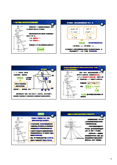

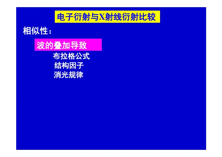
电子衍射与X射线衍射比较相似性:波的叠加导致布拉格公式结构因子消光规律s s v v vK称为电子衍射相机常数λ0S v λS vg hkl vλ0S v λS vg hkl v衍射斑点矢量是产生这一斑点晶面组的倒易矢量的比例放大,K是放大倍数故仅就衍射花样的几何性质而言:单晶花样中的斑点可以直接看成是相应衍射晶面的倒易阵点,各个斑点的就是相应的,之间的夹角就等于产生衍射的两个晶面之间的夹角。
g v R v R v g v R vfr多晶电子衍射花样的标定及其应用二、应用1、已知晶体标定仪器的相机常数KRd =150kv加速电压下拍得多晶金的衍射花样①测量环的半径R i从里向外测得圆的直径:2R 1=17.6mm 、2R 2=20.5mm 、2R 3=28.5mm ,………即R l =8.8mm ,R 2=10.3mm 、R 3=14.3mm 、……已知金为面心结构,a =0.407nm②计算R i 2及R i 2/R 12(R 1—最小半径),根据R i 2/R 12确定衍射环指数8:4:3R :R :R 232221=18:6:4:2 17.9:00.3:98.1:1R :R :R :R 2D2C 2B 2A ==简单立方:1,2,3,4,…体心立方:2,4,6,8,10,12,…h+k+l=2n 面心立方:3,4,8,11,12,16,19,20,…全奇全偶满足体心结构标准花样对照法:由R=Kg可推知:单晶电子衍射花样实质是满足衍射条件的某个零层倒易面的放大像。
∗0]uvw [对于本例,可知,衍射花样是的放大像∗0]110[单晶电子衍射花样分析三、应用1、物相鉴定原理与X射线相同,根据d值和强度查PDF卡片但仅跟据某一晶带的衍射斑点,d值不够8个。
须倾动晶体样品,拍摄不同晶带的衍射花样。
根据化学成分,热处理工艺,可将待测相限制为几种可能,可根据下面三个条件,仅由一张花样鉴别。
<1>点阵类型与PDF卡片相符<2> 衍射斑点必须自洽<3> 底指数晶面间距与卡片的标准相符,允许误差3%左右单晶电子衍射花样分析三、应用2、晶体取向关系的验证和确定<1> 两相取向关系常用两相的一对互相平行的晶面及面上平行的晶向来表示()()[]BA BA w v u //]uvw [l k h //hkl ′′′′′′()()()()()()B 333A 333B 222A 222B 111A 111l k h //l k h l k h //l k h l k h //l k h ′′′′′′′′′表示:面或三对平行的晶向来有时也用三对平行的晶[][][]333A 333B 222A 222B111A 111w v u //]w v u [w v u //]w v u [w v u //]w v u [′′′′′′′′′)),根据()110()011()020()111()111()200(200()202B(h 2k 2l 2)C E F A(h 1k 1l 1)1g v 2g v 'g v D O gv 乘一个系数n,使(hkkl)转化为整数爱瓦尔德球像L 1电子衍射中间镜的物平面与背焦面物镜一次像中间镜投影镜二次像终像。
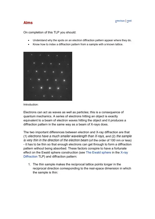
Aims previous | next On completion of this TLP you should:∙Understand why the spots on an electron diffraction pattern appear where they do.∙Know how to index a diffraction pattern from a sample with a known lattice.Introduction:Electrons can act as waves as well as particles; this is a consequence of quantum mechanics. A series of electrons hitting an object is exactly equivalent to a beam of electron waves hitting the object and it produces a diffraction pattern in the same way as a beam of X-rays does.The two important differences between electron and X-ray diffraction are that (1) electrons have a much smaller wavelength than X-rays, and (2) the sample is very thin in the direction of the electron beam (of the order of 100 nm or less) - it has to be thin so that enough electrons can get through to form a diffraction pattern without being absorbed. These factors conspire to have a fortunate effect on the Ewald sphere construction (see The Ewald sphere in the X-ray Diffraction TLP) and diffraction pattern:1. The thin sample makes the reciprocal lattice points longer in thereciprocal direction corresponding to the real-space dimension in which the sample is thin:It should be noted that there is not necessarily always a particular plane oriented like this. However, it is usual for identification of crystallinephases in a sample to orient the sample so that the electron beam isparallel to a low index lattice direction, as this makes the electrondiffraction pattern easier to interpret.2. The small electron wavelength makes the radius of the Ewald spherevery large (recall its radius is 1/λ). The small electron wavelength alsomakes the diffraction angles θ small (1-2°); this can be seen bysubstituting a wavelength of 2.51 x 10⁻¹² m into the Bragg equation (see The Bragg law in the X-ray Diffraction TLP).These make the Ewald sphere diagram look like this so that whole layers of the reciprocal lattice end up projected onto the film or screen:Note that the large (strong) spot in the middle is the straight-through beam (the beam which has passed through the sample without diffracting). This always has the index 000.Caution 1: systematic (kinetic) absences appear in electron diffraction patterns just as in X-ray diffraction patterns, for the same reason: the various features of the lattice or motif diffract electrons in the same direction but the phase factors from the various features cancel, leaving an absence.Caution 2: sometimes where there should be a systematic absence, the spot appears to be still there. This is because of the strong interaction between electrons and atoms: there is a small but significant probability that an electron will be diffracted twice, from two planes one after another - i.e. in two different reciprocal lattice directions one after another. These two directions can add up so that the twice-diffracted electron may arrive at a position in reciprocal space where there is a systematic absence. As an example, the diagram below is a schematic of the [011] electron diffraction pattern of silicon: the 200 type reflections are systematically absent. The intensity at the 200 reflections is caused by double diffraction (arising from the addition of the two reciprocal lattice vectors shown). Thus, in words, intensity can occur in the 200 reflectionfrom, firstly, diffraction from the 11planes, followed by, secondly, difraction by the 1 1 planes as the electron wave passes throught the specimen.Mathematics relating the real space to the electron diffraction patternThe distance, r hkl , on the pattern between the spot hkl and the spot 000 is related to the interplanar spacing between the hkl planes of atoms, d hkl , bythe following equation:(Derivation )where L is the distance between the sample and the film/screen.We can therefore say that the diffraction pattern is a projection of thereciprocal lattice with projection factor L , because reciprocal lattice vectors have length 1/d hkl .Relation 2Since the diffraction pattern is a projection of the reciprocal lattice, the angle between the lines joining spots h 1k 1l 1 and h 2k 2l 2 to spot 000 is the same as the angle between the reciprocal lattice vectors [h 1k 1l 1]* and [h 2k 2l 2]*. This is also equal to the angle between the (h 1k 1l 1) and (h 2k 2l 2) planes, orequivalently the angle between the normals to the (h 1k 1l 1) and (h 2k 2l 2)planes. This angle is θin the diagram below.Using these two relations between the diffraction pattern and the reciprocal lattice, we are now able to index the electron diffraction pattern from a specimen of a known crystal structure.The two pages linked to here refer only to indexing the central region of the diffraction pattern - the rest will be dealt with later.back Indexing with the orientation of the electron beamknownFrom the Ewald sphere diagram, we know that the zero order Laue zone (ZOLZ) contains reflections hkl where hu + kv + lw= 0 (the Weiss zone law). This ZOLZ can be identified by finding two reciprocal lattice vectors in theZOLZ. Suppose these two reciprocal lattice vectors are h1a* + k1b* + l1c* and h2a* + k2b* + l2c*. Then we knowh1u + k1v + l1w= 0andh2u + k2v + l2w= 0and that the angle between these reciprocal lattice vectors is the angle between the h1k1l1 and h2k2l2 planes.Other reflections in the electron diffraction pattern can then be deduced from simple vector addition, with the proviso that the indices of the reciprocal lattice vectors are integers and that they are not forbidden by the lattice. The pattern can then be built up manually or by computer.Example of indexing with a known electron beam orientationbackSuppose the material under examination is copper, and suppose the electron beam direction is [211]. Copper has a cubic close packed structure with a lattice parameter, a, of 0.361 nm. Allowed reflections must have h,k,l either all even or all odd. Thus the planes with the highest interplanar spacings (and hence those that give rise to reflections with the smallest r hkl values) are {111}, {200}, {220}, {311}, {222}, etc.Looking at the {111} planes, it is apparent that the Weiss zone law is obeyedfor (11) when [uvw] =[211]. Hence 11 is a possible reciprocal latticevector.No {200} plane will obey the Weiss zone law for [uvw] = [211], but of the{220} planes it is apparent that (02) will. Hence 02is a second possible reciprocal lattice vector.The angle between the 11 and 02reciprocal lattice vectors is 90° - the dot product of these two reciprocal lattice vectors is zero. The ratio of thelengths of these two reciprocal lattice vectors is . These are the two shortest reciprocal lattice vectors in the [211] electron diffraction pattern. Thus the pattern looks like:back Indexing with the orientation of the electron beamunknownIf we do not know the beam orientation, it is rather more difficult to find which reciprocal plane is the one projected down onto the film.One approach is to consult tables of angles and distance ratios for the low index reflections for the structure of the crystal we are imaging. Again, we will use copper as an example.Table of anglesThe angles in this table are the angles between the reciprocal lattice vectors given at the sides of the table in the appropriate row and column. Such aTable of distance ratiosThe dimensionless numbers in the central portion are the ratios of the 1/d hklexcluded. Thus for copper, which has an F lattice, the reflections are those with h ,k ,l all even or all odd.Now we pick two spots on the diffraction pattern and measure the angle between them and the ratio of their distances from the 000 spot - and see if they correspond to any of the values in the tables.View an exampleOnce we know for sure what two of the non-collinear dots are, we can index the rest of the pattern by vector addition.Example of indexing with an unknown electron beamorientationbackIf were 72.5° and we were to measure the ratio x/y and find it to benumerically equal to 1.66 then we could be reasonably convinced that the dot at Y could be labelled as the 200 spot, and the dot at X could be labelled as 113. In this case our predicted electron beam direction is in thedirection common to the 200 and 113 planes, i.e. [03]. This particular electron diffraction pattern has a central rectangular repeat. If this is correct, further spots on this diffraction pattern can be indexed in aself-consistent manner by vector addition.Laue zoneSo far we have been looking at the central region of the diffraction pattern. This is only a part of the total diffraction pattern. If we look again at the Ewald sphere construction, we have:We have been indexing the portion in the middle with the 000 spot in it. However, there are also areas of diffraction spots at the edges of the film, caused by the Ewald sphere intersecting points in an adjacent parallel plane containing reciprocal lattice points. (If the film was small or the camera length large it is possible that it did not catch these spots at the side, so that we sometimes only have the middle part.)These outlying parts of the diffraction pattern are called Higher Order Laue Zones (HOLZs). Each of the HOLZs can be described by an equation of the general formhu + kv + hw Nwhere:∙N is always an integer, and is called the order of the Laue zone.∙[uvw] is the direction of the incident electron beam.∙hkl are the co-ordinates of an allowed reflection in the N th order Laue zone.The middle part of the diffraction pattern, with 000 in it, is the zero order Laue zone (ZOLZ), because it comes from the plane for which N =0: an allowed reflection hkl in the ZOLZ is joined to the origin 000 by a reciprocal lattice vector that lies in the ZOLZ. For the ZOLZ the electron beam [uvw] and the allowed reflection hkl satisfy the Weiss zone law hu + kv + lw= 0. The next layer up has a value N =1, then N =2, and so on, as shown.From the geometry of the way in which the Ewald sphere intersects the HOLZs, the radius of the N th HOLZ ring, R n, in reciprocal space, is given to a very good approximation by the formulaassuming that the wavelength of the electrons is much less than the modulus |uvw| of the direction [uvw] in the crystal parallel to the electron beam direction. Thus, HOLZs are seen more easily at lower voltages (e.g. 100 kV rather than 300 kV) and when the electron beam is parallel to a relatively high index direction in a crystal.It is possible to index the reflections in the HOLZs on a diffraction pattern. Examples of such indexing are given in the book Transmission Electron Microscopy of Materials by D B Williams and C B Carter.Kikuchi lines previous | next Kikuchi lines often appear on electron diffraction patterns:An example of a "two-beam" electron diffraction pattern with a number of Kikuchi lines.A pair of Kikuchi lines is arrowed.[The term "two-beam" denotes the fact that the straight-through beam, 000, and one diffraction spot are both diffracting very strongly. The intensity of all spots in this electron diffraction pattern are significantly weaker by comparison with these two beams.](Click on image to view larger version)We will not learn to index the Kikuchi lines in this TLP. Instead, we will explain their origin and behaviour with the help of the following animation.Kikuchi lines are interesting because of what they do when the crystal is moved in the beam. Diffraction spots fade or become brighter when the crystal is rotated or tilted, but stay in the same places; the Kikuchi lines move across the screen.The difference in behaviour can be explained by the position of the effective source of the electrons that are Bragg-scattered to produce the two phenomena. The diffraction spots are produced directly from the electron beam, which either hits or misses the Bragg angle for each plane; so the spot is either present or absent depending on the orientation of the crystal. The source of the electrons that are Bragg-scattered to give Kikuchi lines is the set of inelastic scattering sites within the crystal. When the crystal is tilted the effective source of these inelastically scattered electrons is moved, but there are always still some electrons hitting a plane at the Bragg angle - they merely emerge at an angle different to the one that they did before the crystal was tilted.Using polycrystalline materials in the TEM previous | next Just as with X-rays, a completely isotropic fine-grained polycrystalline sample will give a diffraction pattern of concentric rings in the zero order Laue zone (ZOLZ), as the many small crystals at random orientations produce a continuous angular distribution of hkl spots at distance 1/d hkl from the 000 spot - a ring of radius 1/d hkl around the 000 spot for each allowed reflection. The rings are then indexed according to the order of allowed reflections within the ZOLZ.As the grain size increases, the rings within the diffraction pattern break up into discontinuous rings containing discrete reflections. If there is any texture (preferred orientation) within the specimen, arcs may be seen instead of complete rings.Convergent beam electron diffraction (CBED)previous | next When a convergent beam is used instead of a parallel beam of electrons, the rays converge to a point within the specimen and come out the other side inverted like a camera. However, we do not look at the inverted image; we look at the diffraction pattern, with the spots magnified:Depending on the camera length chosen, either the zero order Laue zone can be examined or the zero order Laue zone and higher order Laue zones. Two examples of CBED images are shown below. The symmetry seen is such patterns can be related to the space group symmetry of the specimen.Examples of CBED images:Diffraction pattern showing a zero order Laue zone with a mirror in the pattern as shown(Click on image to view larger version)Diffraction pattern showing a first order Lauezone(Click on image to view larger version)Using other methods in conjunction with electrondiffraction previous | next Electron diffraction is a powerful technique - but other techniques must be used with it to put the results in context. This is a brief synopsis of how other methods can be used to help.Optical imagingThis is a very important way of analysing a specimen. Using the naked eye and optical microscopes we can determine down to a point-to-point resolution limited by the wavelength of light how many phases there are and how they relate to one another. We can also infer what type of material they are likely to be and how they may have been processed.Chemical analysisA wide range of chemical techniques can be used to find out what components are present in the different phases and in what proportions. This will narrow the field of possible elements that we need to consider when analysing ourdiffraction results. These techniques range from simple chemical tests, through infrared spectroscopy of organic samples, to a wide variety of chemical characterisation techniques that can often be performed within thetransmission electron microscope.TEM imagingUsing the TEM to image the same area of sample that is being used toproduce the diffraction pattern is an invaluable technique:Nitrided surface layer of austenitic stainlesssteel(Click on image to view larger version)Diffraction pattern from nitrided surface layer of austenitic stainless steel (Click on image to view larger version) Using the image to verify that the double dots in the diffraction pattern arebeing caused by the two crystal structures either side of the twin boundary, we can index the pattern and determine the twin plane and the crystal structures either side of it.Summary previous | next In this teaching and learning package we have considered how electron diffraction patterns are formed in the transmission electron microscope. The principles of how to index spot electron diffraction patterns have been discussed in some detail. Although we have considered how to index electron diffraction patterns from relatively simple crystal structures toillustrate the basic principles, these principles are generic and can therefore be applied to any crystal structure. We have also considered other features of electron diffraction patterns such as the formation of Kikuchi lines, the formation of convergent beam electron diffraction patterns and theformation of higher index Laue zones.。

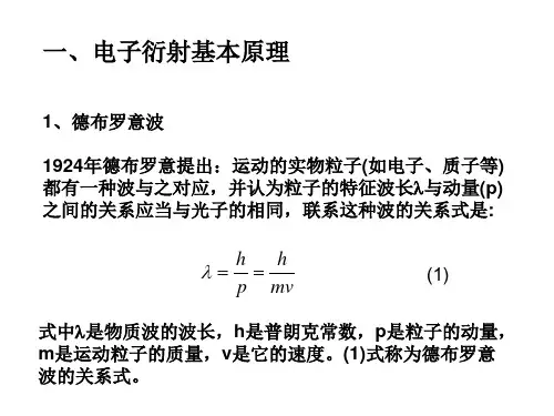


新开近代物理实验讲义之七 -----电子衍射实验讲义一 实验目的1 验证电子具有波动性的假设;2 了解电子衍射和电子衍射实验对物理学发展的意义;3 了解电子衍射在研究晶体结构中的应用; 二 实验仪器电子衍射,真空机组,复合真空计,数码相机,微机 三 实验原理 (一)、电子的波粒二象性波在传播过程中遇到障碍物时会绕过障碍物继续传播,在经典物理学中称为波的衍射,光在传播过程表现出波的衍射性,光还表现出干涉和偏振现象,表明光有波动性;光电效应揭示光与物质相互作用时表现出粒子性,其能量有一个不能连续分割的最小单元,即普朗克1900年首先作为一个基本假设提出来的普朗克关系hv E =E 为光子的能量,v 为光的频率,h 为普朗克常数,光具有波粒二象性。
电子在与电磁场相互作用时表现为粒子性,在另一些相互作用过程中是否会表现出波动性?德布罗意从光的波粒二象性得到启发,在1923-1924年间提出电子具有波粒二象性的假设,k p E==,ωE 为电子的能量,p为电子的动量,v πω2=为平面波的圆频率,k 为平面波的波矢量,π2/h = 为约化普朗克常数;波矢量的大小与波长λ的关系为λπ/2=k ,k p=称为德布罗意关系。
电子具有波粒二象性的假设,拉开了量子力学革命的序幕。
电子具有波动性假设的实验验证是电子的晶体衍射实验。
电子被电场加速后,电子的动能等于电子的电荷乘加速电压,即eV E k =考虑到高速运动的相对论效应,电子的动量)2(12mc E E cp k +=λ 由德布罗意关系得)2/1(222mc E E mc hck k +=λ真空中的光速s A c o/1099793.218⨯=,电子的静止质量26/10511.0c eV m ⨯=,普朗克常数eV A hc eVs h o4151023986.1,1013571.4⨯=⨯=-,当电子所受的加速电压为V 伏特,则电子的动能VeV E k =,电子的德布罗意波长o A V V)1089.41(1507-⨯-≈λ, (1)加速电压为100伏特,电子的德布罗意波长为oA 225.1。