ST7920控制器的lcd12864驱动程序头文件+6页+0[1].1M
- 格式:pdf
- 大小:72.90 KB
- 文档页数:6
![ST7920控制器的lcd12864驱动程序头文件+6页+0[1].1M](https://img.taocdn.com/s1/m/5fb6941155270722192ef7bf.png)
完整功能版的ST7920驱动的12864液晶(并行驱动),MCU= Mega162007-07-04 23:40:11| 分类:AVR单片机| 标签:avr |字号大中小订阅/**************************************************** 工程:ST7920驱动的12864液晶的并行驱动模式创建日期:2007年7月3日创建人:朱海峰邮箱:ntzhf100@ QQ:543376422 引脚定义:RS(CS)=====>PB0RW(SID)====>PB1EN(SCLK)===>PB2D0=========>PA0::D7=========>PA7PSB为硬件控制,接高电平为8位或4位的并行模式,接低电平为串行模式****************************************************/#include <iom16v.h>#include <macros.h>#define uint8_t unsigned char#define uint16_t unsigned int#define nop() NOP()#define DATA_PORT PORTA#define Set_RS() DDRB |= (1<<0);PORTB |= (1<<0);#define Set_RW() DDRB |= (1<<1);PORTB |= (1<<1);#define Set_EN() DDRB |= (1<<2);PORTB |= (1<<2);#define Clr_RS() DDRB |= (1<<0);PORTB &= ~(1<<0);#define Clr_RW() DDRB |= (1<<1);PORTB &= ~(1<<1);#define Clr_EN() DDRB |= (1<<2);PORTB &= ~(1<<2);#define Set_output() DDRA = 0XFF#define Set_input() DDRA = 0X00#define PIN_port PINA#define left 0x18#define right 0x1c#define xtal 8 //晶振调整MHzvoid WriteCom(uint8_t CMD);void WriteDat(uint8_t DAT);void Delay(uint16_t ms);uint8_t CheckBusy(void);void Draw_Pic(uint8_t x, uint8_t y, const uint8_t *Draw);void Picture_Set_XY(uint8_t x, uint8_t y);void Char_Set_XY(uint8_t x, uint8_t y, uint8_t *p);void Lcd_Init(void);void Chip_Init(void);void Set_Draw(void);void Lcd_flash(uint16_t delay_t,uint8_t times);void Move(uint8_t step,uint8_t dirction,uint16_t time);const uint8_t PIC1[64][16]={/*-- 调入了一幅图像:C:\Documents and Settings\Administrator\桌面\atmel.bmp --*//*-- 宽度x高度=128x64 --*/0x00,0x00,0x00,0x00,0x00,0x00,0x00,0x00,0x00,0x00,0x00,0x00,0x00,0x00,0x00,0x0 0,0x00,0x00,0x00,0x00,0x00,0x00,0x00,0x00,0x00,0x00,0x00,0x00,0x00,0x00,0x00,0x0 0,0x00,0x00,0x00,0x00,0x00,0x00,0x00,0x00,0x00,0x00,0x00,0x00,0x00,0x00,0x00,0x00x00,0x00,0x00,0x00,0x00,0x00,0x00,0x00,0x00,0x00,0x00,0x00,0x00,0x00,0x00,0x0 0,0x00,0x00,0x00,0x00,0x00,0x00,0x00,0x00,0x00,0x00,0x00,0x00,0x00,0x00,0x00,0x0 0,0x00,0x00,0x00,0x00,0x00,0x00,0x00,0x00,0x00,0x00,0x00,0x00,0x00,0x00,0x00,0x0 0,0x00,0x00,0x00,0x7F,0xFF,0xFF,0xFF,0xFF,0xFF,0xFF,0xFF,0xFF,0xFF,0xFC,0x00,0x00, 0x00,0x00,0x00,0xFF,0xFF,0xFF,0xFF,0xFF,0xFF,0xFF,0xFF,0xFF,0xFF,0xFC,0x00,0x00, 0x00,0x00,0x00,0xFF,0xFF,0xFF,0xFF,0xFF,0xFF,0xFF,0xFF,0xFF,0xFF,0xFC,0x00,0x00, 0x00,0x00,0x01,0xFF,0xFF,0xFF,0xFF,0xFF,0xFF,0xFF,0xFF,0xFF,0xFF,0xFC,0x00,0x00, 0x00,0x00,0x03,0xFF,0xFF,0xFF,0xFF,0xFF,0xFF,0xFF,0xFF,0xFF,0xFF,0xFC,0x00,0x00, 0x00,0x00,0x03,0xFF,0xFF,0xFF,0xFF,0xFF,0xFF,0xFF,0xFF,0xFF,0xFF,0xFC,0x00,0x00, 0x00,0x00,0x07,0xFF,0xFF,0xFF,0xFF,0xFF,0xFF,0xFF,0xFF,0xFF,0xFF,0xFC,0x00,0x00, 0x00,0x00,0x07,0xFF,0xFF,0xFF,0xFF,0xFF,0xFF,0xFF,0xFF,0xFF,0xFF,0xFC,0x00,0x00, 0x00,0x00,0x0F,0xFF,0xFF,0xFF,0xFF,0xFF,0xFF,0xFF,0xFF,0xFF,0xFF,0xFC,0x00,0x00, 0x00,0x00,0x0F,0xFF,0xFF,0xFF,0xFF,0xFF,0xFF,0xFF,0xFF,0xFF,0xFF,0xF8,0x00,0x00, 0x00,0x00,0x00,0x07,0xFC,0x00,0x00,0x00,0x00,0x00,0x00,0x00,0x00,0x00,0x00,0x0 0,0x00,0x00,0x00,0x07,0xFC,0x00,0x00,0x00,0x00,0x00,0x00,0x00,0x00,0x00,0x00,0x0 0,0x00,0x00,0x3F,0xE7,0xFC,0xFF,0xFF,0xFF,0xE0,0xFF,0xFF,0xCF,0xF8,0x00,0x00,0x00,0x00,0x00,0x3F,0xE7,0xFC,0xFF,0xFF,0xFF,0xF0,0xFF,0xFF,0xCF,0xF8,0x00,0x00,0x00, 0x00,0x00,0x7F,0xE7,0xFC,0xFF,0xFF,0xFF,0xF8,0xFF,0xFF,0xCF,0xF8,0x00,0x00,0x00, 0x00,0x00,0x7F,0xE7,0xFC,0xFF,0xFF,0xFF,0xFC,0xFF,0xFF,0xCF,0xF8,0x00,0x00,0x00, 0x00,0x00,0xFF,0xE7,0xFC,0xFF,0xBF,0xEF,0xFC,0xFF,0xFF,0xCF,0xF8,0x00,0x00,0x00, 0x00,0x00,0xFF,0xE7,0xFC,0xFF,0xBF,0xE7,0xFC,0xFF,0xFF,0xCF,0xF8,0x00,0x00,0x00, 0x00,0x01,0xFF,0xE7,0xFC,0xFF,0xBF,0xE7,0xFC,0xFF,0xFF,0xCF,0xF8,0x00,0x00,0x00, 0x00,0x03,0xFF,0xE7,0xFC,0xFF,0xBF,0xE7,0xFC,0xFF,0xFF,0xCF,0xF8,0x00,0x00,0x00, 0x00,0x03,0xFF,0xE7,0xFC,0xFF,0xBF,0xE7,0xFC,0xFF,0xFF,0xCF,0xF8,0x00,0x00,0x00, 0x00,0x07,0xFF,0xE7,0xFC,0xFF,0xBF,0xE7,0xFC,0xFC,0x00,0x0F,0xF8,0x00,0x00,0x00, 0x00,0x07,0xFF,0xE7,0xFC,0xFF,0xBF,0xE7,0xFC,0xFF,0xFF,0xCF,0xF8,0x00,0x00,0x00, 0x00,0x0F,0xFF,0xE7,0xFC,0xFF,0xBF,0xE7,0xFC,0xFF,0xFF,0xCF,0xF8,0x00,0x00,0x00, 0x00,0x0F,0xFF,0xE7,0xFC,0xFF,0xBF,0xE7,0xFC,0xFF,0xFF,0xCF,0xF8,0x00,0x00,0x00, 0x00,0x1F,0xFF,0xE7,0xFC,0xFF,0xBF,0xE7,0xFC,0xFF,0xFF,0xCF,0xF8,0x00,0x00,0x00, 0x00,0x1F,0xFF,0xE7,0xFC,0xFF,0xBF,0xE7,0xFC,0xFF,0xFF,0xCF,0xF8,0x00,0x00,0x00, 0x00,0x3F,0xFF,0xE7,0xFC,0xFF,0xBF,0xE7,0xFC,0xFF,0xFF,0xCF,0xF8,0x00,0x00,0x00, 0x00,0x3F,0xFF,0xE7,0xFC,0xFF,0xBF,0xE7,0xFC,0xFF,0xFF,0xCF,0xF8,0x00,0x00,0x00, 0x00,0x7F,0xFF,0xE7,0xFC,0xFF,0xBF,0xE7,0xFC,0xFF,0xFF,0xCF,0xF8,0x00,0x00,0x00, 0x00,0xFF,0xFF,0xE7,0xFC,0xFF,0xBF,0xE7,0xFC,0xFF,0xFF,0xCF,0xF8,0x00,0x00,0x00, 0x00,0xFF,0xFF,0xE7,0xFC,0xFF,0xBF,0xE7,0xFC,0xFC,0x00,0x0F,0xF8,0x00,0x00,0x00, 0x01,0xFF,0xBF,0xE7,0xFC,0xFF,0xBF,0xE7,0xFC,0xFE,0x00,0x0F,0xF8,0x00,0x00,0x00, 0x01,0xFF,0x3F,0xE7,0xFC,0xFF,0xBF,0xE7,0xFC,0xFF,0xFF,0xCF,0xFF,0xF8,0x00,0x00, 0x03,0xFF,0x3F,0xE7,0xFC,0xFF,0xBF,0xE7,0xFC,0xFF,0xFF,0xCF,0xFF,0xF8,0x00,0x00,0x03,0xFE,0x3F,0xE7,0xFC,0xFF,0xBF,0xE7,0xFC,0xFF,0xFF,0xCF,0xFF,0xF0,0x00,0x00, 0x07,0xFE,0x3F,0xE7,0xFC,0xFF,0xBF,0xE7,0xFC,0xFF,0xFF,0xCF,0xFF,0xF0,0x00,0x00, 0x07,0xFF,0x3F,0xE7,0xFC,0xFF,0xBF,0xE7,0xFC,0xFF,0xFF,0xCF,0xFF,0xE0,0x00,0x00, 0x0F,0xFF,0x3F,0xE7,0xFC,0xFF,0xBF,0xE7,0xFC,0xFF,0xFF,0xCF,0xFF,0xE0,0x00,0x00, 0x0F,0xFF,0x3F,0xE7,0xFC,0xFF,0xBF,0xE7,0xFC,0xFF,0xFF,0xCF,0xFF,0xC0,0x00,0x00, 0x1F,0xFF,0x3F,0xE7,0xFC,0xFF,0xBF,0xE7,0xFC,0xFF,0xFF,0xCF,0xFF,0xC0,0x00,0x00, 0x1F,0xFF,0x3F,0xE7,0xFC,0xFF,0x1F,0xE7,0xFC,0xFF,0xFF,0xCF,0xFF,0x80,0x00,0x00, 0x00,0x00,0x00,0x00,0x00,0x00,0x00,0x00,0x00,0x00,0x00,0x00,0x00,0x00,0x00,0x0 0,0x1F,0xFF,0xFF,0xFF,0xFF,0xFF,0xFF,0xFF,0xFF,0xFF,0xFF,0xFF,0xFF,0x3E,0x00,0x00,0x1F,0xFF,0xFF,0xFF,0xFF,0xFF,0xFF,0xFF,0xFF,0xFF,0xFF,0xFF,0xFF,0x63,0x00,0x00,0x1F,0xFF,0xFF,0xFF,0xFF,0xFF,0xFF,0xFF,0xFF,0xFF,0xFF,0xFF,0xFE,0xFD,0x00,0x00, 0x1F,0xFF,0xFF,0xFF,0xFF,0xFF,0xFF,0xFF,0xFF,0xFF,0xFF,0xFF,0xFC,0xB6,0x80,0x00, 0x1F,0xFF,0xFF,0xFF,0xFF,0xFF,0xFF,0xFF,0xFF,0xFF,0xFF,0xFF,0xFC,0xBE,0x80,0x00, 0x1F,0xFF,0xFF,0xFF,0xFF,0xFF,0xFF,0xFF,0xFF,0xFF,0xFF,0xFF,0xF8,0xB6,0x80,0x00, 0x1F,0xFF,0xFF,0xFF,0xFF,0xFF,0xFF,0xFF,0xFF,0xFF,0xFF,0xFF,0xF8,0xF7,0x00,0x00, 0x1F,0xFF,0xFF,0xFF,0xFF,0xFF,0xFF,0xFF,0xFF,0xFF,0xFF,0xFF,0xF0,0x63,0x00,0x00, 0x00,0x00,0x00,0x00,0x00,0x00,0x00,0x00,0x00,0x00,0x00,0x00,0x00,0x3C,0x00,0x0 0,0x00,0x00,0x00,0x00,0x00,0x00,0x00,0x00,0x00,0x00,0x00,0x00,0x00,0x00,0x00,0x0 0,0x00,0x00,0x00,0x00,0x00,0x00,0x00,0x00,0x00,0x00,0x00,0x00,0x00,0x00,0x00,0x00,0x00,0x00,0x00,0x00,0x00,0x00,0x00,0x00,0x00,0x00,0x00,0x00,0x00,0x00,0x00,0x0 0,0x00,0x00,0x00,0x00,0x00,0x00,0x00,0x00,0x00,0x00,0x00,0x00,0x00,0x00,0x00,0x0 0,0x00,0x00,0x00,0x00,0x00,0x00,0x00,0x00,0x00,0x00,0x00,0x00,0x00,0x00,0x00,0x0 0,0x00,0x00,0x00,0x00,0x00,0x00,0x00,0x00,0x00,0x00,0x00,0x00,0x00,0x00,0x00,0x0 0};const uint8_t PIC2[64][16]={/*-- 调入了一幅图像:C:\Documents and Settings\Administrator\桌面\AVR.BMP --*//*-- 宽度x高度=128x64 --*/0x00,0x00,0x00,0x00,0x00,0x00,0x00,0x00,0x00,0x00,0x00,0x00,0x00,0x00,0x00,0x0 0,0x00,0x00,0x00,0x00,0x00,0x00,0x00,0x00,0x00,0x00,0x00,0x00,0x00,0x00,0x00,0x0 0,0x00,0x00,0x00,0x00,0x00,0x00,0x00,0x00,0x00,0x00,0x00,0x00,0x00,0x00,0x00,0x3 C,0x00,0x00,0x00,0x00,0x00,0x00,0x00,0x00,0x00,0x00,0x00,0x00,0x00,0x00,0x00,0x4 3,0x00,0x00,0x00,0x00,0x00,0x00,0x00,0x00,0x00,0x00,0x00,0x00,0x00,0x00,0x00,0xB D,0x00,0x00,0x00,0x00,0x00,0x00,0x00,0x00,0x00,0x00,0x00,0x00,0x00,0x00,0x01,0x2 7,0x00,0x00,0x1F,0xFF,0x83,0xFF,0xE0,0x00,0x00,0xFF,0xF8,0x3F,0xFF,0xFF,0x01,0x3C, 0x00,0x00,0x3F,0xFF,0x81,0xFF,0xF0,0x00,0x01,0xFF,0xF0,0x7F,0xFF,0xFF,0xC1,0x3E, 0x00,0x00,0x3F,0xFF,0xC1,0xFF,0xF0,0x00,0x01,0xFF,0xF0,0x7F,0xFF,0xFF,0xE0,0xA7, 0x00,0x00,0x3F,0xFF,0xC1,0xFF,0xF0,0x00,0x03,0xFF,0xE0,0x7F,0xFF,0xFF,0xF0,0xE7, 0x00,0x00,0x7F,0xFF,0xE0,0xFF,0xF8,0x00,0x03,0xFF,0xE0,0xFF,0xFF,0xFF,0xF8,0x7E, 0x00,0x00,0x7F,0xFF,0xE0,0xFF,0xF8,0x00,0x03,0xFF,0xE0,0xFF,0xFF,0xFF,0xF8,0x00, 0x00,0x00,0x7F,0xFF,0xE0,0x7F,0xFC,0x00,0x07,0xFF,0xC1,0xFF,0xFF,0xFF,0xFC,0x00, 0x00,0x00,0xFF,0xFF,0xF0,0x7F,0xFC,0x00,0x07,0xFF,0xC1,0xFF,0xFF,0xFF,0xFC,0x00, 0x00,0x00,0xFF,0xFF,0xF0,0x7F,0xFE,0x00,0x0F,0xFF,0x83,0xFF,0xFF,0xFF,0xFE,0x00, 0x00,0x01,0xFF,0xFF,0xF8,0x3F,0xFE,0x00,0x0F,0xFF,0x83,0xFF,0xE0,0x7F,0xFE,0x00, 0x00,0x01,0xFF,0xFF,0xF8,0x3F,0xFE,0x00,0x1F,0xFF,0x07,0xFF,0xC0,0x3F,0xFE,0x00, 0x00,0x03,0xFF,0xFF,0xF8,0x3F,0xFF,0x00,0x1F,0xFF,0x07,0xFF,0xC0,0x3F,0xFE,0x00, 0x00,0x03,0xFF,0xFF,0xFC,0x1F,0xFF,0x00,0x1F,0xFE,0x07,0xFF,0xC0,0x3F,0xFE,0x00, 0x00,0x03,0xFF,0xFF,0xFC,0x1F,0xFF,0x80,0x3F,0xFE,0x0F,0xFF,0x80,0x3F,0xFE,0x00, 0x00,0x07,0xFF,0xFF,0xFE,0x0F,0xFF,0x80,0x3F,0xFE,0x0F,0xFF,0x80,0x3F,0xFE,0x00, 0x00,0x07,0xFF,0x9F,0xFE,0x0F,0xFF,0x80,0x7F,0xFC,0x1F,0xFF,0x00,0x7F,0xFE,0x00, 0x00,0x07,0xFF,0x9F,0xFF,0x07,0xFF,0xC0,0x7F,0xFC,0x1F,0xFF,0x00,0xFF,0xFC,0x00, 0x00,0x0F,0xFF,0x8F,0xFF,0x07,0xFF,0xC0,0x7F,0xF8,0x1F,0xFF,0x01,0xFF,0xFC,0x00,0x00,0x0F,0xFF,0x0F,0xFF,0x03,0xFF,0xC0,0xFF,0xF8,0x3F,0xFF,0xFF,0xFF,0xF8,0x00, 0x00,0x0F,0xFF,0x0F,0xFF,0x83,0xFF,0xE0,0xFF,0xF8,0x3F,0xFF,0xFF,0xFF,0xF8,0x00, 0x00,0x1F,0xFF,0x07,0xFF,0x83,0xFF,0xE1,0xFF,0xF0,0x7F,0xFF,0xFF,0xFF,0xF0,0x00, 0x00,0x1F,0xFE,0x07,0xFF,0xC1,0xFF,0xF1,0xFF,0xF0,0x7F,0xFF,0xFF,0xFF,0xE0,0x00, 0x00,0x3F,0xFE,0x07,0xFF,0xC1,0xFF,0xF3,0xFF,0xE0,0x7F,0xFF,0xFF,0xFF,0xC0,0x00, 0x00,0x3F,0xFE,0x03,0xFF,0xC0,0xFF,0xFB,0xFF,0xE0,0xFF,0xFF,0xFF,0xFF,0x80,0x00, 0x00,0x7F,0xFC,0x03,0xFF,0xE0,0xFF,0xFB,0xFF,0xC0,0xFF,0xFF,0xFF,0xFF,0x00,0x00, 0x00,0x7F,0xFC,0x03,0xFF,0xE0,0x7F,0xFF,0xFF,0xC1,0xFF,0xFF,0xFF,0xFC,0x00,0x00, 0x00,0x7F,0xF8,0x01,0xFF,0xF0,0x7F,0xFF,0xFF,0x81,0xFF,0xFF,0xFF,0xE0,0x00,0x00, 0x00,0xFF,0xFF,0xFF,0xFF,0xF8,0x3F,0xFF,0xFF,0x83,0xFF,0xFF,0xFF,0xC0,0x00,0x00, 0x00,0xFF,0xFF,0xFF,0xFF,0xF8,0x3F,0xFF,0xFF,0x83,0xFF,0xF3,0xFF,0xC0,0x00,0x00, 0x00,0xFF,0xFF,0xFF,0xFF,0xF8,0x3F,0xFF,0xFF,0x03,0xFF,0xE3,0xFF,0xE0,0x00,0x00, 0x01,0xFF,0xFF,0xFF,0xFF,0xFC,0x1F,0xFF,0xFF,0x07,0xFF,0xE3,0xFF,0xE0,0x00,0x00, 0x01,0xFF,0xFF,0xFF,0xFF,0xFC,0x1F,0xFF,0xFE,0x07,0xFF,0xC3,0xFF,0xE0,0x00,0x00, 0x03,0xFF,0xFF,0xFF,0xFF,0xFE,0x1F,0xFF,0xFE,0x0F,0xFF,0xC1,0xFF,0xF0,0x00,0x00, 0x03,0xFF,0xFF,0xFF,0xFF,0xFE,0x0F,0xFF,0xFE,0x0F,0xFF,0x81,0xFF,0xF0,0x00,0x00, 0x03,0xFF,0xFF,0xFF,0xFF,0xFE,0x0F,0xFF,0xFC,0x0F,0xFF,0x81,0xFF,0xF8,0x00,0x00, 0x07,0xFF,0xFF,0xFF,0xFF,0xFF,0x07,0xFF,0xFC,0x1F,0xFF,0x81,0xFF,0xF8,0x00,0x00, 0x07,0xFF,0xFF,0xFF,0xFF,0xFF,0x07,0xFF,0xF8,0x3F,0xFF,0x00,0xFF,0xF8,0x00,0x00, 0x0F,0xFF,0xC0,0x00,0x1F,0xFF,0x83,0xFF,0xF8,0x3F,0xFF,0x00,0xFF,0xF8,0x00,0x00, 0x0F,0xFF,0x80,0x00,0x0F,0xFF,0x83,0xFF,0xF0,0x3F,0xFE,0x00,0xFF,0xFC,0x00,0x00, 0x0F,0xFF,0x80,0x00,0x0F,0xFF,0xC3,0xFF,0xF0,0x7F,0xFE,0x00,0x7F,0xFC,0x00,0x00,0x1F,0xFF,0x00,0x00,0x0F,0xFF,0xC1,0xFF,0xF0,0x7F,0xFC,0x00,0x7F,0xFC,0x00,0x00, 0x1F,0xFF,0x00,0x00,0x07,0xFF,0xC1,0xFF,0xE0,0x7F,0xFC,0x00,0x7F,0xFE,0x00,0x00, 0x1F,0xFF,0x00,0x00,0x07,0xFF,0xE0,0xFF,0xE0,0xFF,0xF8,0x00,0x7F,0xFE,0x00,0x00, 0x3F,0xFE,0x00,0x00,0x03,0xFF,0xE0,0xFF,0xC0,0xFF,0xF8,0x00,0x3F,0xFE,0x00,0x00, 0x00,0x00,0x00,0x00,0x00,0x00,0x00,0x7F,0xC0,0x00,0x00,0x00,0x00,0x00,0x00,0x0 0,0x00,0x00,0x00,0x00,0x00,0x00,0x00,0x7F,0xC0,0x00,0x00,0x00,0x00,0x00,0x00,0x0 0,0x00,0x00,0x00,0x00,0x00,0x00,0x00,0x7F,0x80,0x00,0x00,0x00,0x00,0x00,0x00,0x0 0,0x00,0x00,0x00,0x00,0x00,0x00,0x00,0x3F,0x00,0x00,0x00,0x00,0x00,0x00,0x00,0x0 0,0x00,0x00,0x00,0x00,0x00,0x00,0x00,0x3F,0x00,0x00,0x00,0x00,0x00,0x00,0x00,0x0 0,0x00,0x00,0x00,0x00,0x00,0x00,0x00,0x1F,0x00,0x00,0x00,0x00,0x00,0x00,0x00,0x0 0,0x00,0x00,0x00,0x00,0x00,0x00,0x00,0x1E,0x00,0x00,0x00,0x00,0x00,0x00,0x00,0x0 0,0x00,0x00,0x00,0x00,0x00,0x00,0x00,0x0E,0x00,0x00,0x00,0x00,0x00,0x00,0x00,0x0 0,0x00,0x00,0x00,0x00,0x00,0x00,0x00,0x0C,0x00,0x00,0x00,0x00,0x00,0x00,0x00,0x0 0,0x00,0x00,0x00,0x00,0x00,0x00,0x00,0x0C,0x00,0x00,0x00,0x00,0x00,0x00,0x00,0x0 0,0x00,0x00,0x00,0x00,0x00,0x00,0x00,0x00,0x00,0x00,0x00,0x00,0x00,0x00,0x00,0x0 0,0x00,0x00,0x00,0x00,0x00,0x00,0x00,0x00,0x00,0x00,0x00,0x00,0x00,0x00,0x00,0x0 0,0x00,0x00,0x00,0x00,0x00,0x00,0x00,0x00,0x00,0x00,0x00,0x00,0x00,0x00,0x00,0x0 0,0x00,0x00,0x00,0x00,0x00,0x00,0x00,0x00,0x00,0x00,0x00,0x00,0x00,0x00,0x00,0x0 0};/**************************************************/void main(void){uint8_t i;Delay(10);Chip_Init(); //芯片初始化函数Lcd_Init(); //液晶初始化函数while(1)//ST7920的好处就是带字库,所以程序里可以直接写中英文和字符{ //英文和字符为半角的Char_Set_XY(0,0,"ntzhf100@"); //在第0行的第0个位置依次输出文字Char_Set_XY(2,1,"蓝水天下"); //在第1行的第2个位置依次输出文字Char_Set_XY(0,2,"我的天下,我的自"); //在第2行的第0个位置依次输出文字Char_Set_XY(0,3,"由空间!"); //在第3行的第0个位置依次输出文字Delay(2000); //软件延时2SLcd_flash(500,3); //液晶闪烁程序每次500ms的延时,闪动3次//=========液晶内部的地址=============//Line1 80H 81H 82H 83H 84H 85H 86H 87H//Line2 90H 91H 92H 93H 94H 95H 96H 97H//Line3 88H 89H 8AH 8BH 8CH 8DH 8EH 8FH//Line4 98H 99H 9AH 9BH 9CH 9DH 9EH 9FH//因为液晶本身的缺陷,所以移动显示会很丑Move(8,left,500); //液晶左移程序,移动8步,步与步之间间隔500ms Delay(2000); //软件延时2SMove(8,right,500); //液晶右移程序,移动8步,步与步之间间隔500ms Delay(2000); //软件延时2SSet_Draw(); //设定为绘图模式Draw_Pic(0,0,*PIC1); //第一张图片ATMEL的LOGODelay(3000); //软件延时3SDraw_Pic(0,0,*PIC2); //第一张图片AVR的LOGODelay(3000); //软件延时3SLcd_Init(); //重新设定为普通模式,即输出中英文和字符模式}}/*************************************************/ void Chip_Init(void){DDRA = 0XFF;PORTA = 0X00;DDRB = 0X07;PORTB = 0X00;}/*************************************************/ void Lcd_Init(void){uint8_t cmd;cmd=0x30; //功能设置8位数据,基本指令WriteCom(cmd); //写指令cmd=0x0C; //显示状态ON,游标OFF,反白OFF WriteCom(cmd); //写指令cmd=0x01; //清除显示WriteCom(cmd); //写指令cmd=0x02; //地址归位WriteCom(cmd); //写指令cmd=0x80; //设置DDRAM地址WriteCom(cmd); //写指令Delay(100); //延时}/*************************************************/void Delay(uint16_t ms) //毫秒级延时,当改晶振为几M则xtal设为几{uint16_t i;while(ms--){for(i=1;i<(uint16_t)(xtal*143-2);i++);}}/*************************************************/void Lcd_flash(uint16_t delay_t,uint8_t times){uint8_t j;for(j=0;j<times;j++){WriteCom(0x08); //关闭显示Delay(delay_t); //软件延时WriteCom(0x0c); //开显示Delay(delay_t); //软件延时}}/*************************************************/ void Move(uint8_t step,uint8_t dirction,uint16_t time) {uint8_t i;for(i=0;i<step-1;i++) //移动的步数{WriteCom(dirction); //文字移动方向Delay(time); //控制移动时间}}/*************************************************/ void WriteCom(uint8_t CMD) //写控制命令函数{while(CheckBusy()); //检测液晶内部是否忙Clr_RS();Clr_RW();DATA_PORT = CMD;Set_EN();nop();nop();}/*************************************************/ void WriteDat(uint8_t DAT) //写数据函数{while(CheckBusy()); //检测液晶内部是否忙Set_RS();Clr_RW();DATA_PORT = DAT;Set_EN();nop();nop();Clr_EN();}/*************************************************/ uint8_t CheckBusy(void){uint8_t temp;DATA_PORT = 0XFF;Clr_RS();nop(); //这里的nop不能省略,否则不行Set_RW();Set_EN();nop();Set_input();nop();temp = PINA;nop();Clr_EN();nop();Set_output();temp &= 0x80;return(temp);}/*************************************************/ void Char_Set_XY(uint8_t x, uint8_t y, uint8_t *p) {if(y == 0){WriteCom((0x80+x));}if(y == 1){WriteCom((0x90+x));}if(y == 2){WriteCom((0x88+x));}if(y == 3){WriteCom((0x98+x));}while(*p != 0){WriteDat(*p++);}}/*************************************************/void Set_Draw(void){WriteCom(0x01); //清屏Delay(20); //延时WriteCom(0x36); //8BIT控制界面,扩充指令集,,绘图显示ON Delay(20); //延时}/*************************************************/ void Draw_Pic(uint8_t x, uint8_t y, const uint8_t *Draw) {uint8_t i, j, temp_x, temp_y;temp_x = x;temp_y = y;temp_x |= 0x80;temp_y |= 0x80;for(i=0;i<32;i++ ){WriteCom(temp_y++); //设置绘图区的Y地址坐标WriteCom(temp_x); //设置绘图区的X地址坐标for(j=0;j<16;j++){WriteDat(*Draw);Draw++;}}temp_x = 0x88;temp_y = 0x80;j = 0;for(;i<64;i++ ){WriteCom(temp_y++); //设置绘图区的Y地址坐标WriteCom(temp_x); //设置绘图区的X地址坐标for(j=0;j<16;j++){WriteDat(*Draw);Draw++;}}}/**************************************************/12864串行/*************************************** start51 study board test software** test 12864LCD** using serial interface** author:bluehacker<kernelpaniccrash AT > ** QQ:282074921** Date:2007-11-18**************************************/#ifndef _LZP_START51_12864LCDS_H#define _LZP_START51_12864LCDS_H#include "reg52.h"//12864串行口定义sbit LCD_CS=P2^3;sbit LCD_CLK=P2^5;sbit LCD_SID=P2^4;//12864LCD指令定义#define CMD_CLEAR 0x01#define CMD_RESET 0x02//设置波特率#define OSC_FREQ 11059200L#define BAUD_115200 256 - (OSC_FREQ/192L)/115200L // 255 #define BAUD_57600 256 - (OSC_FREQ/192L)/57600L // 254 #define BAUD_38400 256 - (OSC_FREQ/192L)/38400L // 253 #define BAUD_28800 256 - (OSC_FREQ/192L)/28800L // 252 #define BAUD_19200 256 - (OSC_FREQ/192L)/19200L // 250 #define BAUD_14400 256 - (OSC_FREQ/192L)/14400L // 248 #define BAUD_9600 256 - (OSC_FREQ/192L)/9600L // 244 void Delay_us(unsigned char nUs);void Delay_ms(unsigned int nMs);bit lcd_busy(void);void write_command(unsigned char cmd);unsigned char read_data(void);void write_data(unsigned char dat);void clear_lcd();void lcd_init();void lcd_setxy(unsigned char x,unsigned char y);void lcd_display_str(unsigned char x, unsigned char y,unsigned char *str);#endif我的是ST7920控制的.接了RS(CS),与WR(SID)两个至单片机,节约了串口.另外PSB(串行为0,并行接1)跟LED-接GND,RS与LED+接VCC.这个程序可能还有点问题,接上背光(LED+,LED-)显示就不很清晰了,关了之后很清晰. 显示最后三个汉字"李正平"错误,为"李掌"可笑.查查程序哪里有问题了//FileName:12864lcds.c/*************************************** start51 study board test software** test 12864LCD** using serial interface** author:bluehacker<kernelpaniccrash AT > ** QQ:282074921** Date:2007-11-18**************************************/#include "12864.h"void Delay_us(unsigned char nUs){unsigned char i;while(nUs--)for(i=0;i<10;i++);}void Delay_ms(unsigned int nMs){ unsigned char i;while(nMs--)for(i=0;i<120;i++);}bit lcd_busy(){unsigned char i;bit dat;//先产生连续5个'1'LCD_CS=1;for(i=0;i<5;i++){LCD_CLK=0;LCD_SID=1;LCD_CLK=1;}//再发送一个'1',表示读操作LCD_CLK=0;LCD_SID=1;LCD_CLK=1;//再发送一个'0',表示写命令操作LCD_CLK=0;LCD_SID=0;LCD_CLK=1;//再发送一个'0',这是表示第一个字节结束LCD_CLK=0;LCD_SID=0;LCD_CLK=1;//Delay_us(1);dat=0;LCD_CLK=0;dat=LCD_SID;LCD_CLK=1;LCD_CS=0;return dat;}void write_command(unsigned char cmd) {unsigned char i;while(lcd_busy());//先产生连续5个'1'LCD_CS=1;for(i=0;i<5;i++){LCD_CLK=0;LCD_SID=1;LCD_CLK=1;}//再发送一个'0',表示写操作LCD_CLK=0;LCD_SID=0;LCD_CLK=1;//再发送一个'0',表示写命令操作LCD_CLK=0;LCD_SID=0;LCD_CLK=1;//再发送一个'0',这是表示第一个字节结束LCD_CLK=0;LCD_SID=0;LCD_CLK=1;//下面发送具体指令,先发送高4位for(i=0;i<4;i++){LCD_CLK=0;if(cmd&0x80)LCD_SID=1;elseLCD_SID=0;LCD_CLK=1;cmd<<=1;}//发送连续4个'0'for(i=0;i<4;i++){LCD_CLK=0;LCD_SID=0;LCD_CLK=1;}//下面发送指令的低4位for(i=0;i<4;i++){LCD_CLK=0;if(cmd&0x80)LCD_SID=1;elseLCD_SID=0;LCD_CLK=1;cmd<<=1;}//发送连续4个'0'for(i=0;i<4;i++){LCD_CLK=0;LCD_SID=0;LCD_CLK=1;}LCD_CS=0;//结束}void write_data(unsigned char dat) {unsigned char i;while(lcd_busy());//先产生连续5个'1'LCD_CS=1;for(i=0;i<5;i++){LCD_CLK=0;LCD_SID=1;LCD_CLK=1;}//再发送一个'0',表示写操作LCD_CLK=0;LCD_SID=0;LCD_CLK=1;//再发送一个'1',表示写数据操作LCD_CLK=0;LCD_SID=1;LCD_CLK=1;//再发送一个'0',这是表示第一个字节结束LCD_CLK=0;LCD_SID=0;LCD_CLK=1;//下面发送具体数据,先发送高4位for(i=0;i<4;i++){LCD_CLK=0;if(dat&0x80)LCD_SID=1;elseLCD_SID=0;LCD_CLK=1;dat<<=1;}//发送连续4个'0'for(i=0;i<4;i++){LCD_CLK=0;LCD_SID=0;LCD_CLK=1;}//下面发送数据的低4位for(i=0;i<4;i++){LCD_CLK=0;if(dat&0x80)LCD_SID=1;elseLCD_SID=0;LCD_CLK=1;dat<<=1;}//发送连续4个'0'for(i=0;i<4;i++){LCD_CLK=0;LCD_SID=0;LCD_CLK=1;}LCD_CS=0;//结束}unsigned char read_data() {unsigned char i,dat;while(lcd_busy());//先产生连续5个'1'LCD_CS=1;for(i=0;i<5;i++){LCD_CLK=0;LCD_SID=1;LCD_CLK=1;}//再发送一个'1',表示读操作LCD_CLK=0;LCD_SID=0;LCD_CLK=1;//再发送一个'1',表示数据操作LCD_CLK=0;LCD_SID=1;LCD_CLK=1;//再发送一个'0',这是表示第一个字节结束LCD_CLK=0;LCD_SID=0;LCD_CLK=1;//下面读具体数据//先读高4位dat=0;for(i=0;i<4;i++){LCD_CLK=0;dat<<=1;LCD_CLK=1;dat|=LCD_SID;}//再接受4个连续'0',没什么意义,直接丢掉for(i=0;i<4;i++){LCD_CLK=0;Delay_us(1);LCD_CLK=1;Delay_us(1);}//接受低4位for(i=0;i<4;i++){LCD_CLK=0;dat<<=1;LCD_CLK=1;dat|=LCD_SID;}//再接受4个连续'0',没什么意义,直接丢掉for(i=0;i<4;i++){LCD_CLK=0;Delay_us(1);LCD_CLK=1;Delay_us(1);}LCD_CS=0;return dat;}void clear_lcd(){write_command(CMD_CLEAR);}void lcd_setxy(unsigned char x,unsigned char y) {unsigned char addr;switch(y){case 0:addr=0x80+x;break;case 1:addr=0x90+x;break;case 2:addr=0x88+x;break;case 3:addr=0x98+x;break;}write_command(addr);}void lcd_display_str(unsigned char x, unsigned char y,unsigned char *str) {unsigned char i;lcd_setxy(x,y);for(i=0;str[i]!='\0';i++){write_data(str[i]);}}void lcd_init(){write_command(CMD_RESET);write_command(0x0d);//设置显示状态,整体显示ON,游标与游标位置ON write_command(0x30);//功能设置,基本指令write_command(0x18);//游标与显示移位控制clear_lcd();//write_command(0x80);//设置DDRAM位址,并不必须}void main(){TCON=0;SCON=0x50;/*mode 1,1 start bit ,8 data bit ,1 stop bit,enable receive*/ PCON=0x80;/*SMOD=1, Baud Rate twice*/TMOD=0x21;/*timer 0--mode 1 and timer 1 ---mode2*///set baud rate,use timer 1 as baud rate generatorTH1=BAUD_19200;TL1=TH1;TR1=1;// ET1=0;//disable timer 1 interruptEA=0;lcd_init();Delay_ms(100);//显示武林外传lcd_setxy(1,2);write_data(0xce);write_data(0xe4);lcd_setxy(2,2);write_data(0xc1);write_data(0xd6);lcd_setxy(3,2);write_data(0xcd);write_data(0xe2);lcd_setxy(4,2);write_data(0xb4);write_data(0xab);Delay_ms(5000);clear_lcd();write_command(CMD_RESET); Delay_ms(5000);lcd_display_str(2,0,"bluehacker"); lcd_display_str(1,1,"QQ:282074921"); lcd_display_str(3,2,"李正平");LCD12864(ST7920)串行驱动程序作者:L_jeary 文章来源:L_jeary 点击数:286 更新时间:2011-6-23/*==================================================== ================LCD12864对应的C文件,定义了相关的LCD驱动函数主要有:串行驱动LCD12864,内置的控制器为ST7920和ST7921LCD初始化函数读写函数0xf8为写命令的命令字;0xfa为写数据的命令字,这里用的是TI_F28027在编写和调试过程中借鉴了一些网上的程序,在此表示感谢,这里是已经调好的,在移植过程中,调试时注意先要通过示波器对函数void send_data(Uint16 D_Ctrl,Uint16 D_data)的时序检测一下,是否满足要求,不行的话可改一下延时值或者查看硬件是否连好===================================================== ===============*/#include "LCD12864.h" //LCD12864的头文件typedef unsigned int Uint16;/*==================================================== =================管脚的初始化,主要定义复用管脚功能方向等===================================================== =================*/void Init_guanjiao(void){EALLOW;GpioCtrlRegs.GPAMUX2.bit.GPIO16=0;//通用IO 片选CS管脚GpioCtrlRegs.GPADIR.bit.GPIO16=1;//输出GpioCtrlRegs.GPAPUD.bit.GPIO16=1;//禁止上拉电阻GpioCtrlRegs.GPBMUX1.bit.GPIO33=0; //数据管脚SIDGpioCtrlRegs.GPBDIR.bit.GPIO33=1;GpioCtrlRegs.GPBPUD.bit.GPIO33=1;GpioCtrlRegs.GPAMUX1.bit.GPIO2=0;//时钟CLK管脚GpioCtrlRegs.GPADIR.bit.GPIO2=1;GpioCtrlRegs.GPAPUD.bit.GPIO2=1;EDIS;}/*==================================================== =================LCD串行数据传送程序函数名:void send_data(Uint16 D_Ctrl,Uint16 D_data)功能:串行数据传送共分三个字节完成:第一字节:串口控制-格式11111ABCA为数据传送方向控制:H表示数据从LCD到MCU,L表示数据从MCU到LCDB为数据类型选择:H表示数据是显示数据,L表示数据是控制指令C固定为0第二字节分两次传送第一次:(并行)8位数据的高4位-格式DDDD0000 放在一个字节中的高四位第二次:(并行)8位数据的低4位-格式0000DDDD 放在一个字节中的高四位===================================================== =================*/void send_data(Uint16 D_Ctrl,Uint16 D_data)//LCD_CLK一个脉冲写一位{Uint16 i,j;Uint16 temp;//LCD_CS=1; //片选使能GpioDataRegs.GPADAT.bit.GPIO16=1;for(i=0;i<3;i++) // 串行数据的传送{if(i==0) //写第一个字节格式1111 1ABC{temp=D_Ctrl;}if(i==1) //写第二个字节第一次写高四位放在第一次传送的高四位{temp=(D_data&0xf0);}if(i==2) //写第二个字节第二次写低四位放在第二次传送的高四位{temp=(D_data&0x0f);temp=temp<<4;for(j=0;j<8;j++) //串行写8位二进制数据{//LCD_CLK=0; //时钟输入置低GpioDataRegs.GPADAT.bit.GPIO2=0; F_delay(3);if((temp&0x80)==0){//LCD_SID=0; //数据SID GpioDataRegs.GPBDAT.bit.GPIO33=0; }else{//LCD_SID=1; //数据SID GpioDataRegs.GPBDAT.bit.GPIO33=1; }//LCD_CLK=1; //时钟输入置高GpioDataRegs.GPADAT.bit.GPIO2=1; temp=temp<<1;F_delay(5);}//LCD_CLK=0; //时钟输入置低GpioDataRegs.GPADAT.bit.GPIO2=0;//LCD_CS=0; //片选禁止GpioDataRegs.GPADAT.bit.GPIO16=0;}/*==================================================== ===================LCD初始化程序函数名:void lcd_initial()功能:===================================================== ===================*/void lcd_initial(void)//写命令第一字节为0xf8,表示写的是命令//0xfa则表示写数据{Init_guanjiao();send_data(0xf8,0x30); //功能设定//F_delay(10);send_data(0xf8,0x0C); //显示状态开/关//F_delay(10);send_data(0xf8,0x01); //清屏显示//F_delay(10);//send_data(0xf8,0x06); //进如点设定,整体显示设定//F_delay(10);send_data(0xf8,0x02); //地址归位//F_delay(10);//send_data(0xf8,0x40); //设定CGRAM//F_delay(10);send_data(0xf8,0x80); //设定DDRAM//F_delay(10);}/*==================================================== =====================函数名:void write_one_word(Uint16 x,Uint16 y,Uint16 word0, Uint16 word1)功能:实现在任意坐标写一个字X列;Y行===================================================== ======================*/void write_one_word(Uint16 x,Uint16 y,Uint16 word0, Uint16 word1){x &= 0x0f;y &= 0x0f;switch(y){case 0:x+=0x80;break;case 1:x+=0x90;break;case 2:x+=0x88;break;case 3:x+=0x98;break;default:break;}send_data(0xf8,x);//F_delay(80L);send_data(0xfa,word0);//F_delay(80L);send_data(0xfa,word1);}/*==================================================== ========================函数名:void write_list_word(Uint16 x,Uint16 y,Uint16 flash *hanzi)。
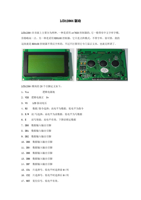
LCD12864驱动LCD12864在市面上主要分为两种,一种是采用st7920控制器的,它一般带有中文字库字模,价格略高一点。
另一种是采用KS0108控制器,它只是点阵模式,不带字库。
很可惜,我的这块就是KS0108控制器不带汉字库的,不过不打算用它专门显示文本,也就无所谓了。
LCD12864模块的20个引脚定义如下:1。
Vss 逻辑电源地2。
VDD 逻辑电源正5v3。
V0 LCD驱动电压4。
RS 数据/指令选择:高电平为数据,低电平为指令5。
R/W 读/写选择:高电平为读数据,低电平为写数据6。
E 读写使能,高电平有效,下降沿锁定数据7。
DB0 数据输入输出引脚8。
DB1 数据输入输出引脚9。
DB2 数据输入输出引脚10。
DB3 数据输入输出引脚11。
DB4 数据输入输出引脚12。
DB5 数据输入输出引脚13。
DB6 数据输入输出引脚14。
DB7 数据输入输出引脚15。
CS1 片选择号,低电平时选择前64列16。
CS2 片选择号,低电平时选择后64列17。
RET 复位信号,低电平有效。
18。
VEE 输出-15v电源给V0提供驱动电源19。
A 背光电源LED正极20。
K 背光电源LED负极具体电路图如下:制做如下:接口说明:装上12864具体的电路还是两个电阻。
一个背光限流电阻。
一个液晶驱动电压调节电阻。
背光电阻还是任何时候在19、20脚与电源之间串上个100欧电位器接上电源。
调节电位器到合适亮度。
具体值最好是到调试完程序能够正常显示后再将阻值确定换成固定电阻。
液晶驱动电压的调整在数据线、电源线接好的前提下是在Vee(-15v)和地之间接一个电位器。
中间接V0,通过调节电位器来调节V0上的电压。
当V0上为-15V时为全暗(液晶显示为全黑)。
当V0为0V 时为全亮。
调节电位器使屏幕从全暗刚好变到亮时,便可进行程序的调试。
待屏幕显示正常后,进行对比度的细调,然后测量这两边的阻值在地和V0之间、V0和Vee之间换成两个固定电阻焊上就好了。
#include <stdio.h>#include <math.h>#include <reg52.h>#include <string.h>/******************************************************************/ /* 定义数组*/ /******************************************************************/ unsigned char code IC_DAT[];unsigned char code pic1[];unsigned char code pic2[];unsigned char code pic3[];/******************************************************************/ /* 定义接口信息*/ /******************************************************************/ sbit RS =P2^4;sbit WRD=P2^5;sbit E= P2^6;sbit PSB=P2^1;sbit RES=P2^3;/******************************************************************/ /* 函数声明*/ /******************************************************************/void TransferData(char data1,bit DI);void display(void);void display_grapic(void);void delayms(unsigned int n);void DisplayLine(unsigned char line1,unsigned char line2);void DisplayGraphic(unsigned char code *adder);void delay(unsigned int m);void lcd_mesg(unsigned char code *adder1);unsigned char code IC_DAT[]={"上海浩豚电子科技""单片机开发板系列""中文字库测试程序""恭喜发财身体健康"};unsigned char code IC_DAT2[]={"海纳百川宽容为先""欲成大业诚信为先""游弋商海济世为先""人立于世守法为先"};/******************************************************************//* 液晶初始化-字库*//******************************************************************/void initinal(void) //LCD字库初始化程序{delay(40); //大于40MS的延时程序PSB=1; //设置为8BIT并口工作模式delay(1); //延时RES=0; //复位delay(1); //延时RES=1; //复位置高delay(10);TransferData(0x30,0); //Extended Function Set :8BIT设置,RE=0: basic instruction set, G=0 :graphic display OFFdelay(100); //大于100uS的延时程序TransferData(0x30,0); //Function Setdelay(37); ////大于37uS的延时程序TransferData(0x08,0); //Display on Controldelay(100); //大于100uS的延时程序TransferData(0x10,0); //Cursor Display Control光标设置delay(100); //大于100uS的延时程序TransferData(0x0C,0); //Display Control,D=1,显示开delay(100); //大于100uS的延时程序TransferData(0x01,0); //Display Cleardelay(10); //大于10mS的延时程序TransferData(0x06,0); //Enry Mode Set,光标从右向左加1位移动delay(100); //大于100uS的延时程序}/******************************************************************//* 液晶初始化-图形*//******************************************************************/void initina2(void) //LCD显示图片(扩展)初始化程序{delay(40); //大于40MS的延时程序PSB=1; //设置为8BIT并口工作模式delay(1); //延时RES=0; //复位delay(1); //延时RES=1; //复位置高delay(10);TransferData(0x36,0); //Extended Function Set RE=1: extended instructiondelay(100); //大于100uS的延时程序TransferData(0x36,0); //Extended Function Set:RE=1: extended instruction setdelay(37); ////大于37uS的延时程序TransferData(0x3E,0); //EXFUNCTION(DL=8BITS,RE=1,G=1)delay(100); //大于100uS的延时程序TransferData(0x01,0); //CLEAR SCREENdelay(100); //大于100uS的延时程序}/******************************************************************//* 主程序*//******************************************************************/void main(void){while(1){initina2(); //调用LCD显示图片(扩展)初始化程序DisplayGraphic(pic2); //显示图片2delayms(200);DisplayGraphic(pic3); //显示图片3delayms(200);initinal(); //调用LCD字库初始化程序delay(100); //大于100uS的延时程序lcd_mesg(IC_DAT); //显示中文汉字1delayms(240);delayms(240);initinal(); //调用LCD字库初始化程序delay(100); //大于100uS的延时程序lcd_mesg(IC_DAT2); //显示中文汉字2delayms(240);delayms(240);}}/******************************************************************/ /* 函数声明*/ /******************************************************************/void lcd_mesg(unsigned char code *adder1){unsigned char i;TransferData(0x80,0); //Set Graphic Display RAM Addressdelay(100);for(i=0;i<32;i++){TransferData(*adder1,1);adder1++;}TransferData(0x90,0); //Set Graphic Display RAM Addressdelay(100);for(i=32;i<64;i++){TransferData(*adder1,1);adder1++;}}/******************************************************************/ /* 函数声明*/ /******************************************************************/void TransferData(char data1,bit DI) //传送数据或者命令,当DI=0是,传送命令,当DI=1,传送数据.{WRD=0;RS=DI;delay(1);P0=data1;E=1;delay(1);E=0;}void delayms(unsigned int n) //延时10×n毫秒程序{unsigned int i,j;for(i=0;i<n;i++)for(j=0;j<2000;j++);}void delay(unsigned int m) //延时程序{unsigned int i,j;for(i=0;i<m;i++)for(j=0;j<10;j++);}/******************************************************************//* 函数声明*//******************************************************************/void DisplayGraphic(unsigned char code *adder){int i,j;//*******显示上半屏内容设置for(i=0;i<32;i++) //{TransferData((0x80 + i),0); //SET 垂直地址VERTICAL ADDTransferData(0x80,0); //SET 水平地址HORIZONTAL ADDfor(j=0;j<16;j++){TransferData(*adder,1);adder++;}}//*******显示下半屏内容设置for(i=0;i<32;i++) //{TransferData((0x80 + i),0); //SET 垂直地址VERTICAL ADDTransferData(0x88,0); //SET 水平地址HORIZONTAL ADDfor(j=0;j<16;j++){TransferData(*adder,1);adder++;}}}unsigned char code pic2[]={0xFF,0xFF,0xFF,0xFF,0xFF,0xFF,0xFF,0xFF,0xFF,0xFF,0xFF,0xFF,0xFF,0xFF,0xFF,0xFF,0xFF,0xFF,0xFF,0xFF,0xFF,0xFF,0xFF,0xFF,0xFF,0xFF,0xFF,0xFF,0xFF,0xFF,0xFF,0xFF,0xC0,0x00,0x00,0x00,0x00,0x00,0x00,0x00,0x00,0x00,0x00,0x00,0x00,0x00,0x00,0x03, 0xC0,0x00,0x00,0x00,0x00,0x00,0x00,0x00,0x00,0x00,0x00,0x00,0x00,0x00,0x00,0x03, 0xC0,0x00,0x00,0x00,0x00,0x00,0x00,0x00,0x00,0x00,0x00,0x00,0x00,0x00,0x00,0x03, 0xC0,0x00,0x00,0x00,0x00,0x00,0x00,0x00,0x00,0x00,0x00,0x00,0x00,0x00,0x00,0x03, 0xC0,0x00,0x00,0x00,0x00,0x00,0x00,0x00,0x00,0x00,0x00,0x00,0x00,0x00,0x00,0x03, 0xC0,0x00,0x00,0x00,0x00,0x00,0x00,0x00,0x00,0x00,0x00,0x00,0x00,0x00,0x00,0x03, 0xC0,0x1F,0xFF,0x81,0xFF,0xF0,0x00,0x00,0x00,0x00,0x00,0x00,0x00,0x00,0x00,0x03, 0xC0,0x1F,0xFF,0x81,0xFF,0xF0,0x00,0x00,0x00,0x00,0x00,0x00,0x00,0x00,0x00,0x03, 0xC0,0x18,0x01,0x80,0x00,0x00,0x00,0x00,0x00,0x00,0x20,0x08,0x00,0x00,0x00,0x03, 0xC0,0x1F,0xFF,0x80,0x00,0x00,0x04,0x07,0x81,0xE0,0x10,0x10,0x03,0xC0,0x30,0x03, 0xC0,0x1F,0xFF,0x80,0x00,0x00,0x0C,0x0C,0xC3,0x30,0x08,0x20,0x0C,0xE0,0x70,0x03, 0xC0,0x18,0x01,0x87,0xFF,0xFE,0x3C,0x18,0x66,0x18,0x04,0x40,0x0C,0x60,0x70,0x03, 0xC0,0x1F,0xFF,0x87,0xFF,0xFE,0x0C,0x18,0x66,0x18,0x02,0x80,0x18,0x00,0xB0,0x03, 0xC0,0x1F,0xFF,0x80,0x06,0x00,0x0C,0x18,0x66,0x18,0x01,0x00,0x1B,0x81,0x30,0x03, 0xC0,0x01,0x98,0x00,0x06,0x00,0x0C,0x00,0xE3,0x30,0x02,0x80,0x1C,0xC1,0x30,0x03, 0xC0,0x19,0x99,0x80,0x66,0x60,0x0C,0x00,0xC1,0xE0,0x04,0x40,0x18,0x62,0x30,0x03, 0xC0,0x19,0x99,0x80,0x66,0x30,0x0C,0x01,0x83,0x30,0x08,0x20,0x18,0x66,0x30,0x03, 0xC0,0x0D,0x9B,0x00,0xC6,0x38,0x0C,0x03,0x06,0x18,0x10,0x10,0x18,0x67,0xFC,0x03, 0xC0,0x0D,0x9B,0x01,0xC6,0x1C,0x0C,0x06,0x06,0x18,0x20,0x08,0x18,0x60,0x30,0x03, 0xC0,0x01,0x98,0x03,0x86,0x0C,0x0C,0x0C,0x06,0x18,0x00,0x00,0x08,0x60,0x30,0x03, 0xC0,0x7F,0xFF,0xE3,0x06,0x00,0x0C,0x18,0x03,0x30,0x00,0x00,0x0C,0xC0,0x30,0x03, 0xC0,0x7F,0xFF,0xE0,0x1E,0x00,0x0C,0x1F,0xE1,0xE0,0x00,0x00,0x07,0x80,0x30,0x03, 0xC0,0x00,0x00,0x00,0x1C,0x00,0x00,0x00,0x00,0x00,0x00,0x00,0x00,0x00,0x00,0x03, 0xC0,0x00,0x00,0x00,0x00,0x00,0x00,0x00,0x00,0x00,0x00,0x00,0x00,0x00,0x00,0x03, 0xC0,0x00,0x00,0x00,0x00,0x00,0x00,0x00,0x00,0x00,0x00,0x00,0x00,0x00,0x00,0x03, 0xC0,0x00,0x00,0x00,0x00,0x00,0x00,0x00,0x00,0x00,0x00,0x00,0x00,0x00,0x00,0x03,0xC0,0x00,0x00,0x00,0x00,0x00,0x00,0x00,0x00,0x00,0x00,0x00,0x00,0x00,0x00,0x03, 0xC0,0x00,0x00,0x00,0x00,0x00,0x00,0x00,0x00,0x00,0x00,0x00,0x00,0x00,0x00,0x03, 0xC0,0x00,0x00,0x00,0x00,0x00,0x00,0x00,0x00,0x00,0x00,0x00,0x00,0x00,0x00,0x03, 0xC0,0x00,0x00,0x00,0x00,0x00,0x0C,0x00,0x00,0x18,0x00,0x00,0x00,0x06,0x0C,0x03, 0xC3,0xFF,0xFC,0x3F,0xF0,0x80,0x0C,0x00,0x3F,0x18,0x01,0xFF,0xFE,0x06,0x0C,0x03, 0xC3,0xFF,0xFC,0x3F,0xF1,0x80,0x0F,0xFC,0x3F,0x18,0x01,0xFF,0xFE,0x06,0x0C,0x03,0xC3,0x0C,0x0C,0x0C,0xC3,0x00,0x0F,0xFC,0x33,0x7F,0xE1,0x86,0x06,0x06,0x0C,0x03, 0xC3,0x1F,0xCC,0x0C,0xC6,0x00,0x0C,0x00,0x33,0x7F,0xE1,0x8F,0xE6,0x06,0x0C,0x03, 0xC3,0x3F,0xCC,0x0C,0xCC,0x00,0x0C,0x00,0x36,0x30,0x01,0x9F,0xE6,0x07,0xFF,0xE3, 0xC3,0x79,0x8C,0x0C,0xC8,0x00,0xFF,0xF0,0x36,0x36,0x01,0xBC,0xC6,0x07,0xFF,0xE3, 0xC3,0x6F,0x0C,0x7F,0xF0,0xC0,0xFF,0xF0,0x36,0x66,0x01,0xB7,0x86,0x06,0x00,0x03, 0xC3,0x0F,0x0C,0x7F,0xF1,0x80,0xC0,0x30,0x36,0x7F,0xC1,0x87,0x86,0x06,0x00,0x03, 0xC3,0x79,0xEC,0x0C,0xC3,0x00,0xC0,0x30,0x33,0x7F,0xC1,0xBC,0xF6,0x06,0x00,0x03, 0xC3,0x76,0xEC,0x0C,0xC6,0x00,0xC0,0x30,0x33,0x06,0x01,0xBB,0x76,0x07,0xFF,0x03, 0xC3,0x07,0x0C,0x0C,0xCC,0x20,0xFF,0xF0,0x33,0x06,0x01,0x83,0x86,0x07,0xFF,0x03, 0xC3,0x03,0x0C,0x18,0xC8,0x60,0xFF,0xF0,0x3F,0x06,0x01,0x81,0x86,0x06,0x03,0x03, 0xC3,0x1C,0x0C,0x18,0xC0,0xC0,0x00,0x00,0x3E,0xFF,0xE1,0x8E,0x06,0x06,0x03,0x03, 0xC3,0x1F,0x0C,0x18,0xC1,0x81,0xB1,0x8C,0x30,0xFF,0xE1,0x8F,0x86,0x06,0x03,0x03, 0xC3,0x03,0x0C,0x30,0xC7,0x01,0xB1,0x8C,0x30,0x06,0x01,0x81,0x86,0x0C,0x03,0x03, 0xC3,0xFF,0xFC,0x70,0xDE,0x03,0x18,0xC6,0x30,0x06,0x01,0xFF,0xFE,0x0C,0x03,0x03, 0xC3,0xFF,0xFC,0x20,0x18,0x03,0x18,0xC6,0x30,0x06,0x01,0xFF,0xFE,0x18,0x03,0x03, 0xC0,0x00,0x00,0x00,0x00,0x00,0x00,0x00,0x00,0x00,0x00,0x00,0x00,0x00,0x00,0x03, 0xC0,0x00,0x00,0x00,0x00,0x00,0x00,0x00,0x00,0x00,0x00,0x00,0x00,0x00,0x00,0x03, 0xC0,0x00,0x00,0x00,0x00,0x00,0x00,0x00,0x00,0x00,0x00,0x00,0x00,0x00,0x00,0x03, 0xC0,0x00,0x00,0x00,0x00,0x00,0x00,0x00,0x00,0x00,0x00,0x00,0x00,0x00,0x00,0x03, 0xC0,0x00,0x00,0x00,0x00,0x00,0x00,0x00,0x00,0x00,0x00,0x00,0x00,0x00,0x00,0x03, 0xC0,0x00,0x00,0x00,0x00,0x00,0x00,0x00,0x00,0x00,0x00,0x00,0x00,0x00,0x00,0x03, 0xC0,0x00,0x00,0x00,0x00,0x00,0x00,0x00,0x00,0x00,0x00,0x00,0x00,0x00,0x00,0x03, 0xC0,0x00,0x00,0x00,0x00,0x00,0x00,0x00,0x00,0x00,0x00,0x00,0x00,0x00,0x00,0x03, 0xC0,0x00,0x00,0x00,0x00,0x00,0x00,0x00,0x00,0x00,0x00,0x00,0x00,0x00,0x00,0x03, 0xC0,0x00,0x00,0x00,0x00,0x00,0x00,0x00,0x00,0x00,0x00,0x00,0x00,0x00,0x00,0x03, 0xC0,0x00,0x00,0x00,0x00,0x00,0x00,0x00,0x00,0x00,0x00,0x00,0x00,0x00,0x00,0x03, 0xC0,0x00,0x00,0x00,0x00,0x00,0x00,0x00,0x00,0x00,0x00,0x00,0x00,0x00,0x00,0x03, 0xFF,0xFF,0xFF,0xFF,0xFF,0xFF,0xFF,0xFF,0xFF,0xFF,0xFF,0xFF,0xFF,0xFF,0xFF,0xFF,0xFF,0xFF,0xFF,0xFF,0xFF,0xFF,0xFF,0xFF,0xFF,0xFF,0xFF,0xFF,0xFF,0xFF,0xFF,0xFF,};unsigned char code pic3[]={0xFF,0xFF,0xFF,0xFF,0xFF,0xFF,0xFF,0xFF,0xFF,0xFF,0xFF,0xFF,0xFF,0xFF,0xFF,0xFF,0xFF,0xFF,0xFF,0xFF,0xFF,0xFF,0xFF,0xFF,0xFF,0xFF,0xFF,0xFF,0xFF,0xFF,0xFF,0xFF,0xC0,0x00,0x00,0x00,0x00,0x00,0x00,0x00,0x00,0x00,0x00,0x00,0x00,0x00,0x00,0x03, 0xC0,0x00,0x00,0x00,0x00,0x00,0x00,0x00,0x00,0x00,0x00,0x00,0x00,0x00,0x00,0x03,0xC0,0x00,0x00,0x00,0x00,0x00,0x00,0x00,0x00,0x00,0x00,0x00,0x00,0x00,0x00,0x03, 0xC0,0x00,0x00,0x00,0x00,0x00,0x00,0x00,0x00,0x00,0x00,0x00,0x00,0x00,0x00,0x03, 0xC3,0x02,0x0E,0x1C,0x08,0xF8,0x67,0xE3,0x87,0x0C,0x08,0x38,0x70,0x23,0xE1,0x83, 0xC4,0x8E,0x11,0x22,0x18,0x80,0x90,0x24,0x48,0x92,0x38,0x44,0x88,0x62,0x02,0x43, 0xC8,0x42,0x11,0x22,0x28,0x81,0x00,0x24,0x48,0xA1,0x08,0x44,0x88,0xA2,0x04,0x03, 0xC8,0x42,0x01,0x02,0x28,0xF1,0xE0,0x44,0x48,0xA1,0x08,0x04,0x08,0xA3,0xC7,0x83, 0xC8,0x42,0x02,0x0C,0x48,0x89,0x10,0x43,0x88,0xA1,0x08,0x08,0x31,0x22,0x24,0x43, 0xC8,0x42,0x04,0x02,0x88,0x09,0x10,0x44,0x47,0xA1,0x08,0x10,0x0A,0x20,0x24,0x43, 0xC8,0x42,0x08,0x22,0xFC,0x89,0x10,0x44,0x40,0xA1,0x08,0x20,0x8B,0xF2,0x24,0x43, 0xC4,0x82,0x10,0x22,0x08,0x89,0x10,0x84,0x49,0x12,0x08,0x40,0x88,0x22,0x24,0x43, 0xC3,0x02,0x1F,0x1C,0x08,0x70,0xE0,0x83,0x86,0x0C,0x08,0x7C,0x70,0x21,0xC3,0x83, 0xC0,0x00,0x00,0x00,0x00,0x00,0x00,0x00,0x00,0x00,0x00,0x00,0x00,0x00,0x00,0x03, 0xC0,0x00,0x00,0x00,0x00,0x00,0x00,0x00,0x00,0x00,0x00,0x00,0x00,0x00,0x00,0x03, 0xC0,0x00,0x00,0x00,0x00,0x00,0x00,0x00,0x00,0x00,0x00,0x00,0x00,0x00,0x00,0x03, 0xC0,0x00,0x00,0x00,0x00,0x00,0x00,0x00,0x00,0x00,0x00,0x00,0x00,0x00,0x00,0x03, 0xCF,0xC7,0x0E,0x18,0x10,0x70,0xE0,0x47,0xC3,0x3F,0x1C,0x38,0x60,0x41,0xC3,0x83, 0xC0,0x48,0x91,0x24,0x70,0x89,0x10,0xC4,0x04,0x81,0x22,0x44,0x91,0xC2,0x24,0x43, 0xC0,0x48,0x91,0x42,0x10,0x89,0x11,0x44,0x08,0x01,0x22,0x45,0x08,0x42,0x24,0x43, 0xC0,0x88,0x91,0x42,0x10,0x08,0x11,0x47,0x8F,0x02,0x22,0x45,0x08,0x40,0x20,0x43, 0xC0,0x87,0x11,0x42,0x10,0x10,0x62,0x44,0x48,0x82,0x1C,0x45,0x08,0x40,0x41,0x83, 0xC0,0x88,0x8F,0x42,0x10,0x20,0x14,0x40,0x48,0x82,0x22,0x3D,0x08,0x40,0x80,0x43, 0xC0,0x88,0x81,0x42,0x10,0x41,0x17,0xE4,0x48,0x82,0x22,0x05,0x08,0x41,0x04,0x43, 0xC1,0x08,0x92,0x24,0x10,0x81,0x10,0x44,0x48,0x84,0x22,0x48,0x90,0x42,0x04,0x43, 0xC1,0x07,0x0C,0x18,0x10,0xF8,0xE0,0x43,0x87,0x04,0x1C,0x30,0x60,0x43,0xE3,0x83, 0xC0,0x00,0x00,0x00,0x00,0x00,0x00,0x00,0x00,0x00,0x00,0x00,0x00,0x00,0x00,0x03, 0xC0,0x00,0x00,0x00,0x00,0x00,0x00,0x00,0x00,0x00,0x00,0x00,0x00,0x00,0x00,0x03, 0xC0,0x00,0x00,0x00,0x00,0x00,0x00,0x00,0x00,0x00,0x00,0x00,0x00,0x00,0x00,0x03, 0xC0,0x00,0x00,0x00,0x00,0x00,0x00,0x00,0x00,0x00,0x00,0x00,0x00,0x00,0x00,0x03, 0xC0,0x8F,0x86,0x7E,0x38,0x70,0xC0,0x83,0x87,0x02,0x3E,0x19,0xF8,0xE1,0xC3,0x03, 0xC1,0x88,0x09,0x02,0x44,0x89,0x23,0x84,0x48,0x86,0x20,0x24,0x09,0x12,0x24,0x83, 0xC2,0x88,0x10,0x02,0x44,0x8A,0x10,0x84,0x48,0x8A,0x20,0x40,0x09,0x12,0x28,0x43, 0xC2,0x8F,0x1E,0x04,0x44,0x8A,0x10,0x80,0x40,0x8A,0x3C,0x78,0x11,0x12,0x28,0x43, 0xC4,0x88,0x91,0x04,0x38,0x8A,0x10,0x80,0x83,0x12,0x22,0x44,0x10,0xE2,0x28,0x43, 0xC8,0x80,0x91,0x04,0x44,0x7A,0x10,0x81,0x00,0xA2,0x02,0x44,0x11,0x11,0xE8,0x43, 0xCF,0xC8,0x91,0x04,0x44,0x0A,0x10,0x82,0x08,0xBF,0x22,0x44,0x11,0x10,0x28,0x43, 0xC0,0x88,0x91,0x08,0x44,0x91,0x20,0x84,0x08,0x82,0x22,0x44,0x21,0x12,0x44,0x83, 0xC0,0x87,0x0E,0x08,0x38,0x60,0xC0,0x87,0xC7,0x02,0x1C,0x38,0x20,0xE1,0x83,0x03, 0xC0,0x00,0x00,0x00,0x00,0x00,0x00,0x00,0x00,0x00,0x00,0x00,0x00,0x00,0x00,0x03, 0xC0,0x00,0x00,0x00,0x00,0x00,0x00,0x00,0x00,0x00,0x00,0x00,0x00,0x00,0x00,0x03, 0xC0,0x00,0x00,0x00,0x00,0x00,0x00,0x00,0x00,0x00,0x00,0x00,0x00,0x00,0x00,0x03, 0xC0,0x00,0x00,0x00,0x00,0x00,0x00,0x00,0x00,0x00,0x00,0x00,0x00,0x00,0x00,0x03, 0xC1,0x07,0x0E,0x04,0x7C,0x33,0xF1,0xC3,0x86,0x04,0x1C,0x38,0x11,0xF0,0xCF,0xC3, 0xC7,0x08,0x91,0x0C,0x40,0x48,0x12,0x24,0x49,0x1C,0x22,0x44,0x31,0x01,0x20,0x43,0xC1,0x00,0x81,0x14,0x78,0xF0,0x22,0x24,0x50,0x84,0x02,0x04,0x51,0xE3,0xC0,0x83, 0xC1,0x01,0x06,0x24,0x44,0x88,0x21,0xC4,0x50,0x84,0x04,0x18,0x91,0x12,0x20,0x83, 0xC1,0x02,0x01,0x44,0x04,0x88,0x22,0x23,0xD0,0x84,0x08,0x05,0x10,0x12,0x20,0x83, 0xC1,0x04,0x11,0x7E,0x44,0x88,0x22,0x20,0x50,0x84,0x10,0x45,0xF9,0x12,0x20,0x83, 0xC1,0x08,0x11,0x04,0x44,0x88,0x42,0x24,0x89,0x04,0x20,0x44,0x11,0x12,0x21,0x03, 0xC1,0x0F,0x8E,0x04,0x38,0x70,0x41,0xC3,0x06,0x04,0x3E,0x38,0x10,0xE1,0xC1,0x03, 0xC0,0x00,0x00,0x00,0x00,0x00,0x00,0x00,0x00,0x00,0x00,0x00,0x00,0x00,0x00,0x03, 0xC0,0x00,0x00,0x00,0x00,0x00,0x00,0x00,0x00,0x00,0x00,0x00,0x00,0x00,0x00,0x03, 0xC0,0x00,0x00,0x00,0x00,0x00,0x00,0x00,0x00,0x00,0x00,0x00,0x00,0x00,0x00,0x03, 0xC0,0x00,0x00,0x00,0x00,0x00,0x00,0x00,0x00,0x00,0x00,0x00,0x00,0x00,0x00,0x03, 0xC0,0x00,0x00,0x00,0x00,0x00,0x00,0x00,0x00,0x00,0x00,0x00,0x00,0x00,0x00,0x03, 0xC0,0x00,0x00,0x00,0x00,0x00,0x00,0x00,0x00,0x00,0x00,0x00,0x00,0x00,0x00,0x03, 0xC0,0x00,0x00,0x00,0x00,0x00,0x00,0x00,0x00,0x00,0x00,0x00,0x00,0x00,0x00,0x03, 0xFF,0xFF,0xFF,0xFF,0xFF,0xFF,0xFF,0xFF,0xFF,0xFF,0xFF,0xFF,0xFF,0xFF,0xFF,0xFF,0xFF,0xFF,0xFF,0xFF,0xFF,0xFF,0xFF,0xFF,0xFF,0xFF,0xFF,0xFF,0xFF,0xFF,0xFF,0xFF,};。

12864](https://img.taocdn.com/s1/m/3b7b4f57f01dc281e53af0ac.png)
ST Sitronix ST7920Chinese Fonts built in LCD controller/driver Main Featuresz Voltage operating range:- 2.7 to 5.5Vz Support 8 bit, 4 bit, serial bus MPU interfacez64 x 16-bits character display RAM (max. 16 chars x 4 lines, LCD display range 16 char. X 2linesz64 x 256-bits graphic display RAM(GDRAM)z2M-bits Chinese fonts ROM (CGROM)supporting 8192 Chinese fonts (16x16 dotmatrix)z16K-bits half height ROM (HCGROM) supporting 126 character set (16x8 dot matrix)z64 x 16-bits character generation RAM (CGRAM)z15 x 16-bits total 240 ICON RAM(IRAM)z33-common x 64-segment (2 lines display) LCD driversz Automatic power on resetz External reset pin (XRESET)z With extension segment drivers display area can up to 16x2 lines z RC oscillator built in (with external R)z Low power designNormal mode (450uA Typ V DD=5V)Standby mode (30uA Max V DD=5V)z VLCD (V0~ V ss): max 7Vz Graphic and character mix modes display z Multiple instructions:- (Display clear)- (Return home)- (Display on/off)- (Cursor on/off)- (Display character blink)- (Cursor shift)- (Display shift)- (Vertical line scroll)- (By_line reverse display)- (Standby mode)z Built in voltage booster (2 times)z 1/33 DutyFunction DescriptionST7920 LCD controller/driver IC can display alphabets, numbers, Chinese fonts and self-defined characters. It supports 3 kinds of bus interface, namely 8 bit/ 4bit and serial. All functions, including display RAM, character generator ROM, LCD display drivers and control circuits are all in a one-chip solution. With a minimum system configuration, a Chinese character display system can easily achieved.ST7920 includes character ROM with 8192 16X16 dots Chinese fonts and 126 16X8 dots half height alphanumerical fonts. Also for graphic display it supports 64x256 dots graphic display area(GDRAM)and 240 dots ICON RAM. Mix mode display with both character and graphic data is possible. ST7920 has built in 4 sets CGRAM providing software programmable 16X16 font.ST7920 has wide operating voltage (2.7V to 5.5V) and low power consumption suitable for battery power portable device.ST7920 LCD driver consists of 33 common and 64 segments. Together with extension segment driver ST7921, ST7920 can support up to 33 common x 256 segments display.Product FonttypeST7920-0A BIG-5 code traditional character setST7920-0B GB code simplified character setST7920-0C GB code,BIG-5 code and Japanese codeST7920 Specification Revision HistoryVersion DateDescriptionC1.7 2000/12/151. VCC changed to VDD.2. VLCD changed from VCC-V5 to V0-VSS.3. DC characteristics input High voltage (Vih) changed to 0.7VDD.4. DC characteristics output High voltage (Voh) changed to 0.8VDD. C1.8 2001/03/011. Chip Size changed.2. ICON 256 dots changed to 240 dots.3. XOFF normal high sleep Low changed to normal low sleep High.4. Added XOFF application.5. Modified application of ST7920 4,5,6 PIN floating. (4,5,6為test pin)6. Modified voltage doubler CAP1P, CAP1M, CAP2M capacitors polarity C1.9 2001/05/28 1. Icon RAM TABLE changed. (TABLE-6) 2. Booster description modified. (PAGE-29)3. AC Characteristics modified.4. Added 2Line 16 Chinese Word (32Com X 256Seg) application circuit.5. Added oscillation resistor’s relation to power consumption and frequency.C2.0 2001/07/031. Added Register initial values.2. Voltage booster CAP1M CAP1P polarity changed. (PAGE-30)V2.0 2001/08/171. Modified Table 7. (PAGE-14)2. Change to English version.V2.0c 2001/10/18 1. Modified page-38 Serial interface timing diagramV2.0d 2002/05/091. Add the standard code (Japan 、GB code 、BIG-5 code) V3.02002/10/11 1. Delete sleep mode functionSystem Block diagramPads diagramorigin: center of chip coordinates: from pad centerchip size: 5305 X 4074 Pad open: 90 X 90Pad pitch: 125 unit: μm* chip substrate must connect to VSSPin coordinates unit: umNo. Name X Y1 V0 -2548 18122 V1 -2548 16883 V2 -2548 15624 N.C. -2548 14385 N.C. -2548 13126 N.C. -2548 11887 V3 -2548 10628 V4 -2548 9389 VSS -2548 81210 VDD -2548 68811 XRESET -2548 56212 CL1 -2548 43813 CL2 -2548 31214 VDD -2548 18815 M -2548 6216 DOUT -2548 -6217 RS -2548 -18818 RW -2548 -31219 E -2548 -43820 VSS -2548 -56221 OSC1 -2548 -68822 OSC2 -2548 -81223 PSB -2548 -93824 D0 -2548 -106225 D1 -2548 -118826 D2 -2548 -131227 D3 -2548 -143828 D4 -2548 -156229 D5 -2548 -168830 D6 -2548 -181231 D7 -2306 -193332 XOFF -2181 -193333 VOUT -2056 -193334 CAP3M -1931 -193335 CAP1P -1806 -193336 CAP1M -1681 -193337 CAP2P -1556 -193338 CAP2M -1431 -1933 X Y 39VD2 -1306 -1933 40C[1] -1181 -1933 41C[2] -1056 -1933 42C[3] -931 -1933 43C[4] -806 -1933 44C[5] -681 -1933 45C[6] -556 -1933 46C[7] -431 -1933 47C[8] -306 -1933 48C[9] -181 -1933 49C[10] -56 -1933 50C[11] 69 -1933 51C[12] 194 -1933 52C[13] 319 -1933 53C[14] 444 -1933 54C[15] 569 -1933 55C[16] 694 -1933 56C[17] 819 -1933 57C[18] 944 -1933 58C[19] 1069 -1933 59C[20] 1194 -1933 60C[21] 1319 -1933 61C[22] 1444 -1933 62C[23] 1569 -1933 63C[24] 1694 -1933 64C[25] 1819 -1933 65C[26] 1944 -1933 66C[27] 2069 -1933 67C[28] 2194 -1933 68C[29] 2319 -1933 69C[30] 2548 -1812 70C[31] 2548 -1688 71C[32] 2548 -1562 72C[33] 2548 -1438 73S[64] 2548 -1312 74S[63] 2548 -1188 75S[62] 2548 -1062 76S[61] 2548 -938No. Name X Y77 S[60] 2548 -81278 S[59] 2548 -68879 S[58] 2548 -56280 S[57] 2548 -43881 S[56] 2548 -31282 S[55] 2548 -18883 S[54] 2548 -6284 S[53] 2548 6285 S[52] 2548 18886 S[51] 2548 31287 S[50] 2548 43888 S[49] 2548 56289 S[48] 2548 68890 S[47] 2548 81291 S[46] 2548 93892 S[45] 2548 106293 S[44] 2548 118894 S[43] 2548 131295 S[42] 2548 143896 S[41] 2548 156297 S[40] 2548 168898 S[39] 2548 181299 S[38] 2319 1933 100 S[37] 2194 1933 101 S[36] 2069 1933 102 S[35] 1944 1933 103 S[34] 1819 1933 104 S[33] 1694 1933 105 S[32] 1569 1933 106 S[31] 1444 1933 107 S[30] 1319 1933 108 S[29] 1194 1933 109 S[28] 1069 1933 110 S[27] 944 1933 111 S[26] 819 1933 112 S[25] 694 1933 113 S[24] 569 1933 114 S[23] 444 1933 115 S[22] 319 1933 X Y 116S[21] 194 1933 117S[20] 69 1933 118S[19] -56 1933 119S[18] -181 1933 120S[17] -306 1933 121S[16] -431 1933 122S[15] -556 1933 123S[14] -681 1933 124S[13] -806 1933 125S[12] -931 1933 126S[11] -1056 1933 127S[10] -1181 1933 128S[9] -1306 1933 129S[8] -1431 1933 130S[7] -1556 1933 131S[6] -1681 1933 132S[5] -1806 1933 133S[4] -1931 1933 134S[3] -2056 1933 135S[2] -2181 1933 136S[1] -2306 1933Pin DescriptionName No. I/O Connects toFunctionXRESET 11I― System reset low active PSB 23 I―Interface selection:0: serial mode1: 8/4-bits parallel bus modeRS(CS*) 17 I MPURegister select0: select instruction write, busy flag read, address counter read1: select data write, read (Chip select) for serial mode 1: chip enable 0: chip disable RW(SID*) 18 I MPURead write control 0: write1: read(serial data input) E(SCLK*) 19 I MPUEnable trigger(serial clock)D4 to D7 28〜31I/O MPUHigher nibble data bus for 8 bit interface anddata bus for 4 bit interfaceD0 to D3 24〜27I/O MPU Lower nibble data bus for 8 bit interface CL1 12 O Extension segment tch signal for extension segment drivers CL2 13 O Extension segment drv.Shift clock for extension segment driversM 15 O Extension segment drv.AC signal for extension segment drivers voltageinversionDOUT16 O Extension segment drv.Data output for extension segment driversCOM1 to COM33 40〜72OLCDCommon signalsSEG1 to SEG64 136〜73O LCD Segment signalsV0 to V41〜37,8――LCD bias voltageV 0 -V4 ≦ 7 V V DD 10,14 I Power V DD : 2.7V to 5.5V Vss 9,20 IPower VSS: 0VOSC1, OSC2 21,22 I, O ResistorsFor internal oscillation resistor 5.0V R=33K2.7V R=18Kuse OSC1 for external clock inputVOUT33OResistors LCD voltage doubler output*note: The OSC pin must have the shortest wiring pattern of all other pins.To prevent noise from other signal lines , it should also beenclosed with the largest GND pattern possible. Poor noise characteristics on the OSC line will result in malfunction , or adversely affect the clock’s duty ratio.Pin descriptionNameNo. I/O Connects toDescriptionCAP3MCAP1PCAP1MCAP2M34 35 36 38I/O Capacitors Capacitor pins for voltage doublerXOFF 32 O― Reserved (no connection) CAP2P 37 ― ― Reserved (no connection)VD2 39 I Reference voltage Voltage doubler reference voltageN.C.N.C.N.C.4 5 6 I ― ― ― Test pins (no connection)Note:1. VDD>=V0>=V1>=V2>=V3>=V4 must be maintained2. Two clock options:3.When using voltage doubler for VOUT it is recommended that the total sum of bleeder resistors R1~R5 should be larger than 20K OhmR=33K (VDD=5.0V)R=18K (VDD=2.7V)Voltage doublerDoubler voltage mode VD2 & Vout output characteristic Notes:Follower loading resistor total 20k(ohm)Boostaer Cap use 4.7ufPanel size 80mm * 28mm (check display)Function Description :System interfaceST7920 supports 3 kinds of bus interface to MPU. 8 bits parallel, 4 bits parallel and clock synchronized serial interface. Parallel interface is selected by PSB=”1” and serial interface by PSB=”0”. 8 bit / 4 bit interface is selected by function set instruction DL bit.Two 8 bit registers (data register DR, instruction register IR) are used in ST7920’s write and read operation. Data Register(DR)can access DDRAM/CGRAM/GDRAM and IRAM’s data through the address pointer implemented by Address Counter (AC). Instruction Register (IR) stores the instruction by MPU to ST7920.4 modes of read/write operation specified by RS and RW:RS RW descriptionMPU write instruction to instruction register(IR)L LMPU read busy flag(BF)and address counter(AC)L HMPU write data to data register(DR)H LMPU read data from data register(DR)H HBusy Flag(BF)Internal operation is in progress when BF=”1”, ST7920 is in busy state. No new instruction will be accepted untilBF=”0”. MPU must check BF to determine whether the internal operation is finished and new instruction can be sent. Address counter(AC)Address counter(AC)is used for address pointer of DDRAM/CGRAM/IRAM/GDRAM. (AC) can be set by instruction and after data read or write to the memories (AC) will increase or decrease by 1 according to the setting in “entry mode set”. When RS=“0”and RW=“1”and E=”1” the value of(AC)will output to DB6〜DB0.16x16 character generation ROM (CGROM) and 8x16 half height ROM(HCGROM)ST7920 provides character generation ROM supporting 8192 16 x 16 character fonts and 126 8 x 16 alphanumeric characters. It is easy to support multi languages application such as Chinese and English. Two consecutive bytes are used to specify one 16x16 character or two 8x16 half-height characters. Character codes are written into DDRAM and the corresponding fonts are mapped from CGROM or HCGROM to the display drivers.Character generation RAM (CGRAM)ST7920 provides RAM to support user-defined fonts. Four sets of 16x16 bit map area are available. Theseuser-defined fonts are displayed the same ways as CGROM fonts through writing character cod data to DDRAM. ICON RAM(IRAM)ST7920 provides 240 ICON display. It consists of 15 sets of IRAM address. Each IRAM address has 16 bits data. IRAM address should be set first before writing to the IRAM. Two bytes for each address. First higher byte (D15~D8) and then lower byte (D7~D0).Table 4Display data RAM (DDRAM )There are 64x2 bytes for display data RAM area. Can store display data for 16 characters(16x16) by 4 lines or 32 characters(8x16) by 4 lines. However, only 2 lines can be displayed at a time. Character codes stored in DDRAM point to the fonts specified by CGROM ,HCGROM and CGRAM. ST7920 display half height HCGROM fonts, user-defined CGRAM fonts and full 16x16 CGROM fonts. Data codes 0000H 〜0006H are for CGRAMuser-defined fonts. Data codes 02H 〜7FH are for half height alpha numeric fonts. Data codes (A140〜D75F )are for BIG5 code and (A1A0〜F7FF) are for GB code.1. display HCGROM fonts :Write 2 bytes data to DDRAM to display two 8x16 fonts. Each byte represents 1 character font. The data of each byte is 02H 〜7FH.2. display CGRAM fonts :Write 2 bytes data to DDRAM to display one 16x16 font. Only 0000H ,0002H ,0004H , 0006H are allowed.3. display CGROM fonts :Write 2 bytes data to DDRAM to display one 16x16 font.A140H 〜D75FH are for (BIG5) code, A1A0H 〜F7FFH are for (GB) code.Higher byte (D15〜D8)are written first and then lower byte (D7〜D0). Refer to Table 5 for address mapCGRAM fonts and CGROM fonts can only be displayed in the start position of each address. (Refer toTable 4)8081 82 83 84 85 86 87 88 89 8A 8B 8C 8D 8E 8FH L H L H L H L H L H L H L H L H L H L H L H L H L H L H L H L S i t r o n i x S T 7 9 20 矽 創 電 子 .. 中 文 編 碼 (正 確) 矽創 電 子.. .中 文編碼Graphic RAM(GDRAM)Graphic display RAM supports 64x256 bits bit-mapped memory space. GDRAM address is set by writing 2 consecutive bytes for vertical address and horizontal address. Two-bytes data write to GDRAM for one address. Address counter will automatically increase by one for the next two-byte data. The procedure is as followings.1. Set vertical address(Y)for GDRAM2. Set horizontal address(X)for GDRAM3. Write D15〜D8 to GDRAM中(first byte)4. Write D7〜D0 to GDRAM中(second byte)Graphic display memory map please refer to Table-8LCD driverLCD driver have 33 common and 64 segments to drive the LCD panel. Segment data from CGRAM /CGROM /HCGROM are shifted into the 64 bits segment latches to display. Extended segment driver ST7921 can be used to extend the segment drivers to 256.DDRAM data (char. code) CGRAM Addr. CGRAM data (higher byte)CGRAM data (lower byte)B15~ B4 B 3 B 2 B 1 B 0 B 5B 4B 3B 2B 1B 0D 15D 14D 13D 12D 11D 10D 9D 8D 7D 6D 5D 4D 3D 2D 1 D0000000001000110000 0 000111111110010000000010000100000100010 0 0011000100000111111 0 0100001001001000010 0 0101001111001000010 0 0110011001010100100 0 0111101001100100100 010000010010001010000100100100100000100001010001001000010000 0 1011001111000010000 0 1100001001000100000011010000000010000000111000000001000000000 X 00 X 001111000000000000000 0 0000000011000000011 00001000110100000010 0 0010001000010011010 0 0011010111011010010 0 0100100000001010010 0 0101011111110010010 0 0110010000010010010 0 0111011111110010010 0 1000010000010010010 0 1001011111110010010 0 1010010000000010010 0 101101111111100010 0 1100101000001010010 0 1101101111111001110 0 1110101000001000100 0 0 X 01 X 011111000000000000000 0Table 5: DDRAM data (character code ), CGRAM data / address mapNote :1. DDRAM data (character code) bit1 and bit2 are the same as CGRAM address bit4 and bit5.2. CGRAM address bit0 to bit3 specify total 16 rows. Row16 is for cursor display. The data in row 16 will be logical OR to the cursor.3. CGRAM data for each address is 16 bits.4. DDRAM data to select CGRAM bit4 to bit15 must be “0”. Bit0 and bit3 value are “don’t care”.ICON RAM dataICON RAM addressSet SR ”0”, and then setHigher byte Lower byteIRAM address AC3….AC0AC3 AC2 AC1 AC0 D15 D14 D13 D12 D11D10D9D8D7D6D5D4 D3 D2 D1D0SEG4SEG5SEG6SEG7SEG8SEG9SEG10SEG11 SEG12 SEG13 SEG14SEG15SEG3SEG10 0 0 0 SEG0SEG20 0 0 1 SEG16 SEG17 SEG18 SEG19 SEG20SEG21SEG22SEG23SEG24SEG25SEG26SEG27 SEG28 SEG29 SEG30SEG31SEG35SEG34SEG36SEG37SEG38SEG39SEG40SEG41SEG42SEG43 SEG44 SEG45 SEG46SEG47 SEG320 0 1 0SEG330 0 1 1 SEG48 SEG49 SEG50 SEG51 SEG52SEG53SEG54SEG55SEG56SEG57SEG58SEG59 SEG60 SEG61 SEG62SEG63SEG66SEG67SEG68SEG69SEG70SEG71SEG72SEG73SEG74SEG75 SEG76 SEG77 SEG78SEG79SEG650 1 0 0SEG640 1 0 1 SEG80 SEG81 SEG82 SEG83 SEG84SEG85SEG86SEG87SEG88SEG89SEG90SEG91 SEG92 SEG93 SEG94SEG95SEG99SEG100SEG101SEG102SEG103SEG104SEG105SEG106SEG107 SEG108 SEG109 SEG110SEG111SEG98SEG970 1 1 0SEG960 1 1 1 SEG112 SEG113 SEG114 SEG115SEG116SEG117SEG118SEG119SEG120SEG121SEG122SEG123 SEG124 SEG125 SEG126SEG127SEG131SEG132SEG133SEG134SEG135SEG136SEG137SEG138SEG139 SEG140 SEG141 SEG142SEG143SEG130SEG1281 0 0 0SEG1291 0 0 1 SEG144 SEG145 SEG146 SEG147SEG148SEG149SEG150SEG151SEG152SEG153SEG154SEG155 SEG156 SEG157 SEG158SEG159SEG162SEG161SEG163SEG164SEG165SEG166SEG167SEG168SEG169SEG170SEG171 SEG172 SEG173 SEG174SEG1751 0 1 0SEG1601 0 1 1 SEG176 SEG177 SEG178 SEG179SEG180SEG181SEG182SEG183SEG184SEG185SEG186SEG187 SEG188 SEG189 SEG190SEG191SEG195SEG196SEG197SEG198SEG199SEG200SEG201SEG202SEG203 SEG204 SEG205 SEG206SEG207SEG1941 1 0 0SEG192SEG1931 1 0 1 SEG208 SEG209 SEG210 SEG211SEG212SEG213SEG214SEG215SEG216SEG217SEG218SEG219 SEG220 SEG221 SEG222SEG223SEG227SEG228SEG229SEG230SEG231SEG232SEG233SEG234SEG235 SEG236 SEG237 SEG238SEG2391 1 1 0SEG226SEG224SEG2251 1 1 1 --- --- --- --- --- --- --- --- --- --- --- --- --- --- --- ---Table 6 ICON RAM address, data and Segment pinsTable 7 16x8 half-height charactersTable 8 GDRAM display coordinates and corresponding addressInstructionsST7920 offers basic instruction set and extended instruction set: Instruction set 1: (RE=0: basic instruction)codeInsRS RW DB7 DB6 DB5 DB4 DB3 DB2 DB1 DB0Description Exec time(540KHZ)CLEAR 0 0 0 0 0 0 0 0 0 1Fill DDRAM with "20H", and set DDRAM address counter(AC)to "00H"1.6 msHOME 0 0 0 0 0 0 0 0 1 X Set DDRAM address counter(AC)to "00H", and put cursorto origin ;the content of DDRAM are not changed72usENTRY MODE 0 0 0 0 0 0 0 1 I/D SSet cursor position and display shift when doing write or readoperation72usDISPLAY ON/OFF 0 0 0 0 0 0 1 D C BD=1: display ONC=1: cursor ONB=1: blink ON72 usCURSORDISPLAY CONTROL 0 0 0 0 0 1 S/C R/L X XCursor position and display shift control ;the content ofDDRAM are not changed72 usFUNCTIONSET 0 0 0 0 1 DL XREX XDL=1 8-BIT interfaceDL=0 4-BIT interfaceRE=1: extended instructionRE=0: basic instruction72 usSETCGRAM ADDR. 0 0 0 1 AC5 AC4 AC3 AC2 AC1 AC0Set CGRAM address to address counter(AC)Make sure that in extended instruction SR=0 (scroll orRAM address select)72 usSETDDRAM ADDR. 0 0 1AC6AC5 AC4 AC3 AC2 AC1 AC0Set DDRAM address to address counter(AC)AC6 is fixed to 072 usREADBUSY FLAG(BF)& ADDR. 0 1 BF AC6 AC5 AC4 AC3 AC2 AC1 AC0Read busy flag(BF)for completion of internal operation, alsoRead out the value of address counter(AC)0 usWRITE RAM 1 0 D7 D6 D5 D4 D3 D2 D1 D0Write data to internal RAM(DDRAM/CGRAM/IRAM/GDRAM)72 usREAD RAM1 1 D7 D6 D5 D4 D3 D2 D1 D0Read data from internal RAM(DDRAM/CGRAM/IRAM/GDRAM)72 usInstruction set 2: (RE=1: extended instruction)codeInst.RS RW DB7 DB6 DB5 DB4 DB3 DB2 DB1 DB0description Exec. time(540KHZ)STANDBY 0 0 0 0 0 0 0 0 0 1Enter stand by mode, any other instruction can terminate(Com1..32 halted, only Com33 ICON can display)72 usSCROLL orRAM ADDR. SELECT 0 0 0 0 0 0 0 0 1 SRSR=1: enable vertical scroll positionSR=0: enable IRAM address (extended instruction)SR=0: enable CGRAM address(basic instruction)72 usREVERSE 0 0 0 0 0 0 0 1 R1 R0Select 1 out of 4 line ( in DDRAM) and decide whether toreverse the display by toggling this instructionR1,R0 initial value is 0072 usEXTENDEDFUNCTIONSET 0 0 0 0 1 DL X1REG 0DL=1 8-BIT interfaceDL=0 4-BIT interfaceRE=1: extended instruction setRE=0: basic instruction setG=1 :graphic display ONG=0 :graphic display OFF72 usSETIRAM or SCROLL ADDR 0 0 0 1 AC5 AC4 AC3 AC2 AC1 AC0SR=1: AC5~AC0 the address of vertical scrollSR=0: AC3~AC0 the address of ICON RAM72 usSETGRAPHIC RAM ADDR. 0 0 1AC6AC5AC4AC3AC3AC2AC2AC1AC1AC0AC0Set GDRAM address to address counter(AC)First set vertical address and the horizontal address byconsecutive writingVertical address range AC6...AC0Horizontal address range AC3…AC072 usNote:1.Make sure that ST7920 is not in busy state by reading the busy flag before sending instruction or data. If use delay loopinstead please make sure the delay time is enough. Please refer to the instruction execution time.2.“RE”is the selection bit of basic and extended instruction set. Each time when altering the value of RE it will remain.There is no need to set RE every time when using the same group of instruction set.Initial setting(Register flag) (RE=0: basic instruction)codeInst.RS RW DB7 DB6 DB5 DB4 DB3 DB2 DB1DB0Description0 0 0 0 0 0 0 1 I/D SENTRY MODE SET1 0Cursor move to right ,DDRAM address counter (AC )plus 10 0 0 0 0 0 1 D C BDISPLAY STATUS 0 0 0Display, cursor and blink ALL OFF0 0 0 0 0 1 S/C R/L X XCURSOR DISPLAY SHIFTX XNo cursor or display shift operation0 0 0 0 1 DL X0 REX XFUNCTIONSET1 08 BIT MPU interface , basic instruction setInitial setting(Register flag) (RE=1: extended instruction set)codeInst.RS RW DB7 DB6 DB5 DB4 DB3 DB2 DB1DB0description0 0 0 0 0 0 0 0 1 SRSCROLL ORRAM ADDR. SELECTAllow IRAMaddress or set CGRAM address0 0 0 0 0 0 0 1 R1 R0REVERSEBegin with normal and toggle to reverse0 0 0 0 1 DL X1REG 0EXTENDED FUNCTIONSETGraphic display OFFDescription of basic instruction setz CLEARFill DDRAM with "20H"(space code). And set DDRAM address counter (AC )to"00H". Set entry mode I/D bit to be "1". Cursor moves right and AC adds 1 after write or read operation. z HOMESet DDRAM address counter (AC )to "00H". Cursor moves to origin. Then content of DDRAM is not changed. z ENTRY MODE SETSet the cursor movement and display shift direction when doing write or read operation. I/D :address counter increase / decreaseWhen I/D = "1", cursor moves right, DRAM address counter (AC )add by 1. When I/D = "0", cursor moves left, DRAM address counter (AC )subtract by 1. S: Display shiftS I/D DESCRIPTIONH H Entire display shift left by 1 HLEntire display shift right by 10 0 0 0 0 0 0000000000000001CodeCodeCodeRSRSRSRW RW RW DB7DB7DB7DB6DB6DB6DB5DB5DB5DB4DB4DB4DB1DB1DB1DB2DB2DB2DB3DB3DB301I/D 1xSDB0DB0DB0zDISPLAY STATUSControls display, cursor and blink ON/OFF.D : Display ON/OFF control bit When D = "1", display ONWhen D = "0",display OFF , the content of DDRAM is not changed C : Cursor ON/OFF control bit When C = "1", cursor ON. When C = "0", cursor OFF. B : Blink ON/OFF control bitWhen B = "1", cursor position blink ON. Then display data in cursor position will blink. When B = "0", cursor position blink OFF z CURSOR AND DISPLAY SHIFT CONTROLInstruction to move the cursor or shift the entire display. The content of DDRAM is not changed.S/C R/L Description AC Value L L Cursor moves left by 1 AC=AC-1 L H Cursor moves right by 1AC=AC+1 H L Display shift left by 1, cursor also follows to shift. AC=AC HHDisplay shift right by 1, cursor also follows to shift.AC=AC0 0 0 0 00000011S/C D R/L CodeCodeRSRSRW RW DB7DB7DB6DB6DB5DB5DB4DB4DB1DB1DB2DB2DB3DB3C x BxDB0DB0ST7920V3.0 21/42 2002/10/11zFUNCTION SETDL : 4/8 BIT interface control bitWhen DL = "1", 8 BIT MPU bus interface When DL = "0", 為 4 BIT MPU bus interface RE : extended instruction set control bit When RE = "1", extended instruction set When RE = "0", basic instruction setIn same instruction cannot alter DL and RE at once. Make sure that change DL first then RE. zSET CGRAM ADDRESSSet CGRAM address to address counter (AC ) AC range is 00H..3FHMake sure that in extended instruction SR=0 (scroll address or RAM address select) z SET DDRAM ADDRESSSet DDRAM address to address counter (AC ). First line AC range is 80H..8FH Second line AC range is 90H..9FH Third line AC range is A0H..AFH Fourth line AC range is B0H..BFHPlease note that only 2 lines can be display at a time. zREAD BUSY FLAG (BF )AND ADDRESSRead busy flag (BF )can check whether internal operation is finished. At the same time the value of address counter0 0 001DL X RE CodeRSRW DB7DB6DB5DB4DB1DB2DB3x xDB00 00 1AC5AC4AC3AC2CodeRSRWDB7DB6DB5DB4DB1DB2DB3AC1AC0DB00 01 AC6 AC5AC4AC3AC2CodeRSRWDB7DB6DB5DB4DB1DB2DB3AC1AC0DB00 1BF AC6 AC5AC4AC3AC2CodeRSRW DB7DB6DB5DB4DB1DB2DB3AC1AC0DB0ST7920V3.0 22/42 2002/10/11(AC )is also read. When BF = “1” new instruction will not be accepted. Must wait for BF = “0” for new instruction.zWRITE DATA TO RAMWrite data to internal RAM and alter the (AC) by 1Each RAM address (CGRAM,DDRAM,IRAM…..) must write 2 consecutive bytes for 16 bit data. After the second byte the address counter will add or subtract by 1 according to the entry mode set control bit. z READ RAM DATARead data from internal RAM and alter the (AC) by 1After address set to read (CGRAM,DDRAM,IRAM…..)a DUMMY READ is required.There is no need to DUMMY READ for the following bytes unless a new address set instruction is issued.1 1 0 1 D7 D7 D6D6D5D5D4D4D3D3D2D2CodeCodeRSRSRW RW DB7DB7DB6DB6DB5DB5DB4DB4DB1DB1DB2DB2DB3DB3D1D1D0D0DB0DB0ST7920V3.0 23/42 2002/10/11Description of extended instruction setz STAND BYInstruction to enter stand by mode. Any other instruction follows this instruction can terminate stand by. The content of DDRAM remain the same. z VERTICAL SCROLL OR RAM ADDRESS SELECTWhen SR = "1", the vertical scroll address set is enabled.When SR = "0", the IRAM address set (extended instruction) and CGRAM address set (basic instruction) is enabled.z REVERSESelect 1 out of 4 lines to reverse the display and to toggle the reverse condition by repeating this instruction.R1,R0 initial vale is 00. When set the first time the display is reversed and set the second time the display become normal.R1 R0 Description L L First line normal or reverse L H Second line normal or reverse H L Third line normal or reverse HHFourth line normal or reversePlease note that only 2 lines out of 4 line display data can be displayed.0 0 0 0 0 0 0000000000000001CodeCodeCodeRSRSRSRW RW RW DB7DB7DB7DB6DB6DB6DB5DB5DB5DB4DB4DB4DB1DB1DB1DB2DB2DB2DB3DB3DB301R11SRR0DB0DB0DB0ST7920V3.0 24/42 2002/10/11z EXTENED FUNCTION SETDL : 4/8 BIT interface control bit When DL = "1", 8 BIT MPU interface When DL = "0", 4 BIT MPU interface RE : extended instruction set control bit When RE = "1", extended instruction set When RE = "0", basic instruction set G : Graphic display control bitWhen G = "1", graphic display ON When G = "0", Graphic display OFFIn same instruction cannot alter DL, RE and G at once. Make sure that change DL or G first and then RE. zSET IRAM OR SCROLL ADDRESSSR=1: AC5~AC0 is vertical scroll displacement address SR=0: AC3~AC0 is ICON RAM address z SET GRAPHIC RAM ADDRESSSet GDRAM address to address counter (AC ).First set vertical address and then horizontal address(write 2 consecutive bytes to complete vertical and horizontal address set) Vertical address range is AC6...AC0 Horizontal address range is AC3…AC0The address counter (AC )of graphic RAM(GRAM) only increment after write for horizontal address. After horizontal address =0FH it will automatically back to 00H. However, the vertical address will not increase as the result of the same action.0 0 001DL x RE CodeRSRW DB7DB6DB5DB4DB1DB2DB3G xDB01 AC6 AC5AC4AC3AC2CodeRSRWDB7DB6DB5DB4DB1DB2DB3AC1AC0DB00 00 1AC5AC4AC3AC2CodeRSRWDB7DB6DB5DB4DB1DB2DB3AC1AC0DB0。
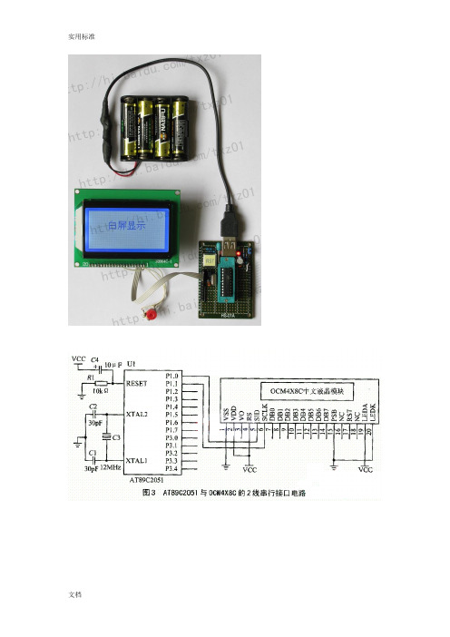
本例程为通过用A T89C52芯片操作LCD12864显示的程序,使用的晶振为12M。
/**********************************************************程序说明:LCD12864显示主程序程序调试员:莫剑辉调试时间:2010-6-7**********************************************************/#include<reg52.h>#include"12864.c"void main(){Ini_Lcd(); //液晶初始化子程序Disp(1,0,6,"莫剑辉"); //显示数据到LCD12864子程序while(1);}这里我们通过调用下面的头文件就可以了,这样的做法方便我们以后要用到LCD12864的程序的调用。
/**********************************************************程序说明:LCD12864显示头文件程序调试员:莫剑辉调试时间:2010-6-7**********************************************************///#include<reg52.h>#define uchar unsigned char#define uint unsigned int#define DATA P2 //数据输出端0~7sbit RS=P0^0; //LCD12864 RS端sbit RW=P0^1; //LCD12864 RW端sbit E =P0^2; //LCD12864 E 端sbit PSB =P0^3;/*********************************************延时子程序*********************************************/void Delay_1ms(uint x){uint j,i;for(j=0;j<x;j++){for(i=0;i<120;i++); //延时X乘以120}}/*********************************************LCD12864液晶测忙子程序(读状态)*********************************************/void Busy(){uchar busy;do{E = 0; //0为关闭使能端,1为打开使能端RS = 0; //1为指令,0为数据RW = 1; //1为读,0为写Delay_1ms(20); //延时20乘以120时间E = 1; //0为关闭使能端,1为打开使能端busy=P1; //读取P2状态Delay_1ms(20); //延时20乘以120时间E = 0; //0为关闭使能端,1为打开使能端}while(busy&0x80); //判断BUSY位是否工作:1为内部在工作,0为正常状态}/*********************************************LCD12864液晶数据写入子程序*********************************************/void Write_Data(uchar k){Busy(); //测忙E =1; //0为关闭使能端,1为打开使能端RS=1; //1为指令,0为数据RW=0; //1为读,0为写DA TA=k; //输入数据K到DA TADelay_1ms(20); //延时20乘以120时间E =0; //0为关闭使能端,1为打开使能端Delay_1ms(20); //延时20乘以120时间}/*********************************************LCD12864液晶命令写入子程序*********************************************/void Write_Cmd(uchar cmd){Busy(); //测忙E=1; //0为关闭使能端,1为打开使能端RS=0; //1为指令,0为数据RW=0; //1为读,0为写DA TA=cmd; //输入命令cmd到DATADelay_1ms(20); //延时20乘以120时间E=0; //0为关闭使能端,1为打开使能端Delay_1ms(20); //延时20乘以120时间}/*********************************************LCD12864液晶数据显示子程序*********************************************/void Disp(uchar y,uchar x,uchar i,uchar *z){uchar Address;if(y==1){Address=0x80+x;} //Y判断第几行,X判断第几列,0x80为液晶行初始地址if(y==2){Address=0x90+x;}if(y==3){Address=0x88+x;}if(y==4){Address=0x98+x;}Write_Cmd(Address); //写入地址命令到LCD12864while(i) //写入显示数据的大小{Write_Data(*(z++)); //写入显示数据到LCD12864i--;}}/*********************************************LCD12864液晶初始化子程序*********************************************/void Ini_Lcd(void){PSB=1;Delay_1ms(20);Write_Cmd(0x30); //基本指令集Delay_1ms(20);Write_Cmd(0x02); // 地址归位Delay_1ms(20);Write_Cmd(0x0c); //整体显示打开,游标关闭Delay_1ms(20);Write_Cmd(0x06); //游标右移Delay_1ms(20);Write_Cmd(0x80); //设定显示的起始地址Delay_1ms(20);Write_Cmd(0x01); //清除显示}。
lcd12864 程序流程图
我们常用的人机交互显示界面中,除了数码管,LED,以及我们之前已经提到的LCD1602 之外,还有一种液晶屏用的比较多。
相信接触过单片机的朋友都知道了,那就是12864 液晶。
顾名思义,12864 表示其横向可以显示128 个点,纵向可以显示64 个点。
我们常用的12864 液晶模块中有带字库的,也有不带字库的,其控制芯片也有很多种,如KS0108 、T6963,ST7920 等等。
在这里我们以ST7920 为主控芯片的12864 液晶屏来学习如何去驱动它。
(液晶屏采用金鹏的OCMJ4X8C)。
lcd12864 液晶说明:
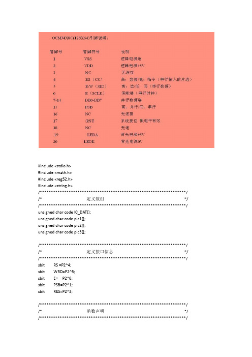
我们先来了解一下它的并行连接情况。
下面是电路连接图:
上面的图可以看出,液晶模块和单片机的连接除了P0 口的8 位并行数据线之外,还有RS,RW,E 等几根线。
其中R/S 是指令和数据寄存器的选择控制线(串行模式下为片选),R/W 是读写控制线(串行模式下是数据线),E 是使能线(串行模式下为时钟线)。
通过这几根控制线和数据线,再结合它的时序图,我们就可以编写出相应的驱动程序啦。
看看并行模式下的写时序图:。