TI锂电池均衡电路开发板电路图bq76PL536EVM-3
- 格式:pdf
- 大小:949.33 KB
- 文档页数:17

User's GuideSLUU437B–October2010–Revised May2011bq76PL536EVM Quick Start Guide1ScopeThis document covers the initial connection and installation of the Texas Instruments bq76PL536Evaluation Module(EVM),supplied in kit form including the EVM board,the Aardvark USB-SPI adapter, and connectors to make cells-to-EVM connection.It is not meant as a comprehensive guide to using the '536integrated circuit and its'features.See the device data sheet for details(SLUSA08).2Software Installation2.1PC Requirements1.Pentium1.66GHz(Core™2or better recommended)2.Windows-XP™SP2(software has not been tested with Windows Vista™/Win7)™2.0or later,with updates4.Available USB powered-port(hub OK if wall adapter used)2.2Installing the Aardvark DriverCAUTIONThe Aardvark driver must be installed before attaching the adapter for the firsttime.The Aardvark driver should be installed prior to installing the TI supplied bq76PL536Evaluation software.From the CD-ROM,run the file"/Tools/Aardvark/Drivers/TotalPhaseUSB-v2.xx.exe"to install the drivers.If prompted to do so,plug in the Aardvark to an available USB port using the supplied cable.The port must be a powered-port,typically directly from a e of a USB non-powered hub may not provide sufficient operating current for the Aardvark or EVM to operate correctly.2.3Installing the bq76PL536Evaluation SoftwareFrom the CD-ROM,run the file"/Software/bq76PL536Evaluation Software x_x_x.msi"to install,where the "x_x_x"is replaced by the current build number.Installation is automatic.This installs the GUI(Graphical User Interface)software for Windows.As new versions are released,they may be installed over theexisting version.Windows-XP,Windows Vista are trademarks of Microsoft Corporation.All other trademarks are the property of their respective owners.EVM Assembly and Configuration 3EVM Assembly and Configuration3.1Configure the Isolated Communications Interface3.1.15V vs3.3V SelectionIn the ISO-COMMS section of the PCB,there are two jumpers.JP5selects5V or3.3V I/O operationacross the isolation boundary.The Aardvark adapter supplied with the EVM uses3.3V logic,but is5Vtolerant.JP5should be configured for3.3V operation with the supplied Aardvark interface adapter,although either position will work correctly.For connection to a user supplied microcontroller,select the appropriate voltage.3.1.2Use USB Power from AardvarkJP1selects power from the USB connection through the Aardvark when installed in the“USB”position. 3.2Configure the EVM board3.2.1Use with CellsRemove jumpers JP1-18(18)located near the black battery connectors P1-P3to reduce the current draw of the board.It is OK to leave the jumpers in place;they connect a1K precision resistor between each adjacent pair of cell inputs and are supplied to use the EVM with power supplies in place of cells(see the Use with~12-26VDC Power Supply).Connect cells to the supplied mating connectors with screw terminals BEFORE plugging the connector into the EVM at P1,the large black connector on the left edge of the board.The most negative cellconnects to the most bottom of the black connector(P1).The bottom-most pin of the battery connector is the most negative connection to the board from thebattery stack.This is the negative end of cell1.The next pin up the connector is the positive end of cell1 (and the negative end of cell2).The connections proceed in this fashion up the connector to pin7,which is the most positive voltage from the battery stack connected to each IC.Pin7of P1(P1.7)is connected to P2.1on the board.The same is true of P2.7and P3.1.P3.7is connected to the top of the PCB(most positive voltage),while P1.1is connected to the bottom of the PCB(most negative voltage).The battery connections should be made secure,a loose connection may result in device destruction.Ideally,the cells are connected to one another by secure means such as welding,and only tap points are brought over to the EVM from each cell-to-cell interconnection.Although the device is immune to the effects of a random connection sequence,the ideal connectionsequence is from pin P1.1to pin3.7in order.TI recommends that users unfamiliar with the EVM and/or li-ion cells begin by using power supplies as outlined in the next section. EVM Assembly and Configuration 3.2.2Use with~12-26VDC Power SupplyImportant:Install jumpers JP1-18(18)located near the black battery connectors P1-P3before connecting power supplies.These jumpers connect a precision0.1%resistor divider network between cellconnections.Connect an appropriate power supply capable of supplying12-26VDC to connector P1,then plug P1into the EVM connector.Any voltage which meets the IC requirements will work,18-24V is typical of mostsix-cell systems.Plug additional supplies into P2and P3.The supplies must be isolated from each other and from earth ground to avoid unintentional short circuits.A separate supply is required for each IC (each cell-connection plug).The supply negative connection is made to pin1of the mating connector,the pin that will connect to the bottom-most pin of the mating connector.The positive connection is made to pin7,the top-most on the connector.It is not necessary to connect to the intermediate pins due to the resistive divider on the EVM which was enabled when JP1-18were installedCAUTIONDo not remove any of the jumpers JP1-18while using the EVM in thisconfiguration.Lethal DC voltages may be present for these configurations.Contact with these voltages may result in serious injury or eappropriate safety precautions.(+)and (–)outputsmust remain isolatedfrom earth ground.EVM Assembly and ConfigurationFigure 1.Correct Connection of Three ~20V Power Supplies to EVMFigure 2.Alternate Connection for Single 54V SupplyEVM Assembly and Configuration Figure 3.Incorrect Connections,Base IC Not PoweredFigure 4.Incorrect Connections,Insufficient V BAT Per ICFigure 5.Incorrect Connections,Top IC Not Powered,IC1,2Insufficient V BATConnecting the EVM 3.3Non-Critical Hardware Testing or Firmware Development3.3.1Stacking EVMsFor casual testing,one or two devices may be powered(in order from negative to positive)in lieu ofpowering all3devices.Due to poor termination of the unpowered devices in this configuration,detailed testing or critical hardware evaluations should not be undertaken.Any odd behavior or unexpected fault conditions should be ignored until verified with the EVM correctly powered by three isolated supplies4Connecting the EVM4.1Connection OrderFigure6.Bq76pl536EVM-3(a)Configure the EVM jumpers per Section3.1.(b)Connect the EVM to the Power Supplies or cells,turn on the supplies at~12to24V is recommended.The Absolute Maximum voltage per IC is36V and should not be exceeded,30V is the recommendedmaximum continuous voltage.(c)Connect the USB cable to the Aardvark and your PC.(d)Connect the Aardvark ribbon cable to the10pin header on the EVM boardThe Aardvark adapter should be connected last during power-up,and disconnected first whenpowering down.If not using the wall adapter to supply power,it must be after starting the Windowsapplication to avoid a turn-on issue with the Aardvark adapter.Many laptop computers power off theirUSB ports when they go into sleep,standby,or hibernate modes.If the device the Aardvark isconnected to remains powered when this happens,the Aardvark may suffer permanent damage.(e)Start the WinGUI User Interface software supplied with the EVM and installed earlier4.2Connection NotesThe ISO-COMMS section of the EVM board isolates the EVM side voltages completely from the PC side.It isolates all power,ground,and signal lines to the EVM.Caution must still be carefully taken when using the EVM as part of a stack,where lethal voltages may be present.The galvanic isolation provided by the ISO-COMMS section does not eliminate the need for safe handling procedures,proper High-Voltageequipment and protective clothing.Proper safety procedures should always be followed. Evaluation Software Details Because the ISO-COMMS circuit section fully isolates the PC,Aardvark,and wall adapter from the EVM “battery”side,the Aardvark is insensitive to the powering of the EVM,which receives its’power from the battery cells or power supply used for evaluation.The grounds(VSS)are fully isolated;please keep this in mind when using an oscilloscope or meter.Do not inadvertently connect the EVM VSS to the PC/Aardvark VSS by connecting two probe grounds orotherwise forming a ground loop through external wiring,including the building wiring.4.3Quick CheckThe first step in communicating with the bq76PL536is to set a unique address for each device in thestack.This is required even if you are only using a single device.This occurs automatically when theEvaluation software is first started.To do this manually,select COMMAND|AUTO ADDRESS(shortcut key CTRL+A).This will cause the software to interrogate the stack of‘536devices,find all availabledevices,and assign each a unique address beginning with address0x01.Address0x00is reserved for un-addressed devices.After addressing is complete,you should see the number of devices found and the total combined voltage of all cells being monitoring displayed in the STACK HEIGHT and V STACK windows.5Evaluation Software Details5.1Main ScreenThe main screen is divided into4major areas,plus the menu and status bars.The software is referred to as the“Windows Graphical User Interface”,or abbreviated to WinGUI.VBRIC K The voltage measured by the bq76PL536between the BATx and VSS pinsVCELLn the voltage measured between the pair of pins VCn–VCn-1(i.e.VCELL2=VC2-VC1).ADDR displays the address of the device being monitored in the measurement result area.LOG DEVICE Checking this box will add the contents of the device at this address to the log file.TSn The voltage measured between the TSn+and TSn-inputs,converted by the WinGUIto temperature based on the characteristics of the thermistor used in the EVM design.The EVM and WinGUI are configured to measure this voltage as a ratio of REG50,which removes any offset or gain errors introduced by drift in the REG50output.VIEW AS...Shows the ratio of the measured input voltage to REG50as a percentage.Evaluation Software Details Updates the displayed measurements for this device.The conversion is started bysending the register command CONVERT[CONV]=1,or hardware by toggling the CONV pin if the HW IO CONTROL box is checked.5.1.1Volatile RAM Configuration Registers–The lower half of this area displays the volatile configuration registers shown as bit fields,see thebq76PL536data sheet for details on programming these registers.These registers display green for logic 0,and orange for logic1.The two states may be toggled between by left-clicking on the bitThe STATUS,COV_FAULT,and CUV_FAULT bits are either white(logic0)or red(logic1)for asserted.In most cases,the asserted state indicates an error condition sensed by the bq76PL536.To clear a fault,first remove the physical condition causing the fault,then click on the ALERT or FAULT bit to reset the state of the bit.This writes a1to the bit,followed by a0,which is the device’s method for clearing the asserted bit state back to logic0.5.1.2Group-3Protected Registers–The device is provided with many configuration options set by bits contained in a special set of registers protected against accidental writing.These RAM registers are initialized from OTP(One-TimeProgrammable)EPROM cells.The device is shipped with these EPROM locations un-programmed(blank).The Windows GUI interface hides the un-programmed nature of the device by setting defaults in the registers cells when the Evaluation software starts(this can be defeated by setting the TOOLS|OPTIONS defaults).The last settings are also automatically saved by the GUI and restored on next use.These features are provided for ease of use,and are implemented solely in the ers areresponsible for programming OTP bits in parts correctly during manufacturing for correct operationin-circuit.Some Group-3registers are shown as registers at the bottom of the left side of the screen,the others in the top right section of the screen as listboxes and registers5.1.3Quick AccessThe Quick Access register(s)provide R/W access to any location in the part.They are named arbitrarily in the GUI‘X’,‘Y’,and‘Z’–there are no XYZ registers in the part.Some registers,such as the MASTER register require multi-byte writes to“unlock”the target register for writing.To accomplish this,program the X register address/data with the first unlock key,the Y register with the second unlock key,and finally the Z register with the target address and data.Then use the“write all”button to send all three address/data bytes in the correct order and timing to accomplish the multi-byte write.(This is done automatically when using the Protected Registers window.)5.1.4LED Status IndicatorsAt the top right of the user interface screen are8status indicator"LED's".These provide a quick view of the status of the devices,and the interface,cable connections,etc.Green normally indicates a logic0condition,and red a logic one condition.Gray indicates undefined. Evaluation Software Details ALERT A condition has been sensed that is causing the ALERT hardware pin to be asserted.This is also indicated by the ALERT bit being set(red)in the[DEVICE]STATUS register.Thesource of the ALERT condition is indicated in the ALERT register just below the STATUSregister.FAULT Similar to the ALERT indicator,this LED indicates the FAULT bit,and FAULT hardware pin are asserted.The source is indicated in the FAULT register,just below the ALERTregister.LAST CRC The last CRC received by the GUI was incorrect for the contents of the packet.Thisusually indicates a communications error caused by improper connection,excessivecabling,etc.The cause of the communications error should be corrected beforecontinuing.LOG Green if a log file is being written to.Logging is useful to capture information about cell or interface behavior over long periods of timeSTACK At least one device was found during auto-addressing or rebuild addresses.This indicates that the bottom device in the stack was found,is powered,not in POR,and the ribboncable from the Aardvark to the EVM is connected correctly.This verifies the cabling andconnection all the way to the IC.INTERFACE The Aardvark USB-SPI interface adapter was successfully found and communicated with.This verifies the cabling and driver to the adapter.5.1.5Global RegistersDEVICE The Address of the device currently being communicated with.Change to accessdifferent devices in the stack.“BROADCAST”mode also available to send a singlecommand to all devices in the stack.(In BROADCAST mode,no data is shown–theinterface can only display data from one device at a time.STACK HT.The number of devices found during the last AUTO-ADDRESS orREBUILD-ADDRESS cycle.POLL Check or un-check this box to turn polling on or off.Note that many menu items areunavailable during polling–turn polling off to access them.RATE This list box allows choosing a polling rate between100ms and60s.The LEDilluminates green each time the GUI polls the device eful as a heartbeatindicator when polling or logging is active.A setting“Fast”is also available.In thisposition,the WinGUI will poll as fast as possible,with only Windows OS slowing itdown.On most systems,this results in a poll every10-20ms,but your results may varydepending on the speed of your CPU and other tasks that are running.LOG STACK Enables or disables data logging.Logging is to a file in comma-separated-values(.csv) format.Set up logging in the LOG|SETUP menu.Logging may also be started/stopped under the LOG menu.Data is captured each poll,set by the polling interval inTOOLS|INTERFACE.VIEW PLOT Check this box to view a dynamic plot of data collected during polling.See PLOTTING for further information on configuring the plotter.Evaluation Software Details HW I/O Check this box to force the Evaluation software to use the hardware pins CONV andDRDY to initiate,and monitor ADC conversion cycles,instead of sending commands tothe CONVERT_CTRL[CONV]register bit.Similarly,it is monitoring the FAULT andALERT hardware pin states to determine a FAULT and/or ALERT condition beingpresent.Note that in HW I/O mode,the REFRESH button toggles the hardware CONVline,but the user may optionally use the CONVERT_CTRL[CONV]bit to force softwareinitiated conversions by clicking on the bit.5.2AddressingThe first step in communicating with thebq76PL536is to set a unique address for eachdevice in the stack.This is required even if you areonly using a single device.On the menu,selectCOMMAND|AUTO ADDRESS(shortcut key CTRL+A).This will cause the software to interrogate thestack of'536devices,find all available devices,andassign each a unique address beginning withaddress0x01.Address0x00is reserved forun-addressed devices.After addressing is complete,the number ofdevices found and the total combined voltage of allcells being monitoring are displayed in the STACKHEIGHT and V STACK windows.In this example,2bq76PL536devices are connected togethermonitoring12cells of about3.3V each.The screen automatically refreshes each time something changes.Addressing the device will cause all displayed values and registers to update.The user hould see all cell voltages displayed,along withregisters showing FAULT and ALERT status,DEVICE STATUS,etc.5.3Menus and Commands5.3.1File MenuThis menu provides a way to save complex registersettings between sessions.The settings are savedto a file on the local disk,selected using a dialogbox that appears when the Load or Save commandis selected.Multiple files,with different settings maybe saved under different file names.Saved registersettings are then re-loaded from the saved file.Allregisters–volatile and shadow–are saved orloaded,except the ADC measurementsAnother useful command available in this menu allows copying the current measurement data(VCn,VBRICK,and TS1,TS2,in that order)to the clipboard,and subsequent copying to a document orspreadsheet.measurements.It will also create Eprom programmable image for Bq76PL536OTP EPROM Programmer分销商库存信息: TIBQ76PL536EVM-3。
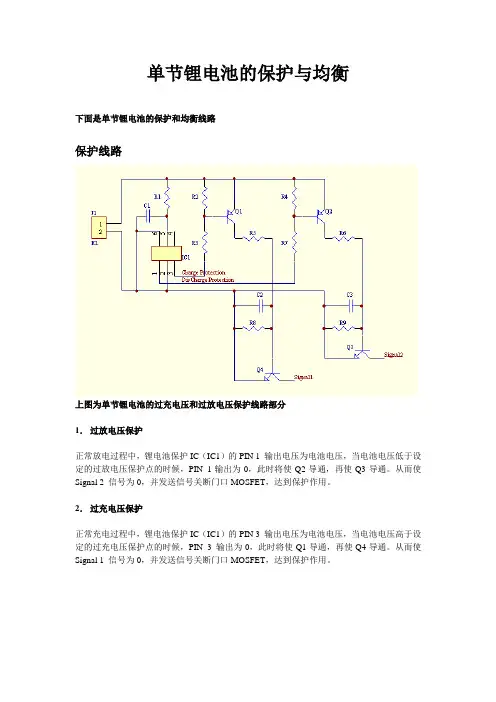
单节锂电池的保护与均衡
下面是单节锂电池的保护和均衡线路
保护线路
上图为单节锂电池的过充电压和过放电压保护线路部分
1.过放电压保护
正常放电过程中,锂电池保护IC(IC1)的PIN 1 输出电压为电池电压,当电池电压低于设定的过放电压保护点的时候,PIN 1输出为0,此时将使Q2导通,再使Q3导通。
从而使Signal 2 信号为0,并发送信号关断门口MOSFET,达到保护作用。
2.过充电压保护
正常充电过程中,锂电池保护IC(IC1)的PIN 3 输出电压为电池电压,当电池电压高于设定的过充电压保护点的时候,PIN 3 输出为0,此时将使Q1导通,再使Q4导通。
从而使Signal 1 信号为0,并发送信号关断门口MOSFET,达到保护作用。
均衡线路
上图为单节锂电池的均衡线路部分
均衡只有在充电过程中才会有。
(如想在放电过程中加入均衡,需加入CPU控制)
正常充电过程中,当电池电压到达设定的均衡电压点的时候,A点的电压将为2.5V,导致TL431导通。
TL431导通后,将使Q2、Q3(功率晶体管)导通。
当Q2导通后,由于有充电信号Signal 1 在,将有电压送进来,使B点电压抬升;而Q2导通前,由于B点电压被嵌死,故Signal 1 信号不会对此有影响。
B点电压抬升后,Q4导通,Signal 2 信号回送给充电器,要求关机,充电就会结束。
注:B点电压必须在每颗电池电压均达到均衡电压点的时候,才会被抬升,否则只要有一节电池还没开始均衡,B点电压就会始终被嵌死。

锂电池充电电路图2009-03-08 18:26锂电池是继镍镉、镍氢电池之后,可充电电池家族中的佼佼者.锂离子电池以其优良的特性,被广泛应用于: 手机、摄录像机、笔记本电脑、无绳电话、电动工具、遥控或电动玩具、照相机等便携式电子设备中。
一、锂电池与镍镉、镍氢可充电池:锂离子电池的负极为石墨晶体,正极通常为二氧化锂。
充电时锂离子由正极向负极运动而嵌入石墨层中。
放电时,锂离子从石墨晶体内负极表面脱离移向正极。
所以,在该电池充放电过程中锂总是以锂离子形态出现,而不是以金属锂的形态出现。
因而这种电池叫做锂离子电池,简称锂电池。
锂电池具有:体积小、容量大、重量轻、无污染、单节电压高、自放电率低、电池循环次数多等优点,但价格较贵。
镍镉电池因容量低,自放电严重,且对环境有污染,正逐步被淘汰。
镍氢电池具有较高的性能价格比,且不污染环境,但单体电压只有1.2V,因而在使用范围上受到限制。
二、锂电池的特点:1、具有更高的重量能量比、体积能量比;2、电压高,单节锂电池电压为3.6V,等于3只镍镉或镍氢充电电池的串联电压;3、自放电小可长时间存放,这是该电池最突出的优越性;4、无记忆效应。
锂电池不存在镍镉电池的所谓记忆效应,所以锂电池充电前无需放电;5、寿命长。
正常工作条件下,锂电池充/放电循环次数远大于500次;6、可以快速充电。
锂电池通常可以采用0.5~1倍容量的电流充电,使充电时间缩短至1~2小时;7、可以随意并联使用;8、由于电池中不含镉、铅、汞等重金属元素,对环境无污染,是当代最先进的绿色电池;9、成本高。
与其它可充电池相比,锂电池价格较贵。
三、锂电池的内部结构:锂电池通常有两种外型:圆柱型和长方型。
电池内部采用螺旋绕制结构,用一种非常精细而渗透性很强的聚乙烯薄膜隔离材料在正、负极间间隔而成。
正极包括由锂和二氧化钴组成的锂离子收集极及由铝薄膜组成的电流收集极。
负极由片状碳材料组成的锂离子收集极和铜薄膜组成的电流收集极组成。
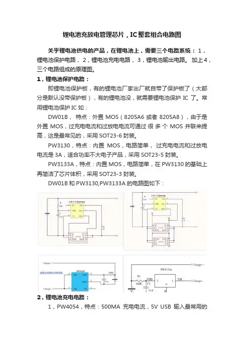
锂电池充放电管理芯片,IC整套组合电路图关乎锂电池供电的产品,在锂电池上,需要三个电路系统: 1,锂电池保护电路, 2,锂电池充电电路, 3,锂电池输出电路。
加上4,三个电路组成的原理图。
1,锂电池保护电路:即锂电池保护板,有的锂电池厂家出厂就自带了保护板了(大部分是默认没带保护板),有的锂电池没,就需要锂电池保护IC了。
常用锂电池保护IC如:DW01B,特点:外置MOS(8205A6或者8205A8),由于是外置MOS,过充电电流和过放电电流可通过很多个MOS并联来提高,这是最常见的,采用SOT23-6封装。
PW3130,特点:内置MOS,电路简单,过充电电流和过放电电流是3A,适合功率不大电子产品,采用SOT23-5封装。
PW3133A,特点:内置MOS,电路简单,在PW3130的基础上再简洁了芯片体积,采用SOT23-3封装。
DW01B和PW3130,PW3133A的电路图如下:2,锂电池充电电路:1,PW4054,特点:500MA充电电流,5V USB输入最常用的充电IC,采用SOT23-5封装;2,PW4056,特点:1A充电电流, 5V USB输入也是属于常用的充电IC,采用SOP8封装;3,PW4203,特点:5V,9V,12V,15V兼容高低压输入的锂电池充电IC,采用SOP8封装。
(注:产品很多,不能一一罗列,太多了,自行再添加)3,锂电池输出电路:1,锂电池自身供电电压是3V-4.2V之间,锂电池直接供电,电路就是直接接供电。
2,锂电池升压输出电路:PW5100,锂电池升压5V输出,输出电流在600MA,外围最简单;PW5300,锂电池升压4.5V~10V,输出功率6W(6W/电压=电流)PW5328B,锂电池升压4.5V ~20V。
(注:产品很多,不能一一罗列,太多了,自行再添加)3,锂电池降压输出电路:PW6566,LDO,输出3V,2.8V,2.5V,1.8V,1.5V,1.2V,电流最大250MA。
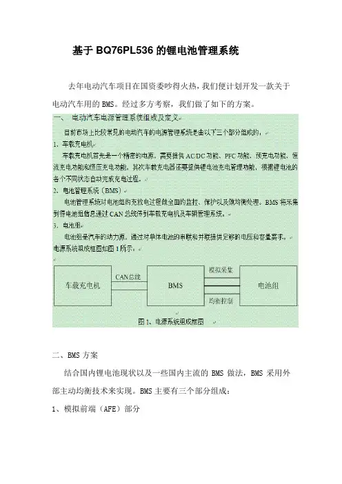
基于BQ76PL536的锂电池管理系统去年电动汽车项目在国资委吵得火热,我们便计划开发一款关于电动汽车用的BMS。
经过多方考察,我们做了如下的方案。
二、BMS方案结合国内锂电池现状以及一些国内主流的BMS做法,BMS采用外部主动均衡技术来实现。
BMS主要有三个部分组成:1、模拟前端(AFE)部分模拟前端主要实现电池组的串联,单组电池电压的采集,单组电池温度采集,单组电池过压欠压报警,主回路电流监控(包括放电和充电)。
2、主动均衡部分主动均衡部分主要通过超级电容对过压的单组电池进行电量泄放,对欠压的单组电池进行电量补充。
防止过充和过放对锂电池本身造成伤害,也避免了因发热造成的火花、燃烧甚至爆炸。
3、主控部分主控制器负责信号的收集与整理、均衡策略调整以、控制各个均衡电路工作、以及与充电机和汽车管理系统进行通信。
BMS系统框图如图2。
三、BMS具体实施1、模拟前端(AFE)部分AFE部分主要芯片使用TI的BQ76PL536A,主要负责单组电池电压的采集,单组电池温度采集,单组电池过压欠压报警。
BQ76PL536A 可以最多实现32组串联完全满足电动汽车需求。
BQ76PL536A利用差分输入方式,实现对单组电池进行电压采样并通过SPI总线将各个电池组的电压信息以及报警信息传送到主控单元,完成AFE的工作。
其具体电路如图3所示。
AFE另一部分用来实现主回路的电流采样,通过监测主回路的电流对电池组、充电机、汽车动力驱动电路进行保护。
当电流大小超过设定值主控单元通过CAN总线通知充电机和汽车管理系统进而可以切断电源对汽车电源系统起到保护作用。
采样电阻使用锰铜丝绕制,信号经过精密仪表用放大器(AD8230)隔离放大再到AD采集器(AD7170),AD采集器通过SPI总线将电流信息传输给主控单元。
或者用隔离放大器直接将信号传输到主控芯片,利用主控芯片集成的AD进行测量。
隔离放大器价格偏高,基本在20美金以上,所以暂不考虑。

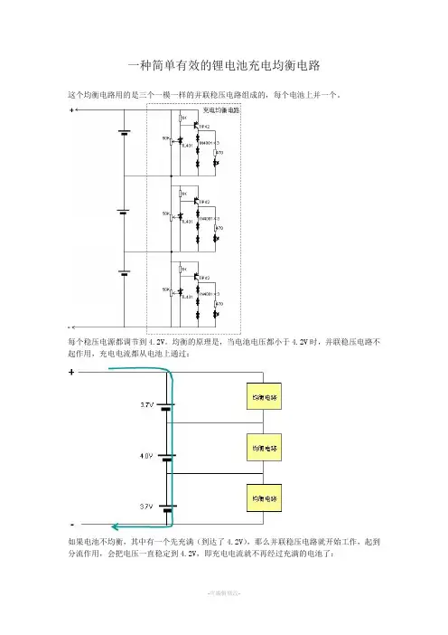
锂电池组均衡电路制作
锂电池组均衡电路是一种通过监测锂电池组中每个单体电池的电压,并根据电压差异自动调整电池充放电状态的电路。
以下是一些简单的制作锂电池组均衡电路的方法:
使用集成均衡器:可以使用市售的集成均衡电路芯片,例如ATtiny13A、BQ77PL157等,这些芯片具有自带保护和均衡功能,可以直接连接到锂电池组上。
DIY均衡器:可以通过购买均衡电路模块并通过串联连接来实现均衡功能。
在DIY设计时,需要根据实际的锂电池组情况(如电压、容量、数量等)选择合适的模块进行组装,通常还需要一定的电子基础知识和使用工具,因此需要谨慎操作。
自制均衡器:可以自己设计和制作均衡电路,电路板设计和焊接需要一定的电子技能。
首先需要确定所需的均衡器电路类型和参数,选择合适的元器件进行组装和连接,最后进行测试和验证。
在使用锂电池组均衡电路时,需要注意保证各单元电池的连接正确、均衡电路的稳定性和可靠性,以及保证锂电池组的安全使用。

均衡电路原理成组锂电池串联充电时,应保证每节电池均衡充电,否则使用过程中会影响整组电池的性能和寿命。
常用的均衡充电技术有恒定分流电阻均衡充电、通断分流电阻均衡充电、平均电池电压均衡充电、开关电容均衡充电、降压型变换器均衡充电、电感均衡充电等。
而现有的单节锂电池保护芯片均不含均衡充电控制功能;多节锂电池保护芯片均衡充电控制功能需要外接CPU,通过和保护芯片的串行通讯(如I2C总线)来实现,加大了保护电路的复杂程度和设计难度、降低了系统的效率和可靠性、增加了功耗。
本文针对动力锂电池成组使用,各节锂电池均要求充电过电压、放电欠电压、过流、短路的保护,充电过程中要实现整组电池均衡充电的问题,设计了采用单节锂电池保护芯片对任意串联数的成组锂电池进行保护的含均衡充电功能的电池组保护板。
锂电池组保护板均衡充电基本工作原理采用单节锂电池保护芯片设计的具备均衡充电能力的锂电池组保护板示意图如图1所示。
其中:1为单节锂离子电池;2为充电过电压分流放电支路电阻;3为分流放电支路控制用开关器件;4为过流检测保护电阻;5为省略的锂电池保护芯片及电路连接部分;6为单节锂电池保护芯片(一般包括充电控制引脚CO,放电控制引脚DO,放电过电流及短路检测引脚VM,电池正端VDD,电池负端VSS等);7为充电过电压保护信号经光耦隔离后形成并联关系驱动主电路中充电控制用MOS管栅极;8为放电欠电压、过流、短路保护信号经光耦隔离后形成串联关系驱动主电路中放电控制用MOS管栅极;9为充电控制开关器件;10为放电控制开关器件;11为控制电路;12为主电路;13为分流放电支路。
单节锂电池保护芯片数目依据锂电池组电池数目确定,串联使用,分别对所对应单节锂电池的充放电、过流、短路状态进行保护。
该系统在充电保护的同时,通过保护芯片控制分流放电支路开关器件的通断实现均衡充电。
图1 具备均衡充电能力的锂电池组保护板示意图当锂电池组充电时,外接电源正负极分别接电池组正负极BAT+和BAT-两端,充电电流流经电池组正极BAT+、电池组中单节锂电池1~N、放电控制开关器件、充电控制开关器件、电池组负极BAT-,电流流向如图2所示。


近年来,由于电池供电的便携式产品市场日益快速增长,锂离子 (Li-Ion) 电池的使用也随之变得普遍起来。
锂离子电池的一些卓越特性包括较高的重量及容积能量密度、低自放电率以及无记忆效应。
消费类电子产品世界将锂离子电池作为主要的便携式电源。
手机和笔记本电脑日益成为锂离子电池的主要用户。
随着锂离子电池的发展以及各种化学成份的日益普及,其他设备也可以利用锂离子的许多特性。
许多电动设备、电动汽车、医疗和工业设备现在也都使用锂离子电池作为其电源。
一些消费类应用要求单锂离子电池(如手机),或者需要三节串联和两节并联电池(如笔记本电脑)。
采用这种新设备,要求更高功率、更高容量以及更加稳健的电池组。
串联安装电池可以提高电压,而并联安装的电池则可以增加容量。
这些电池组数量不一,从笔记本电脑使用的六节电池到电动汽车中使用的数百节电池。
由于放大了锂离子电池的一些不足,这些要求给电池设计人员带来许多新的设计困难。
这些大容量电池要求先进的管理来确保获得高品质的设计。
我们必须考虑合适的温度、电压和电流测量。
随着锂离子电池组越来越大型,要求更多地关注散热管理、电池组可靠性、电池使用寿命和电池平衡。
实际上,随着电池组中所需电池数量的增加,电池单元之间的温度、容量和串联阻抗差异成为一个重要问题。
本文的大部分内容都将用于讨论这些差异带来的影响,以及如何在电池设计中控制这些差异。
电池的作用是为其主机存储和提供能量。
我们想尽可能多地向(从)电池组存储和获取能量。
妨碍多节电池组完成这一工作的主要方面是电池阻抗。
让我们来看一看其是如何影响向电池主机供电的。
在锂离子电池组中,存在一些允许每节串联电池达到的预定义电压最小值和最大值。
这是一种由电池组中 IC 控制的安全特性,请参见图 1A。
只要每一节电池均保持在过压和欠压断开范围之间,则该电池组便能够放电和充电。
如果一节电池达到上述任何一个阈值,则整个电池组便会关闭(欠压),从而让主机本应可用的电池组处于无法充电状态(请参见图 1B)。

新能源车辆电池管理系统设计与实现近年来,随着全球环保意识的不断提高和新能源技术的不断成熟,新能源车辆逐渐成为汽车市场中的热门产品。
但是,新能源车辆电池的管理系统同样至关重要。
本文将介绍新能源车辆电池管理系统的设计与实现。
一、新能源车辆电池管理系统的概述新能源车辆电池是车辆能量存储的关键部件,其管理系统包括电池状态监控、电池均衡、电池充电和放电管理等多个方面,是确保电池长期稳定运行的关键。
电池状态监控是电池管理系统的基础,可以实时监测电池的电压、电流、温度等参数,以确保电池正常工作。
同时,电池均衡管理可以实现电池之间的均衡,以保证各个电池单元的充电和放电一致。
电池充电和放电管理则是体现在车辆驾驶员的使用上,可以根据车辆的需求动态调节充电和放电以满足车辆运行的需要。
二、新能源车辆电池管理系统的设计1.硬件设计新能源车辆电池管理系统的硬件设计包括电池检测电路、均衡电路、电池充放电电路等。
其中,电池检测电路负责监测电池的电压、电流、温度等参数;均衡电路则根据电池状态实现电池之间的均衡;电池充放电电路则负责控制充电和放电的过程。
2.软件设计新能源车辆电池管理系统的软件设计包括控制算法和人机交互界面。
其中,控制算法是实现电池检测、均衡和充放电控制的核心部分;人机交互界面则可以显示电池运行状态、控制电池充放电以及设置电池充放电参数等。
三、新能源车辆电池管理系统的实现1.电池状态监测实现电池状态监测的实现需要选用高精度的电池检测器件,如TI公司的BQ76PL536A-Q1,可以实时监测电池的电压、电流、温度等参数,并提供具有可扩展性的实时数据监控传输接口。
2.电池均衡实现电池均衡实现需要选用高效的均衡电路,如TI公司的BQ76PL536A-Q1,可以将电池之间的差异均衡在1毫伏以下,从而保证各个电池单元的充电和放电一致。
3.充放电管理实现充放电管理实现需要选用高级的控制算法,如最大功率点跟踪控制,可以根据不同的电池状态确定最佳的充放电功率,从而保证电池长期稳定运行。
bq76PL536:电池管理集成电路
佚名
【期刊名称】《世界电子元器件》
【年(卷),期】2011(000)007
【摘要】德州仪器推出一款电池管理集成电路,其不但可延长充电锂离子电池组的使用寿命,而且还可较大限度提高混合动力电动车、电源工具以及不间断电源(UPS)应用的有效能量。
可堆栈bq76PL536电池监控器、平衡器与保护器整合模数转换器,支持独立电池电压及温度保护、电量平衡以及隔离芯片间的通信。
该器件可智能测量电池单元电压,支持1mV误差精度,可满足新型锂离子电池各种化学成分的需求。
【总页数】1页(P28-28)
【正文语种】中文
【中图分类】TN86
【相关文献】
1.美国国家半导体推出迷你型电池管理及保护集成电路 [J],
2.基于BQ76PL536的均衡系统设计 [J], 李峰; 张一鸣; 陈贺娜
3.动力电池管理系统的智能化技术——评《电动汽车智能电池管理系统技术》 [J], 张义
4.PS402:电池管理集成电路 [J],
5.bq2xxxx:TI的先进电池管理集成电路芯片组 [J],
因版权原因,仅展示原文概要,查看原文内容请购买。
锂离子电池组均衡系统张春强;冯能莲;王军;王小凤【摘要】为了提高锂离子电池组的可用容量,降低电池组中单体电池间容量不一致的影响,在专用电池管理芯片BQ76PL536A-Q1和单片机MSP430F5529的基础上,设计稳定运行的锂离子电池组均衡系统.利用模块化思想将锂离子电池组均衡系统分为采集板和核心板两大郝分.通过实时监测锂离子电池组的放电和均衡过程,对均衡系统的电压采集精度、电压监测和均衡功能进行验证.试验结果表明,锂离子电池组均衡系统能够降低电池组中容量不一致的程度,确保电池组稳定工作.【期刊名称】《山东交通学院学报》【年(卷),期】2016(024)002【总页数】6页(P94-99)【关键词】锂离子电池组;BQ76PL536A-Q1;均衡系统【作者】张春强;冯能莲;王军;王小凤【作者单位】安徽农业大学工学院,安徽合肥230036;安徽农业大学工学院,安徽合肥230036;安徽农业大学工学院,安徽合肥230036;安徽农业大学工学院,安徽合肥230036【正文语种】中文【中图分类】TM912为提高锂离子电池的输出功率,通常采用串联电池的方式来提高电压等级[1]。
由于各单体电池在生产过程中内阻、容量等参数不一致[2],并且电池组在使用过程中,各个单体电池会发生一些变化,电池的各参数也会不一致。
电池组内单元的不均衡将带来如下问题:1)电池组总容量得不到充分利用;2)容易造成电池单元的故障甚至损坏,形成安全隐患;3)需要增加更多的检测和控制电路[3-4]。
为了减小这种不一致性对锂离子电池组的影响,在电池组的充放电过程中需要增加均衡控制系统。
锂电池组均衡技术分为能耗型均衡和非能耗型均衡。
能耗型均衡主要为电阻放电式均衡,此种均衡结构简单,控制方便[5-6]。
由于非能耗型均衡的电路复杂,实现成本较高[7],故本系统采用能耗型均衡方案,采用电池管理专用集成芯片BQ76PL536A-Q1,完成串联锂离子电池均衡系统的设计,并进行试验论证。
分享⼏种锂电池均衡电路的⼯作原理原⽂新能源的发展,电动汽车发展,都会⽤到能量密度⽐更⾼的锂电池,⽽锂电池串联使⽤过程中,为了保证电池电压的⼀致性,必然会⽤到电压均衡电路。
在这⼏年的⼯作过程中,⽤到过⼏种电池的均衡电路,在这⾥就跟⼤家⼀起分享⼀下。
随着锂电池⽤途的增加,多节串联⼤容量锂电池的保护,电池管理及均衡必将会得到发展,希望⾃⼰做过的⼀些⼩东西能对⼤家有所帮助。
最简单的均衡电路就是负载消耗型均衡,也就是在每节电池上并联⼀个电阻,串联⼀个开关做控制,当某节电池电压过⾼时,打开开关,充电电流通过电阻分流,这样电压⾼的电池充电电流⼩,电压低的电池充电电流⼤,通过这种⽅式来实现电池电压的均衡,但这种⽅式只能适⽤于⼩容量电池,对于⼤容量电池来说是不现实的。
下图为⼀负载消耗性均衡的⽰意图第⼆种均衡⽅法我没有实验过,就是飞度电容法。
简单的说就是每⼀节电池并联⼀个电容,通过开关这个电容既可以并联到本⾝这节电池上,也可以并联到相邻的电池。
当某节电池电压过⾼,⾸先将电容与电池并联,电容电压与电池⼀致,然后将电容切换到相邻的电池,电容给电池放电。
实现能量的转移。
由于电容并不消耗能量,所以可以实现能量的⽆损转移。
但这种⽅式太繁琐了,现在的动⼒电池动不动⼏⼗节串联,要是采⽤这种⽅式,那的需要多少开关来控制啊。
下图为飞度电容法⼯作原理图,只是画出了相邻两节电池的均衡原理图。
第⼀次做均衡,是做的⼀款动⼒电池组的充电,电池容量80ah的两组并联,要求均衡电流为10a,原来了解的⼀点均衡的原理根本不够⽤啊,这么⼤电流都相当于⼀个⼀个的⼩模块了,最后还真的是搞了n个⼩模块串联,每节电池并联⼀个⼩模块,如果单体电池电压低于设定值,启动相应的并联模块,对低电压电池启动充电,补充能量提升电压,实现均衡。
下图为当时采⽤的均衡电路的⽰意图,DC-DC输⼊母线既可以是电池电压,也可是是别的模块提供的直流输⼊。
根据需要灵活配置。
主动均衡⽅法可以采⽤我前⾯提到的⼀个变压器多路输出的⽅法如果你想利⽤下⾯的电路⽰意图,做⼀个多路输出的反激电源,利⽤各个模块的输出电压来对电池实现均衡,我估计你需要很深的功⼒才可以,因为交叉调整率估计就会搞死你。
基于STM32F407+BQ76PL536的电池管理系统设计杨洁;廖俊杰;谷肖飞;路书祥;郑国恒【摘要】提出了一种基于STM32F407和BQ76PL536芯片的电池管理系统设计方案,实现了电池组中各个单体电池温度和电池电压的实时监测,以及在此基础上实现了以电池电压为均衡判据的充放电均衡处理策略,避免了电池充放电过程中的过温、过充、过放和充放电不均衡等现象,从而实现了延长电池使用寿命的目标.该方案设计有CAN总线接口,实现了电池管理主控板与其他设备的可靠通信,为电池管理系统的功能扩展提供了方便.【期刊名称】《电源技术》【年(卷),期】2018(042)011【总页数】4页(P1640-1643)【关键词】电池管理系统;电池均衡;BQ76PL536;STM32F407【作者】杨洁;廖俊杰;谷肖飞;路书祥;郑国恒【作者单位】郑州大学物理工程学院,河南郑州450001;郑州大学物理工程学院,河南郑州450001;郑州大学物理工程学院,河南郑州450001;郑州大学物理工程学院,河南郑州450001;郑州大学物理工程学院,河南郑州450001【正文语种】中文【中图分类】TM91能源和环境问题一直是当今汽车行业发展亟需解决的重要问题,因此节能环保的电动汽车成为汽车行业新的发展方向。
锂电池在所有类型的电池当中具有较高的能量密度和功率密度,因此成为当今电动汽车动力电池的首选。
电动汽车的动力电池大都是若干个单体锂电池串联组成一个电池组来使用,每一个电池组配备一套电源管理系统(BMS)。
因此,如何根据锂电池特性,设计相应的锂电池组电源管理系统,使得锂电池组能够高效地进行充放电管理,从而解决电池充放电过程中的过温、过充、过放和电池充放电不均衡等问题,对电动汽车锂电池组的安全使用以及延长电池组使用寿命有着重要的意义。
1 电池管理系统的组成本文提出的电池管理设计方案,是以STM32F407为核心控制器,以TI公司的BQ76PL536芯片为前端电源管理芯片的智能化电池管理系统。
基于 BQ78 PL116的锂离子电池组均衡电路
秦亮;李长录;毛辉
【期刊名称】《工业仪表与自动化装置》
【年(卷),期】2015(000)001
【摘要】针对锂离子电池由于单体电池电压较低通常串联使用,串联锂离子电池
组在多次充放电后产生的不均衡问题,提出一种基于BQ78PL116的PowerPump均衡电路。
该均衡电路使串联电池组中电压高的电池对电感进行充电,然后电感放电给电压低的电池,从而达到维持电池组均衡的目的。
通过对PowerPump电路的工作原理进行分析,说明此芯片具有结构简单,控制方便,
快速有效等优点。
该芯片应用在井下后备电源管理系统中,不仅能够延长电池寿命,更能提高管理系统的运行效率。
【总页数】4页(P42-45)
【作者】秦亮;李长录;毛辉
【作者单位】黑龙江科技大学电气工程学院,哈尔滨150022;中国煤炭科工集团
沈阳研究院,辽宁抚顺113000;黑龙江科技大学电气工程学院,哈尔滨150022【正文语种】中文
【中图分类】TM912.9
【相关文献】
1.基于UC3843的锂离子电池组均衡电路设计 [J], 陈晓飞;邹俊;沈军;张力
2.基于Boost-Buck电路的锂离子电池组均衡充电方法 [J], 陈益广;唐林;沈勇环
3.基于LC振荡电路的锂离子电池组主动均衡器 [J], 陆新秀;张鹏飞;祝令阵
4.基于Buck-Boost锂离子电池组均衡电路设计 [J], 李建辉;王彩申;林心笑
5.基于电感储能的新型锂离子电池组C2C均衡电路 [J], 林鸿业;康龙云;卢楚生;罗璇
因版权原因,仅展示原文概要,查看原文内容请购买。
一种基于MSP430F5529的锂电池组均衡方法及实现
张惠玲;周金治;郑希
【期刊名称】《电源技术》
【年(卷),期】2015(039)008
【摘要】锂电池组因单体电池之间的不一致,长期使用后将导致电池荷电状态出现差异,这种不均衡将使整个电池组效率降低.设计了一种基于SPI通信、以
MSP430F5529与Bq76PL536为核心的锂离子电池组均衡管理系统,通过电阻分流的均衡方式,实现单体电池之间的电压均衡,提高电池组的使用寿命和安全性能.【总页数】3页(P1652-1653,1696)
【作者】张惠玲;周金治;郑希
【作者单位】西南科技大学信息工程学院,四川绵阳621010;西南科技大学信息工程学院,四川绵阳621010;西南科技大学信息工程学院,四川绵阳621010
【正文语种】中文
【中图分类】TM912
【相关文献】
1.一种实现动力锂电池组充放电管理的主动均衡方察 [J], 刘小平;郭锋;刘宁一
2.基于双层准谐振开关电容的锂电池组均衡方法 [J], 李泉;周云山;王建德;傅兵
3.一种基于开关技术的锂电池组均衡方法及实现 [J], 简文宇;周金治;张惠玲
4.一种锂电池组动态调整型主动均衡方法研究与设计 [J], 夏斌
5.一种基于附加电池的锂电池组主动均衡方法 [J], 周萍;高寒;郑岳久;来鑫;周龙
因版权原因,仅展示原文概要,查看原文内容请购买。