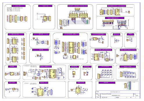
开发板电路原理图
- 格式:ppt
- 大小:74.50 KB
- 文档页数:9
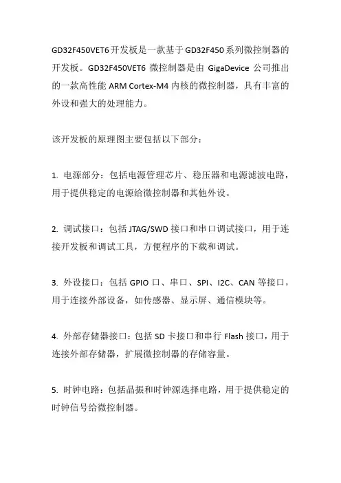
GD32F450VET6开发板是一款基于GD32F450系列微控制器的开发板。
GD32F450VET6微控制器是由GigaDevice公司推出的一款高性能ARM Cortex-M4内核的微控制器,具有丰富的外设和强大的处理能力。
该开发板的原理图主要包括以下部分:
1. 电源部分:包括电源管理芯片、稳压器和电源滤波电路,用于提供稳定的电源给微控制器和其他外设。
2. 调试接口:包括JTAG/SWD接口和串口调试接口,用于连接开发板和调试工具,方便程序的下载和调试。
3. 外设接口:包括GPIO口、串口、SPI、I2C、CAN等接口,用于连接外部设备,如传感器、显示屏、通信模块等。
4. 外部存储器接口:包括SD卡接口和串行Flash接口,用于连接外部存储器,扩展微控制器的存储容量。
5. 时钟电路:包括晶振和时钟源选择电路,用于提供稳定的时钟信号给微控制器。
6. 复位电路:包括复位按钮和复位电路,用于复位微控制器。
7. LED指示灯:用于显示系统状态。
8. 按键:用于用户输入。
9. 其他辅助电路:如电源开关、电源指示灯等。
通过这些原理图设计,GD32F450VET6开发板可以方便地进行嵌入式系统的开发和调试,支持各种外设的连接和扩展,满足不同应用场景的需求。
{"code":0,"msg":"请求出现异常","data":{}}。
SP601 Hardware User GuideUG518 (v1.7) September 26, 2012© Copyright 2009–2012 Xilinx, Inc. Xilinx, the Xilinx logo, Artix, ISE, Kintex, Spartan, Virtex, Zynq, and other designated brands included herein are trademarks of Xilinx in the United States and other countries. All other trademarks are the property of their respective owners. DISCLAIMERThe information disclosed to you hereunder (the “Materials”) is provided solely for the selection and use of Xilinx products. To the maximum extent permitted by applicable law: (1) Materials are made available “AS IS” and with all faults, Xilinx hereby DISCLAIMS ALL WARRANTIES AND CONDITIONS, EXPRESS, IMPLIED, OR ST ATUTORY, INCLUDING BUT NOT LIMITED TO WARRANTIES OF MERCHANTABILITY, NON-INFRINGEMENT, OR FITNESS FOR ANY PARTICULAR PURPOSE; and (2) Xilinx shall not be liable (whether in contract or tort, including negligence, or under any other theory of liability) for any loss or damage of any kind or nature related to, arising under, or in connection with, the Materials (including your use of the Materials), including for any direct, indirect, special, incidental, or consequential loss or damage (including loss of data, profits, goodwill, or any type of loss or damage suffered as a result of any action brought by a third party) even if such damage or loss was reasonably foreseeable or Xilinx had been advised of the possibility of the same. Xilinx assumes no obligation to correct any errors contained in the Materials, or to advise you of any corrections or update. Y ou may not reproduce, modify, distribute, or publicly display the Materials without prior written consent. Certain products are subject to the terms and conditions of the Limited Warranties which can be viewed at /warranty.htm; IP cores may be subject to warranty and support terms contained in a license issued to you by Xilinx. Xilinx products are not designed or intended to be fail-safe or for use in any application requiring fail-safe performance; you assume sole risk and liability for use of Xilinx products in Critical Applications:/warranty.htm#critapps.Revision HistoryThe following table shows the revision history for this document.Date Version Revision07/15/09 1.0Initial Xilinx release.08/19/09 1.1•Added Appendix B, VITA 57.1 FMC LPC Connector Pinout.•Updated Figure1-17.•Updated Table1-4, Table1-19, and Table1-22.•Added introductory paragraph to Appendix C, SP601 Master UCF.•Miscellaneous typographical edits and new user guide template.05/17/10 1.2•Updated Figure1-1, Figure1-2, Figure1-14, Figure1-18, Table1-9, Table1-1,Table1-11, and Table1-16.•Added Figure1-7, Figure1-8, and Table1-13.•Updated 9. VITA 57.1 FMC-LPC Connector, page25, Appendix B, VITA 57.1 FMCLPC Connector Pinout, and Appendix C, SP601 Master UCF.06/16/10 1.3Reversed order of 15. Configuration Options and 16. Power Management. Updated 1.Spartan-6 XC6SLX16-2CSG324 FPGA and 2. 128 MB DDR2 Component Memory. AddedTable1-26. Added UG394, Spartan-6 FPGA Power Management User Guide to Appendix D,References.09/24/10 1.4Added Power System Test Points, including Table1-25.02/16/11 1.5Added note and revised header description to indicate the I/Os support LVCMOS25signaling on page34. Revised oscillator manufacturer information from Epson to SiTimeon page page23 and page51.07/18/11 1.6Corrected wording from “PPM frequency jitter” to “PPM frequency stability” in sectionOscillator (Differential), page23. Added Table1-15, page27.09/26/12 1.7Added Regulatory and Compliance Information, page53.SP601 Hardware User Guide UG518 (v1.7) September 26, 2012SP601 Hardware User Guide 3UG518 (v1.7) September 26, 2012Revision History . . . . . . . . . . . . . . . . . . . . . . . . . . . . . . . . . . . . . . . . . . . . . . . . . . . . . . . . . . . . . 2Preface: About This GuideGuide Contents . . . . . . . . . . . . . . . . . . . . . . . . . . . . . . . . . . . . . . . . . . . . . . . . . . . . . . . . . . . . . . 5Additional Documentation . . . . . . . . . . . . . . . . . . . . . . . . . . . . . . . . . . . . . . . . . . . . . . . . . . . 5Additional Support Resources . . . . . . . . . . . . . . . . . . . . . . . . . . . . . . . . . . . . . . . . . . . . . . . . 6Chapter 1: SP601 Evaluation BoardOverview . . . . . . . . . . . . . . . . . . . . . . . . . . . . . . . . . . . . . . . . . . . . . . . . . . . . . . . . . . . . . . . . . . . . 7Additional Information. . . . . . . . . . . . . . . . . . . . . . . . . . . . . . . . . . . . . . . . . . . . . . . . . . . . . 7Features . . . . . . . . . . . . . . . . . . . . . . . . . . . . . . . . . . . . . . . . . . . . . . . . . . . . . . . . . . . . . . . . . . 8Block Diagram . . . . . . . . . . . . . . . . . . . . . . . . . . . . . . . . . . . . . . . . . . . . . . . . . . . . . . . . . . . . 9Related Xilinx Documents . . . . . . . . . . . . . . . . . . . . . . . . . . . . . . . . . . . . . . . . . . . . . . . . . . . . 9Detailed Description . . . . . . . . . . . . . . . . . . . . . . . . . . . . . . . . . . . . . . . . . . . . . . . . . . . . . . . . 101. Spartan-6 XC6SLX16-2CSG324 FPGA. . . . . . . . . . . . . . . . . . . . . . . . . . . . . . . . . . . . . . 11Configuration . . . . . . . . . . . . . . . . . . . . . . . . . . . . . . . . . . . . . . . . . . . . . . . . . . . . . . . . . 11I/O Voltage Rails . . . . . . . . . . . . . . . . . . . . . . . . . . . . . . . . . . . . . . . . . . . . . . . . . . . . . . 122. 128 MB DDR2 Component Memory . . . . . . . . . . . . . . . . . . . . . . . . . . . . . . . . . . . . . . . 123. SPI x4 Flash . . . . . . . . . . . . . . . . . . . . . . . . . . . . . . . . . . . . . . . . . . . . . . . . . . . . . . . . . . . . 154. Linear Flash BPI . . . . . . . . . . . . . . . . . . . . . . . . . . . . . . . . . . . . . . . . . . . . . . . . . . . . . . . . 175. 10/100/1000 Tri-Speed Ethernet PHY . . . . . . . . . . . . . . . . . . . . . . . . . . . . . . . . . . . . . 196. USB-to-UART Bridge. . . . . . . . . . . . . . . . . . . . . . . . . . . . . . . . . . . . . . . . . . . . . . . . . . . . 217. IIC Bus . . . . . . . . . . . . . . . . . . . . . . . . . . . . . . . . . . . . . . . . . . . . . . . . . . . . . . . . . . . . . . . . 228-Kb NV Memory . . . . . . . . . . . . . . . . . . . . . . . . . . . . . . . . . . . . . . . . . . . . . . . . . . . . . . 228. Clock Generation . . . . . . . . . . . . . . . . . . . . . . . . . . . . . . . . . . . . . . . . . . . . . . . . . . . . . . . 23Oscillator (Differential). . . . . . . . . . . . . . . . . . . . . . . . . . . . . . . . . . . . . . . . . . . . . . . . . . 23Oscillator Socket (Single-Ended, 2.5V or 3.3V) . . . . . . . . . . . . . . . . . . . . . . . . . . . . . . . . 24SMA Connectors (Differential). . . . . . . . . . . . . . . . . . . . . . . . . . . . . . . . . . . . . . . . . . . . 249. VITA 57.1 FMC-LPC Connector . . . . . . . . . . . . . . . . . . . . . . . . . . . . . . . . . . . . . . . . . . 2510. Status LEDs. . . . . . . . . . . . . . . . . . . . . . . . . . . . . . . . . . . . . . . . . . . . . . . . . . . . . . . . . . . 2811. FPGA Awake LED and Suspend Jumper. . . . . . . . . . . . . . . . . . . . . . . . . . . . . . . . . . 2912. FPGA INIT and DONE LEDs. . . . . . . . . . . . . . . . . . . . . . . . . . . . . . . . . . . . . . . . . . . . 3013. User I/O . . . . . . . . . . . . . . . . . . . . . . . . . . . . . . . . . . . . . . . . . . . . . . . . . . . . . . . . . . . . . 3114. FPGA_PROG_B Pushbutton Switch . . . . . . . . . . . . . . . . . . . . . . . . . . . . . . . . . . . . . . 3515. Configuration Options . . . . . . . . . . . . . . . . . . . . . . . . . . . . . . . . . . . . . . . . . . . . . . . . . 36JTAG Configuration . . . . . . . . . . . . . . . . . . . . . . . . . . . . . . . . . . . . . . . . . . . . . . . . . . . . 3616. Power Management. . . . . . . . . . . . . . . . . . . . . . . . . . . . . . . . . . . . . . . . . . . . . . . . . . . . 37AC Adapter and 5V Input Power Jack/Switch . . . . . . . . . . . . . . . . . . . . . . . . . . . . . . . . 37Onboard Power Supplies . . . . . . . . . . . . . . . . . . . . . . . . . . . . . . . . . . . . . . . . . . . . . . . . 37Power System Test Points . . . . . . . . . . . . . . . . . . . . . . . . . . . . . . . . . . . . . . . . . . . . . . . . 38Table of ContentsAppendix A: Default Jumper and Switch SettingsAppendix B: VITA 57.1 FMC LPC Connector PinoutAppendix C: SP601 Master UCFAppendix D: ReferencesAppendix E: Regulatory and Compliance InformationDirectives. . . . . . . . . . . . . . . . . . . . . . . . . . . . . . . . . . . . . . . . . . . . . . . . . . . . . . . . . . . . . . . . . . . 53Standards. . . . . . . . . . . . . . . . . . . . . . . . . . . . . . . . . . . . . . . . . . . . . . . . . . . . . . . . . . . . . . . . . . . 53 Electromagnetic Compatibility . . . . . . . . . . . . . . . . . . . . . . . . . . . . . . . . . . . . . . . . . . . . . 53Safety . . . . . . . . . . . . . . . . . . . . . . . . . . . . . . . . . . . . . . . . . . . . . . . . . . . . . . . . . . . . . . . . . . . 53 Markings . . . . . . . . . . . . . . . . . . . . . . . . . . . . . . . . . . . . . . . . . . . . . . . . . . . . . . . . . . . . . . . . . . . 54 SP601 Hardware User GuideUG518 (v1.7) September 26, 2012SP601 Hardware User Guide 5UG518 (v1.7) September 26, 2012PrefaceAbout This GuideThis manual accompanies the Spartan®-6 FPGA SP601 Evaluation Board and contains information about the SP601 hardware and software tools.Guide ContentsThis manual contains the following chapters:•Chapter 1, SP601 Evaluation Board , provides an overview of the SP601 evaluation board and details the components and features of the SP601 board.•Appendix A, Default Jumper and Switch Settings .•Appendix B, VITA 57.1 FMC LPC Connector Pinout .•Appendix C, SP601 Master UCF .•Appendix D, References .Additional DocumentationThe following documents are available for download at /products/spartan6.•Spartan-6 Family OverviewThis overview outlines the features and product selection of the Spartan-6 family.•Spartan-6 FPGA Data Sheet: DC and Switching CharacteristicsThis data sheet contains the DC and switching characteristic specifications for the Spartan-6 family.•Spartan-6 FPGA Packaging and Pinout SpecificationsThis specification includes the tables for device/package combinations and maximum I/Os, pin definitions, pinout tables, pinout diagrams, mechanical drawings, and thermal specifications.•Spartan-6 FPGA Configuration User GuideThis all-encompassing configuration guide includes chapters on configuration interfaces (serial and parallel), multi-bitstream management, bitstream encryption, boundary-scan and JTAG configuration, and reconfiguration techniques.•Spartan-6 FPGA SelectIO Resources User GuideThis guide describes the SelectIO™ resources available in all Spartan-6 devices.•Spartan-6 FPG A Clocking Resources User GuidePreface:About This GuideThis guide describes the clocking resources available in all Spartan-6 devices,including the DCMs and PLLs.•Spartan-6 FPGA Block RAM Resources User GuideThis guide describes the Spartan-6 device block RAM capabilities.•Spartan-6 FPGA DSP48A1 Slice User GuideThis guide describes the architecture of the DSP48A1 slice in Spartan-6FPGAs andprovides configuration examples.•Spartan-6 FPGA Memory Controller User GuideThis guide describes the Spartan-6 FPGA memory controller block, a dedicatedembedded multi-port memory controller that greatly simplifies interfacingSpartan-6FPGAs to the most popular memory standards.•Spartan-6 FPGA PCB Designer’s GuideThis guide provides information on PCB design for Spartan-6 devices, with a focus onstrategies for making design decisions at the PCB and interface level.Additional Support ResourcesTo search the database of silicon and software questions and answers or to create atechnical support case in WebCase, see the Xilinx website at:/support. SP601 Hardware User GuideUG518 (v1.7) September 26, 2012Chapter1 SP601 Evaluation BoardOverviewThe SP601 board enables hardware and software developers to create or evaluate designstargeting the Spartan®-6 XC6SLX16-2CSG324 FPGA.The SP601 provides board features for evaluating the Spartan-6 family that are common tomost entry-level development environments. Some commonly used features include aDDR2 memory controller, a parallel linear flash, a tri-mode Ethernet PHY, general-purposeI/O (GPIO), and a UART. Additional functionality can be added through the VITA 57.1.1expansion connector. Features, page8 provides a general listing of the board features withdetails provided in Detailed Description, page10.Additional InformationAdditional information and support material is located at:•/sp601This information includes:•Current version of this user guide in PDF format•Example design files for demonstration of Spartan-6 FPGA features and technology•Demonstration hardware and software configuration files for the SP601 linear and SPImemory devices•Reference Design Files•Schematics in PDF format and DxDesigner schematic format•Bill of materials (BOM)•Printed-circuit board (PCB) layout in Allegro PCB format•Gerber files for the PCB (Many free or shareware Gerber file viewers are available onthe internet for viewing and printing these files.)•Additional documentation, errata, frequently asked questions, and the latest newsFor information about the Spartan-6 family of FPGA devices, including product highlights,data sheets, user guides, and application notes, see the Spartan-6 FPGA website at/support/documentation/spartan-6.htm.SP601 Hardware User Guide 7 UG518 (v1.7) September 26, 2012Chapter 1:SP601 Evaluation BoardFeaturesThe SP601 board provides the following features (see Figure1-2 and Table1-1):• 1. Spartan-6 XC6SLX16-2CSG324 FPGA• 2. 128 MB DDR2 Component Memory• 3. SPI x4 Flash• 4. Linear Flash BPI• 5. 10/100/1000 Tri-Speed Ethernet PHY•7. IIC Bus•8Kb NV memory•External access 2-pin header•VITA 57.1 FMC-LPC connector•8. Clock Generation•Oscillator (Differential)•Oscillator Socket (Single-Ended, 2.5V or 3.3V)•SMA Connectors (Differential)•9. VITA 57.1 FMC-LPC Connector•10. Status LEDs•FPGA_AWAKE•INIT•DONE•13. User I/O•User LEDs•User DIP switch•User pushbuttons•GPIO male pin header•14. FPGA_PROG_B Pushbutton Switch•15. Configuration Options• 3. SPI x4 Flash (both onboard and off-board)• 4. Linear Flash BPI•JTAG Configuration•16. Power Management•AC Adapter and 5V Input Power Jack/Switch•Onboard Power Supplies SP601 Hardware User GuideUG518 (v1.7) September 26, 2012Related Xilinx DocumentsBlock DiagramFigure1-1 shows a high-level block diagram of the SP601 and its peripherals.Figure 1-1:SP601 Features and BankingRelated Xilinx DocumentsPrior to using the SP601 Evaluation Board, users should be familiar with Xilinx resources.See the following locations for additional documentation on Xilinx tools and solutions:•ISE: /ise•Answer Browser: /support•Intellectual Property: /ipcenterSP601 Hardware User Guide 9 UG518 (v1.7) September 26, 2012SP601 Hardware User GuideUG518 (v1.7) September 26, 2012Chapter 1:SP601 Evaluation BoardDetailed DescriptionFigure 1-2 shows a board photo with numbered features corresponding to Table 1-1 and the section headings in this document.The numbered features in Figure 1-2 correlate to the features and notes listed in Table 1-1.Figure 1-2:SP601 Board PhotoUG518_02_09100912843126137115109141581316Table 1-1:SP601 FeaturesNumberFeatureNotesSchematic Page1 Spartan-6 FP G A XC6SLX16-2CS G 3242DDR2 Component Elpida EDE1116ACBG 1Gb DDR2SDRAM53SPI x4 Flash and Headers SPI select and External Headers 84Linear Flash BPIStrataFlash 8-bit (J3 device), 3 pins shared w/ SPI x481. Spartan-6 XC6SLX16-2CSG 324 FPGAA Xilinx Spartan-6 XC6SLX16-2CSG324 FPGA is installed on the SP601 Evaluation Board.ReferencesSee the Spartan-6 FPGA Data Sheet . [Ref 1]ConfigurationThe SP601 supports configuration in the following modes:•Master SPI x4•Master SPI x4 with off-board device •BPI•JTAG (using the included USB-A to Mini-B cable)For details on configuring the FPGA, see 15. Configuration Options .The Mode DIP switch SW2 is set to M[1:0] = 01 Master SPI default.ReferencesSee the Spartan-6 FPGA Configuration User Guide for more information. [Ref 2]510/100/1000 Ethernet PHY GMII Marvell Alaska PHY76RS232 UART (USB Bridge)Uses CP2103 Serial-to-USB connection 107IICGoes to Header and VITA 57.1 FMC 108Clock, socket, SMA Differential, Single-Ended, Differential 99VITA 57.1 FMC-LPC connector LVDS signals, clocks, PRSNT 610LEDs Ethernet PHY Status711LED, Header FPGA Awake LED, Suspend Header 812LEDs FPGA INIT, DONE 913LED User I/O (active-High)9DIP SwitchUser I/O (active-High)9PushbuttonUser I/O, CPU_RESET (active-High)912-pin (8 I/O) Header6 pins x 2 male header with 8 I/Os (active-High)1014Pushbutton FPGA_PROG_B915USB JTAG Cypress USB to JTAG download cable logic14, 1516Onboard PowerPower Management11,12,13Table 1-1:SP601 Features (Cont’d)NumberFeatureNotesSchematic PageSP601 Hardware User Guide I/O Voltage RailsThere are four available banks on the LX16-CSG324 device. Banks 0, 1, and 2 are connected for 2.5V I/O. Bank 3 is used for the 1.8V DDR2 component memory interface of Spartan-6 FPGA’s hard memory controller. The voltage applied to the FPGA I/O banks used by the SP601 board is summarized in Table 1-2.ReferencesSee the Spartan-6 FPGA documentation for more information at /support/documentation/spartan-6.htm .2. 128 MB DDR2 Component MemoryThere are 128MB of DDR2 memory available on the SP601 board. A 1-Gb ElpidaEDE1116ACBG (84-ball) DDR2 memory component is accessible through Bank 3 of the LX16 device. The Spartan-6 FPGA hard memory controller is used for data transfer across the DDR2 memory interface’s 16-bit data path using SSTL18 signaling. The SP601 board supports the “standard” VCCINT setting of 1.20V ± 5%. This setting provides the standard memory controller block (MCB) performance of 625Mb/s for DDR2 memory in a -2 speed grade device. Signal integrity is maintained through DDR2 resistor terminations and memory on-die terminations (ODT), as shown in Table 1-3 and Table 1-4.Table 1-2:I/O Voltage Rail of FPGA BanksFPGA BankI/O Voltage Rail0 2.5V 1 2.5V 2 2.5V 31.8VTable 1-3:Termination Resistor RequirementsSignal NameBoard TerminationOn-Die TerminationDDR2_A[14:0]49.9Ω to V TT DDR2_BA[2:0]49.9Ω to V TT DDR2_RAS_N 49.9Ω to V TT DDR2_CAS_N 49.9Ω to V TT DDR2_WE_N 49.9Ω to V TT DDR2_CS_N 100Ω to GND DDR2_CKE 4.7K Ω to GND DDR2_ODT 4.7K Ω to GNDDDR2_DQ[15:0]ODT DDR2_UDQS[P ,N], DDR2_LDQS[P ,N]ODT DDR2_UDM, DDR2_LDMODTTable 1-5 shows the connections and pin numbers for the DDR2 Component Memory.DDR2_CK[P ,N]100Ω differential at memorycomponentNotes:1.Nominal value of V TT for DDR2 interface is 0.9V .Table 1-4:FPGA On-Chip (OCT) Termination External Resistor Requirements FPGA U1 PinFPGA Pin NumberBoard Connection for OCTZIO L6No Connect RZQC2100Ω to GROUNDTable 1-5:DDR2 Component Memory ConnectionsFPGA U1 PinSchematic Net Name Memory U2Pin NumberPin NameJ7DDR2_A0M8A0J6DDR2_A1M3A1H5DDR2_A2M7A2L7DDR2_A3N2A3F3DDR2_A4N8A4H4DDR2_A5N3A5H3DDR2_A6N7A6H6DDR2_A7P2A7D2DDR2_A8P8A8D1DDR2_A9P3A9F4DDR2_A10M2A10D3DDR2_A11P7A11G6DDR2_A12R2A12L2DDR2_DQ0G8DQ0L1DDR2_DQ1G2DQ1K2DDR2_DQ2H7DQ2K1DDR2_DQ3H3DQ3H2DDR2_DQ4H1DQ4H1DDR2_DQ5H9DQ5J3DDR2_DQ6F1DQ6Table 1-3:Termination Resistor Requirements (Cont’d)Signal NameBoard Termination On-Die TerminationSP601 Hardware User Guide ReferencesSee the Elpida DDR2 SDRAM Specifications for more information. [Ref 11]Also, see the Spartan-6 FPGA Memory Controller User Guide . [Ref 3]J1DDR2_DQ7F9DQ7M3DDR2_DQ8C8DQ8M1DDR2_DQ9C2DQ9N2DDR2_DQ10D7DQ10N1DDR2_DQ11D3DQ11T2DDR2_DQ12D1DQ12T1DDR2_DQ13D9DQ13U2DDR2_DQ14B1DQ14U1DDR2_DQ15B9DQ15F2DDR2_BA0L2BA0F1DDR2_BA1L3BA1E1DDR2_BA2L1BA2E3DDR2_WE_B K3WE L5DDR2_RAS_B K7RAS K5DDR2_CAS_B L7CAS K6DDR2_ODT K9ODT G3DDR2_CLK_P J8CK G1DDR2_CLK_N K8CK H7DDR2_CKE K2CKE L4DDR2_LDQS_P F7LDQS L3DDR2_LDQS_N E8LDQS P2DDR2_UDQS_P B7UDQS P1DDR2_UDQS_N A8UDQS K3DDR2_LDM F3LDM K4DDR2_UDMB3UDMTable 1-5:DDR2 Component Memory Connections (Cont’d)FPGA U1 PinSchematic Net Name Memory U2Pin NumberPin Name3. SPI x4 FlashThe Xilinx Spartan-6 FPGA hosts a SPI interface which is accessible to the Xilinx iMPACTconfiguration tool. The SPI memory device operates at 3.0V; the Spartan-6 FPGA I/Os are3.3V tolerant and provide electrically compatible logic levels to directly access the SPI flashthrough a 2.5V bank. The XC6SLX16-2CSG324 is a master device when accessing anexternal SPI flash memory device.The SP601 SPI interface has two parallel connected configuration options (see Figure1-4):an SPI X4 (Winbond W25Q64VSFIG) 64-Mb flash memory device and a flashprogramming header (J12). J12 supports a user-defined SPI mezzanine board. The SPIconfiguration source is selected via SPI select jumper J15. For details on configuring theFPGA, see 15. Configuration Options.Figure 1-3:J12 SPI Flash Programming HeaderSP601 Hardware User Guide ReferencesSee the Winbond Serial Flash Memory Data Sheet for more information. [Ref 12]See the XPS Serial Peripheral Interface Data Sheet for more information. [Ref 4]Figure 1-4:SPI Flash Interface TopologyTable 1-6:SPI x4 Memory ConnectionsFPGA U1 PinSchematic Net Name SPI MEM U17SPI HDR J12Pin #Pin NamePinNumberPin NameV2FPGA_PROG_B 1V14FPGA_D2_MISO31IO3_HOLD_B 2T14FPGA_D1_MISO2_R 9IO2_WP_B3V3SPI_CS_B4TMS T13FPGA_MOSI_CSI_B_MISO015DIN 5TDI R13FPGA_D0_DIN_MISO_MISO18IO1_DOUT6TDO R15FPGA_CCLK16CLK7TCK 8GND 9VCC3V3J15.2SPIX4_CS_B 7CS_B4. Linear Flash BPIAn 8-bit (16MB) Numonyx linear flash memory (TE28F128J3D-75) (J3D type) is used toprovide non-volatile bitstream, code, and data storage. The J3D devices operate at 3.0V; theSpartan-6 FPGA I/Os are 3.3V tolerant and provide electrically compatible logic levels todirectly access the linear flash BPI through a 2.5V bank. For details on configuring theFPGA, see 15. Configuration Options.Figure 1-5:Linear Flash BPI InterfaceTable 1-7:BPI Memory ConnectionsFPGA U1 Pin Schematic Net Name BPI Memory U10Pin Number Pin Name K18FLASH_A032A0K17FLASH_A128A1J18FLASH_A227A2J16FLASH_A326A3G18FLASH_A425A4G16FLASH_A524A5H16FLASH_A623A6H15FLASH_A722A7H14FLASH_A820A8H13FLASH_A919A9F18FLASH_A1018A10F17FLASH_A1117A11K13FLASH_A1213A12K12FLASH_A1312A13E18FLASH_A1411A14E16FLASH_A1510A15G13FLASH_A168A16SP601 Hardware User Guide Note:Memory U10 pin 56 address A24 is not connected on the 16 MB device. It is made availablefor larger density devices.ReferencesSee the Numonyx Embedded Flash Memory Data Sheet for more information. [Ref 13]In addition, see the Spartan-6 FPGA Configuration User Guide for more information. [Ref 2]H12FLASH_A177A17D18FLASH_A186A18D17FLASH_A195A19G14FLASH_A204A20F14FLASH_A213A21C18FLASH_A221A22C17FLASH_A2330A23F16FLASH_A2456A24R13FPGA_D0_DIN_MISO_MISO133DQ0T14FPGA_D1_MISO235DQ1V14FPGA_D2_MISO338DQ2U5FLASH_D340DQ3V5FLASH_D444DQ4R3FLASH_D546DQ5T3FLASH_D649DQ6R5FLASH_D751DQ7M16FLASH_WE_B 55WE_B L18FLASH_OE_B 54OE_B L17FLASH_CE_B14CE0B3FMC_PWR_GOOD_FLASH_RST_B16RP_BTable 1-7:BPI Memory Connections (Cont’d)FPGA U1 PinSchematic Net NameBPI Memory U10Pin NumberPin Name5. 10/100/1000 T ri-Speed Ethernet PHYThe SP601 uses the onboard Marvell Alaska PHY device (88E1111) for Ethernetcommunications at 10, 100, or 1000 Mb/s. The board supports a GMII/MII interface fromthe FPGA to the PHY. The PHY connection to a user-provided Ethernet cable is through aHalo HFJ11-1G01E RJ-45 connector with built-in magnetics.On power-up, or on reset, the PHY is configured to operate in GMII mode with PHYaddress 0b00111 using the settings shown in Table1-8. These settings can be overwrittenvia software commands passed over the MDIO interface.Table 1-8:PHY Configuration PinsPin Connection onBoardBit[2]Definition and ValueBit[1]Definition and ValueBit[0]Definition and ValueCFG0V CC 2.5V PHYADR[2] = 1PHYADR[1] = 1PHYADR[0] = 1 CFG1Ground ENA_PAUSE = 0PHYADR[4] = 0PHYADR[3] = 0 CFG2V CC 2.5V ANEG[3] = 1ANEG[2] = 1ANEG[1] = 1 CFG3V CC 2.5V ANEG[0] = 1ENA_XC = 1DIS_125 = 1 CFG4V CC 2.5V HWCFG_MD[2] = 1HWCFG_MD[1] = 1HWCFG_MD[0] = 1 CFG5V CC 2.5V DIS_FC = 1DIS_SLEEP = 1HWCFG_MD[3] = 1 CFG6PHY_LED_RX SEL_BDT = 0INT_POL = 175/50Ω = 0 Table 1-9:Ethernet PHY ConnectionsFPGA U1 Pin Schematic Net NameU3 M88E111Pin Number Pin NameP16PHY_MDIO33MDIO N14PHY_MDC35MDC J13PHY_INT32INT_B L13PHY_RESET36RESET_B M13PHY_CRS115CRS L14PHY_COL114COL L16PHY_RXCLK7RXCLK P17PHY_RXER8RXER N18PHY_RXCTL_RXDV4RXDV M14PHY_RXD03RXD0 U18PHY_RXD1128RXD1 U17PHY_RXD2126RXD2 T18PHY_RXD3125RXD3 T17PHY_RXD4124RXD4 N16PHY_RXD5123RXD5SP601 Hardware User GuideReferencesSee the Marvell Alaska Gigabit Ethernet Transceivers product page for more information.[Ref 16]Also, see the LogiCORE™ IP Tri-Mode Ethernet MAC User Guide . [Ref 5]N15PHY_RXD6121RXD6P18PHY_RXD7120RXD7A9 PHY_TXC_G TPCLK 14G TXCLKB9 PHY_TXCLK 10TXCLK A8 PHY_TXER 13TXER B8 PHY_TXCTL_TXEN 16TXEN F8 PHY_TXD018TXD0G 8 PHY_TXD119TXD1A6 PHY_TXD220TXD2B6 PHY_TXD324TXD3E6 PHY_TXD425TXD4F7 PHY_TXD526TXD5A5 PHY_TXD628TXD6C5 PHY_TXD729TXD7Table 1-9:Ethernet PHY Connections (Cont’d)FPGA U1 PinSchematic Net NameU3 M88E111Pin NumberPin Name6. USB-to-UART BridgeThe SP601 contains a Silicon Labs CP2103GM USB-to-UART bridge device (U4) which allows connection to a host computer with a USB cable. The USB cable is supplied in this evaluation kit (Type A end to host computer, Type Mini-B end to SP601 connector J9). Table 1-10 details the SP601 J9 pinout.Xilinx UART IP is expected to be implemented in the FPGA fabric. The FPGA supports the USB-to-UART bridge using four signal pins, transmit (TX), receive (RX), Request to Send (RTS), and Clear to Send (CTS).Silicon Labs provides royalty-free Virtual COM Port (VCP) drivers which permit the CP2103GM USB-to-UART bridge to appear as a COM port to host computercommunications application software (for example, HyperTerm or TeraTerm). The VCP device driver must be installed on the host PC prior to establishing communications with the SP601. Refer to the SP601 Getting Started Guide for driver installation instructions.ReferencesRefer to the Silicon Labs website for technical information on the CP2103GM and the VCP drivers.In addition, see some of the Xilinx UART IP specifications at:•/support/documentation/ip_documentation/xps_uartlite.pdf •/support/documentation/ip_documentation/xps_uart16550.pdfTable 1-10:USB Type B Pin Assignments and Signal DefinitionsUSB ConnectorPinSignal NameDescription1VBUS +5V from host system (not used)2USB_DATA_N Bidirectional differential serial data (N-side)3USB_DATA_P Bidirectional differential serial data (P-side)4GROUNDSignal groundTable 1-11:CP2103GM ConnectionsFPGA U1 PinUART Functionin FPGA Schematic Net Name U4 CP2103GMPinUART Function in CP2103GM U10RTS, output USB_1_CTS 22CTS, input T5CTS, input USB_1_RTS 23RTS, output L12TX, data out USB_1_RX 24RXD, data in K14RX, data inUSB_1_TX25TXD, data out。