嵌入式爱好者协会-MSP430F149开发板原理图及PCB
- 格式:pdf
- 大小:1.26 MB
- 文档页数:3

基于MSP430F149的GPS
(芯片篇)
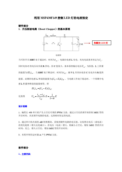
1、系统功能框图
2芯片资料:
MSP430F149:
低电源电压范围:1.8~3.6V
超低功耗:待机模式:1.6uA 关闭模式(RAM保持):0.1uA 活动模式:280uA at 1MHz,2.2V
5种省电模式
6us内从待机模式唤醒
16位RISC结构,125ns指令周期
带内部参考,采样保持和自动扫描特性的12位A/D转换器
有7个捕获/比较寄存器的16位定时器Timer_B 有3个捕获/比较寄存器的16位定时器Timer_A
片内集成比较器
串行在线编程,无需外部编程电压,安全熔丝可编程代码保护.
器件系列包括:–MSP430F133:8KB+256B闪速存储器,256B的RAM –MSP430F135:16KB+256B闪速存储器,512B的RAM –MSP430F147,MSP430F1471:32KB+256B闪速存储器,1KB的RAM –MSP430F148, MSP430F1481:48KB+256B闪速存储器,2KB的RAM –MSP430F149, MSP430F1491:60KB+256B闪速存储器,2KB的RAM
可用封装:64脚方形扁平封装(QFP).
功能框图。

自文档归原著所有LT-1BMSP430F149 学习板原理图技术文档说明:自文档归原著所有,但原理图部分有本人自己画图所得,将原著分开的文档画在一个工作区内,方便查阅。
MSP430F149学习板特点选用16 位超低功耗单片机MSP430F149,此MCU的特点如下:l 1.8V~3.6V超宽供电电压l 5 种低功耗模式,从standby 模式唤醒时间小于6μsl0.1uA RAM 保持l0.8uA 实时时钟模式l2K RAM,60KB+256B Flash Memory(支持IAP)l片内硬件乘法器支持四种乘法运算l两个具有PWM输出单元的16-Bit定时器(TimerA3,TimerB7)l两个UART接口,两个SPI 接口(与UART 复用)l一个8 通道12-Bit模数转换器(ADC),具有片内参考电压源l一个模拟比较器,看门狗电路等开发板上功能全面、板上资源丰富:¾三种可选供电方式(标准稳压器接口、USB 接口、电池接口)¾一个8-Bit 双向电平转换接口(5V--3.3V, 3.3V--5V)¾一个兼容USB2.0 规范、符合USB1.1 规范的标准USB 接口¾一个标准的六芯PS2 接口¾一个符合原厂标准的JTAG 仿真调试端口¾一个蜂鸣器¾一个射频通信模块接口¾一个12-Bit 高精度温度传感器¾一个8 路12-Bit 模数转换器(ADC)接口¾一个标准的1602 液晶接口¾一个标准的12864液晶接口¾一个六位共阴极动态扫描数码管电路¾一个可更换的CPU适配器¾一个RTC实时时钟+纽扣电池¾一个存储容量为256×8-Bit的EEPROM¾一个单路输出8-Bit 数模转换器(DAC)¾一个4×4的矩阵式键盘¾一个4×1的独立式按键(与4×4 的矩阵式键盘复用)¾一个标准的RS232接口¾一个简易的RS485接口¾一个含8 个LED 的流水灯电路(红、黄、绿)¾MCU 的全部IO 都用插针引出,便于二次开发提供电源指示灯和上电自动复位、手动复位电路,全SMD 设计、系统稳定可靠。


MSP430F149的ADC操作1)ADC图解图1 ADC的原理图理解:1.ADC的时钟来源可以有四个(ACLK/MCLK/SMCLK/ADC12SO)由ADC12SSELx来选择。
并且可以由ADC12DIVx控制选择分频。
2.ADC的采样参考电压可以由SREF0,SREF1来选择四种参考电压。
3.INCHx控制选择模拟电压输入口。
4.SHSx选择控制方式。
2)ADC的内核1.ADC的转换公式当采样最高电压高过或等于参考电压的时候,是最大值0FFFH。
当采样最低电压低于或是等于参考电压的时候,是最小值000H。
2.控制ADC12的内核可以通过ADC12CTL0和ADC12CTL1两个寄存器来控制。
当不使用的时候可以通过ADC12ON位来控制关闭内核以达到低功耗的目的。
当修改转换使能标志ENC的时候,要先判断ADC12内核是否在进行转换工作,如果在转换工作期间关闭ENC(置零)那么最终得到错误的结果。
3)ADC的时钟来源ADC可以有四种时钟来源。
而ADC12OSC是ADC内置的一个时钟源,大概频率在5MHZ左右,不过该时钟源由个人设备、供电电压和外部温度的影响很大。
4)ADC的参考电压发生器ADC内部可以提供一个可以产生1.5V或是2.5V的产考电压发生器。
当设计使用的时候,需要将一个10uF的电容和一个0.1uF的电容并联到它的输出端。
而且使用的时候,打开发生器至少需要等待17ms以让参考电压达到一个稳定的值。
5)ADC的低功耗当ADC内核不适用的时候,它会自动进入关闭模式,在使用的时候自动苏醒。
而它的参考电压却不会自动关闭,要用手通过REFON手动关闭。
6)ADC的采样保持触发源它的触发源由四种选择。
1.ADC12SC位控制。
2.定时器A输出控制3.定时器B输出控制4.定时器B输出控制7)ADC的采样保持时间ADC的采样保持时间有两种模式。
1.拓展型采样时钟模式。
这个时候,采样的时间由SHI决定,也就是当SHI上升沿的时候开始采样,下降沿的时候结束采样。
MSP430F149 开发板使用说明2009年09月第一章新手入门1.1 MSP430F149 学习板特点:选用16 位超低功耗单片机MSP430F149,采用子母双板分离设计,MCU 子板与集成外设母板通过插针座连接,使用灵活方便。
ØMCU 的全部IO都用插针引出,便于二次开发提供电源指示灯和上电自动复位、手动复位电路。
2、蜂鸣器实验(1)蜂鸣器1:单频音(步进变音调)(2)蜂鸣器2:奏乐(祝你平安)3、数码管实验(1)数码管1(显示0123)(2)数码管2(动态显示0~F)4、4×1 独立按键实验(1)键盘1:扫描数码管显示5、1602 液晶实验(1)1602 液晶1:动态字符显示(2)1602 液晶2:静态字符显示(3)1602 液晶3:内部时钟显示6、RS232 接口实验(1)RS232 接口1:MCU 发送数据PC 机显示(2)RS232 接口2:按键控制MCU 发送数据PC 机显示(3)RS232 接口3:PC 机发送数据MCU 液晶显示(4)RS232 接口4:MCU 回发接收到的PC 机数据7、RS485 接口实验(1)RS485 接口1:发送程序8、PS2 接口实验(1)PS2 接口1:PS2 控制1602 显示9、12-Bit 高精度温度传感器实验(1)温度传感器1:DS18B20 在液晶显示10、RTC 实时时钟实验(1)实时时钟1:DS1302 测试(2)实时时钟2:DS1302 电子钟11、2k Bit EEPROM 实验(1)EEPROM1:AT24C02 测试(2)EEPROM2:读出数据通过串口在PC 机显示12、12-Bit 模数转换器(ADC)接口实验(1)模数转换器2:ADC 在1602 液晶在显示(2)模数转换器3:ADC 通过串口在PC 机显示13、12864 液晶实验(与12864 液晶配套)(1)12864 液晶并口1:字符显示(2)12864 液晶并口2:汉字显示(3)12864 液晶并口3:图形显示(4)12864 液晶并口4:综合演示(5)12864 液晶串口5:字符显示(6)12864 液晶串口6:汉字显示(7)12864 液晶串口7:图形显示(8)12864 液晶串口8:综合演示14、HS0038红外接口实验(1)红外遥控解码实验,在数码管上显示三、开发板综合程序1、温度时间综合实验(1)DS18B20 + DS1302 + 16022、SSCOM综合实验(1)PC发送接收字符第三章板上资源详解本章详细介绍了MSP430F149 学习板上各个功能模块的硬件电路原理、使用方法和注意事项,使用前请仔细阅读。
MSP430F149的存储器结构及FLASH读写1 概述1.1 FLASH特点写操作只能将1改写为0,不能将0改写成1。
FLASH擦除后所有单元变为1,擦除操作只能针对整个段。
FLASH在擦除前不能被改写。
1.2 MSP430F149存储器编址方式MSP430F149的ROM为60K+256B的FLASH,RAM为2K。
MSP430存储器采用冯诺依曼结构,RAM和ROM合在一起编址。
MSP430F149内部集成有FLASH控制器,可以简化对FLASH的操作。
64K的寻址空间分为RAM、FLASH。
RAM分两块:1、寄存器(0000H-01FFH),存放特殊寄存器、设备寄存器、变量与堆栈。
2、数据RAM(01FFH-),存放各种变量、中间结果、堆栈。
FLASH分两块:1、主FLASH 一般用于存放程序代码。
2、信息FLASH(InfoFlash)用作掉电后保存少量数据。
分为InfoA(0X1080-0X10FF)和InfoB(0X1000-0X1080),每段各128B。
1.3 操作三种操作:读取、擦除(只能针对段擦除)、写入(可以写入单个字节)。
2使用方法2.1 程序架构读取FLASH方法和读取RAM方法相同。
写和擦除FLASH要进行如下配置:配置寄存器制定指针地址写数据/复制数据配置寄存器2.2 参数配置主要配置三个寄存器FCTL1,FCTL2,FCTL3。
1、配置FLASH控制器时钟。
时钟要求控制在250-470Khz之间。
FCTL2 = FWKEY + FSSEL0 + FN0; //2分频2、用指针指向地址Unsigned char *ptr= (unsigned char *) 0x1080;3、进入写模式或擦除模式FCTL1=FWKEY+WRT;或FCTL1=FWKEY+ERASE4、清除锁定位FCTL3=FWKEY;5、写数据*ptr=0x30;或擦除*ptr=0;6、退出写状态,恢复锁存FCTL1=FWKEY;FCTL3=FWKEY+LOCK;2.3 说明上电FLASH默认状态是读。
An IMPORTANT NOTICE at the end of this data sheet addresses availability,warranty,changes,use in safety-critical applications,intellectual property matters and other important disclaimers.PRODUCTION DATA.MSP430F149,MSP430F148,MSP430F147MSP430F1491,MSP430F1481,MSP430F1471MSP430F135,MSP430F133SLAS272H –JULY 2000–REVISED MAY 20181Device Overview1.1Features•Low Supply Voltage Range,1.8V to 3.6V •Ultra-Low Power Consumption:–Active Mode:280µA at 1MHz,2.2V –Standby Mode:1.6µA–Off Mode (RAM Retention):0.1µA •Five Power-Saving Modes•Wakeup From Standby Mode in Less Than 6µs •16-Bit RISC Architecture,125-ns Instruction Cycle Time•12-Bit Analog-to-Digital Converter (ADC)With Internal Reference,Sample-and-Hold,and Autoscan Feature•16-Bit Timer_B With Seven Capture/Compare-With-Shadow Registers•16-Bit Timer_A With Three Capture/Compare Registers•On-Chip Comparator•Serial Onboard Programming,No External Programming Voltage Needed,Programmable Code Protection by Security Fuse•Serial Communication Interface (USART),Functions as Asynchronous UART or Synchronous SPI Interface–Two USARTs (USART0,USART1)On MSP430F14x and MSP430F14x1Devices –One USART (USART0)On MSP430F13x Devices•Family Members (Also See Device Comparison )–MSP430F133–8KB +256Bytes of Flash Memory,256Bytes of RAM –MSP430F135–16KB +256Bytes of Flash Memory,512Bytes of RAM–MSP430F147,MSP430F1471–32KB +256Bytes of Flash Memory,1KB of RAM–MSP430F148,MSP430F1481–48KB +256Bytes of Flash Memory,2KB of RAM–MSP430F149,MSP430F1491–60KB +256Bytes of Flash Memory,2KB of RAM 1.2Applications•Sensor Systems •Industrial Controls•Hand-Held Meters1.3DescriptionThe Texas Instruments MSP430™family of ultra-low-power microcontrollers (MCUs)consist of several devices featuring different sets of peripherals targeted for various applications.The architecture,combined with five low-power modes is optimized to achieve extended battery life in portable measurement applications.The device features a powerful 16-bit RISC CPU,16-bit registers,and constant generators that attribute to maximum code efficiency.The digitally controlled oscillator (DCO)allows wake-up from low-power modes to active mode in less than 6µs.The MSP430F13x,MSP430F14x,and MSP430F14x1MCUs support two built-in 16-bit timers,a fast 12-bit ADC on the MSP430F13x and the MSP430F14x devices,one USART on the MSP430F13x devices or two USARTs on the MSP430F14x and MSP430F14x1devices,and 48I/O pins.The hardware multiplier enhances the performance and offers a broad code and hardware-compatible family solution.For complete module descriptions,see the MSP430x1xx Family User’s Guide .XT2IN XT2OUTTMS TCK TDI/TCLK TDO/TDIRST/NMIR 2MSP430F149,MSP430F148,MSP430F147MSP430F1491,MSP430F1481,MSP430F1471MSP430F135,MSP430F133SLAS272H –JULY 2000–REVISED MAY 2018Device Overview Copyright ©2000–2018,Texas Instruments Incorporated(1)For the most current device,package,and ordering information,see the Package Option Addendum in Section 8,or see the TI website at .(2)The sizes shown here are approximations.For the package dimensions with tolerances,see the Mechanical Data in Section 8.Device Information (1)PART NUMBERPACKAGE BODY SIZE (2)MSP430F149IPM LQFP (64)10mm ×10mm MSP430F149IPAG TQFP (64)10mm ×10mm MSP430F1491IRTD VQFN (64)9mm ×9mm1.4Functional Block DiagramsFigure 1-1shows the functional block diagram for the MSP430F13x MCUs.Figure 1-1.Functional Block Diagram,MSP430F13xXT2OUTTMS TCK TDI/TCLK TDO/TDIRST/NMIRR 3MSP430F149,MSP430F148,MSP430F147MSP430F1491,MSP430F1481,MSP430F1471MSP430F135,MSP430F133SLAS272H –JULY 2000–REVISED MAY 2018Device Overview Copyright ©2000–2018,Texas Instruments Incorporated Figure 1-2.Functional Block Diagram,MSP430F14xFigure 1-3shows the functional block diagram for the MSP430F14x1MCUs.Figure 1-3.Functional Block Diagram,MSP430F14x14MSP430F149,MSP430F148,MSP430F147MSP430F1491,MSP430F1481,MSP430F1471MSP430F135,MSP430F133SLAS272H –JULY 2000–REVISED MAY 2018Table of Contents Copyright ©2000–2018,Texas Instruments IncorporatedTable of Contents1Device Overview (1)1.1Features ..............................................11.2Applications ...........................................11.3Description ............................................11.4Functional Block Diagrams (2)2Revision History .........................................53Device Comparison . (6)3.1Related Products (6)4Terminal Configuration and Functions (7)4.1Pin Diagrams .........................................74.2Signal Descriptions (105)Specifications (16)5.1Absolute Maximum Ratings (16)5.2ESD Ratings........................................165.3Recommended Operating Conditions ...............165.4Supply Current Into AV CC and DV CC ExcludingExternal Current .....................................175.5Thermal Resistance Characteristics ................185.6Schmitt-Trigger Inputs –Ports P1,P2,P3,P4,P5,and P6...............................................185.7Standard Inputs –RST/NMI,JTAG (TCK,TMS,TDI/TCLK,TDO/TDI)...............................185.8Inputs –Px.y,TAx,TBx............................185.9Leakage Current ....................................195.10Outputs –Ports P1,P2,P3,P4,P5,and P6.......195.11Output Frequency ..................................195.12Typical Characteristics –Ports P1,P2,P3,P4,P5,and P6Outputs (20)5.13Wake-up Time From LPM3.........................215.14RAM .................................................215.15Comparator_A .......................................215.16Typical Characteristics –Comparator_A ............225.17PUC and POR ......................................235.18DCO Frequency .....................................245.19DCO When Using R OSC .............................255.20Crystal Oscillator,LFXT1...........................265.21Crystal Oscillator,XT2..............................265.22USART0,USART1..................................265.2312-Bit ADC,Power Supply and Input RangeConditions ...........................................275.2412-Bit ADC,External Reference ....................275.2512-Bit ADC,Built-In Reference . (28)5.2612-Bit ADC,Timing Parameters....................305.2712-Bit ADC,Linearity Parameters ...................305.2812-Bit ADC,Temperature Sensor and Built-In V MID315.29Flash Memory .......................................315.30JTAG Interface ......................................325.31JTAG Fuse.........................................326Detailed Description (33)6.1CPU .................................................336.2Instruction set .......................................346.3Operating Modes ....................................346.4Interrupt Vector Addresses ..........................356.5Bootloader (BSL)....................................356.6JTAG Fuse Check Mode ............................366.7Memory ..............................................366.8Peripherals ..........................................406.9Input/Output Diagrams (48)7Device and Documentation Support (59)7.1Getting Started and Next Steps .....................597.2Device Nomenclature ...............................597.3Tools and Software .................................617.4Documentation Support .............................627.5Related Links ........................................637.6Community Resources ..............................637.7Trademarks ..........................................637.8Electrostatic Discharge Caution .....................647.9Export Control Notice ...............................647.10Glossary .............................................648Mechanical,Packaging,and OrderableInformation (65)5MSP430F149,MSP430F148,MSP430F147MSP430F1491,MSP430F1481,MSP430F1471MSP430F135,MSP430F133SLAS272H –JULY 2000–REVISED MAY 2018Revision History Copyright ©2000–2018,Texas Instruments Incorporated 2Revision HistoryNOTE:Page numbers for previous revisions may differ from page numbers in the current version.Changes from February 12,2009to May 23,2018Page•Document format and organization changes throughout ........................................................................1•Added Section 1.2,Applications ....................................................................................................1•Added Section 3,Device Comparison ............................................................................................6•Added Section 5.2,ESD Ratings ..................................................................................................16•Removed note (2)with duplicate information from the f LFXT1parameter in Section 5.3,Recommended OperatingConditions ...........................................................................................................................16•Removed duplicate conditions "XTS =0,SELM =0or 1"from the second row of Test Conditions on the I (AM)parameter in Section 5.4,Supply Current Into AV CC and DV CC Excluding External Current ..............................17•Added Section 5.5,Thermal Resistance Characteristics ......................................................................18•Removed ADC12DIV from the equation in the TYP value of the t CONVERT parameter (because ADC12CLK isafter division)in Section 5.26,12-Bit ADC,Timing Parameters ..............................................................30•Changed all instances of bootstrap loader to bootloader throughout document ............................................35•Added Section 7,Device and Documentation Support (59)6MSP430F149,MSP430F148,MSP430F147MSP430F1491,MSP430F1481,MSP430F1471MSP430F135,MSP430F133SLAS272H –JULY 2000–REVISED MAY 2018Device Comparison Copyright ©2000–2018,Texas Instruments Incorporated(1)For the most current package and ordering information,see the Package Option Addendum in Section 8,or see the TI website at.(2)Package drawings,thermal data,and symbolization are available at .(3)Each number in the sequence represents an instantiation of Timer_A with its associated number of capture/compare registers and PWM output generators available.For example,a number sequence of 3,5would represent two instantiations of Timer_A,the first instantiation having 3and the second instantiation having 5capture/compare registers and PWM output generators,respectively.(4)Each number in the sequence represents an instantiation of Timer_B with its associated number of capture/compare registers and PWM output generators available.For example,a number sequence of 3,5would represent two instantiations of Timer_B,the first instantiation having 3and the second instantiation having 5capture/compare registers and PWM output generators,respectively.3Device ComparisonTable 3-1summarizes the features of the device variants in this data sheet.Table 3-1.Device Comparison (1)(2)Device Flash SRAM Timer_A (3)Timer_B (4)USART COMP_AADC12(Channels)I/Os Package MSP430F14960KB 2KB 372184864-pin PM 64-pin PAG 64-pin RTD MSP430F149160KB 2KB 372184864-pin PM 64-pin RTD MSP430F14848KB 2KB 372184864-pin PM 64-pin PAG 64-pin RTD MSP430F148148KB 2KB 372184864-pin PM 64-pin RTD MSP430F14732KB 1KB 372184864-pin PM 64-pin PAG 64-pin RTD MSP430F147132KB 1KB 372184864-pin PM 64-pin RTD MSP430F13516KB512bytes331184864-pin PM 64-pin PAG 64-pin RTD MSP430F1338KB 256bytes 331184864-pin PM 64-pin PAG 64-pin RTD3.1Related ProductsFor information about other devices in this family of products or related products,see the following links.TI 16-bit and 32-bit microcontrollers High-performance,low-power solutions to enable the autonomousfuture Products for MSP430ultra-low-power microcontrollersOne platform.One ecosystem.Endlesspossibilities.Products for other MSP430microcontrollers MCUs for metrology,monitoring,system control,andcommunications Companion Products for MSP430F149Review products that are frequently purchased or used with thisproduct.Reference Designs The TI Designs Reference Design Library is a robust reference design library thatspans analog,embedded processor,and connectivity.Created by TI experts to help you jump start your system design,all TI Designs include schematic or block diagrams,BOMs,and design files to speed your time to market.171819P5.4/MCLK P5.3P5.2P5.1P5.0P4.7/TBCLK P4.6P4.5P4.4P4.3P4.2/TB2P4.1/TB1P4.0/TB0P3.7P3.6P3.5/URXD0484746454443424140393837363534332012345678910111213141516DV CC P6.3/A3P6.4/A4P6.5/A5P6.6/A6P6.7/A7V REF+XIN XOUT Ve REF+V REF−/Ve REF−P1.0/TACLK P1.1/TA0P1.2/TA1P1.3/TA2P1.4/SMCLK21222324P 5.6/A C L K T D O /T D I 63626160596458A V P 6.2/A 2P 6.1/A 1P 6.0/A 0R S T /N M I T C K T M S P 2.6/A D C 12C L K P 2.7/T A 0P 3.0/S T E 0P 3.1/S I M O 0P 1.7/T A 2P 2.1/T A I N C L K P 2.2/C A O U T /T A 0P 2.3/C A 0/T A 1P 2.4/C A 1/T A 2P 2.5/R o s c 5655545725262728295352P 1.5/T A 0X T 2I N X T 2O U T 515049303132P 3.2/S O M I 0P 3.3/U C L K 0P 3.4/U T X D 0P 5.7/T B O U T HT D I /T C L K P 5.5/S M C L KA V D V P 1.6/T A 1P 2.0/A C L K C CS SS S7MSP430F149,MSP430F148,MSP430F147MSP430F1491,MSP430F1481,MSP430F1471MSP430F135,MSP430F133SLAS272H –JULY 2000–REVISED MAY 2018Terminal Configuration and Functions Copyright ©2000–2018,Texas Instruments Incorporated 4Terminal Configuration and Functions4.1Pin DiagramsFigure 4-1shows the pinout for the MSP430F133and MSP430F135MCUs in the 64-pin PM,PAG,and RTD packages.Figure 4-1.64-Pin PM,PAG,or RTD Package (Top View)for MSP430F133and MSP430F135171819P5.4/MCLK P5.3/UCLK1P5.2/SOMI1P5.1/SIMO1P5.0/STE1P4.7/TBCLK P4.6/TB6P4.5/TB5P4.4/TB4P4.3/TB3P4.2/TB2P4.1/TB1P4.0/TB0P3.7/URXD1P3.6/UTXD1P3.5/URXD0484746454443424140393837363534332012345678910111213141516DV CC P6.3/A3P6.4/A4P6.5/A5P6.6/A6P6.7/A7V REF+XIN XOUT Ve REF+V REF−/Ve REF−P1.0/TACLK P1.1/TA0P1.2/TA1P1.3/TA2P1.4/SMCLK21222324P 5.6/A C L K T D O /T D I 63626160596458A V P 6.2/A 2P 6.1/A 1P 6.0/A 0R S T /N M I T C K T M S P 2.6/A D C 12C L K P 2.7/T A 0P 3.0/S T E 0P 3.1/S I M O 0P 1.7/T A 2P 2.1/T A I N C L K P 2.2/C A O U T /T A 0P 2.3/C A 0/T A 1P 2.4/C A 1/T A 2P 2.5/R o s c 5655545725262728295352P 1.5/T A 0X T 2I N X T 2O U T 515049303132P 3.2/S O M I 0P 3.3/U C L K 0P 3.4/U T X D 0P 5.7/T B O U T HT D I /T C L K P 5.5/S M C L KA V D V P 1.6/T A 1P 2.0/A C L K C CS SS S8MSP430F149,MSP430F148,MSP430F147MSP430F1491,MSP430F1481,MSP430F1471MSP430F135,MSP430F133SLAS272H –JULY 2000–REVISED MAY 2018Terminal Configuration and FunctionsCopyright ©2000–2018,Texas Instruments IncorporatedFigure 4-2shows the pinout for the MSP430F147,MSP430F148,and MSP430F149MCUs in the 64-pin PM,PAG,and RTD packages.Figure 4-2.64-Pin PM,PAG,or RTD Package (Top View)for MSP430F147,MSP430F148,and MSP430F149171819P5.4/MCLK P5.3/UCLK1P5.2/SOMI1P5.1/SIMO1P5.0/STE1P4.7/TBCLK P4.6/TB6P4.5/TB5P4.4/TB4P4.3/TB3P4.2/TB2P4.1/TB1P4.0/TB0P3.7/URXD1P3.6/UTXD1P3.5/URXD0484746454443424140393837363534332012345678910111213141516DV CC P6.3P6.4P6.5P6.6P6.7ReservedXIN XOUT DV SS DV SSP1.0/TACLK P1.1/TA0P1.2/TA1P1.3/TA2P1.4/SMCLK21222324P 5.6/A C L K T D O /T D I 63626160596458A V P 6.2P 6.1P 6.0R S T /N M I T C K T M S P 2.6P 2.7/T A 0P 3.0/S T E 0P 3.1/S I M O 0P 1.7/T A 2P 2.1/T A I N C L K P 2.2/C A O U T /T A 0P 2.3/C A 0/T A 1P 2.4/C A 1/T A 2P 2.5/R o s c 5655545725262728295352P 1.5/T A 0X T 2I N X T 2O U T 515049303132P 3.2/S O M I 0P 3.3/U C L K 0P 3.4/U T X D 0P 5.7/T B O U T HT D I /T C L K P 5.5/S M C L KA V D V P 1.6/T A 1P 2.0/A C L K C CS SS S9MSP430F149,MSP430F148,MSP430F147MSP430F1491,MSP430F1481,MSP430F1471MSP430F135,MSP430F133SLAS272H –JULY 2000–REVISED MAY 2018Terminal Configuration and Functions Copyright ©2000–2018,Texas Instruments Incorporated Figure 4-3shows the pinout for the MSP430F1471,MSP430F1481,and MSP430F1491MCUs in the 64-pin PM and RTD packages.Figure 4-3.64-Pin PM or RTD Package (Top View)for MSP430F1471,MSP430F1481,and MSP430F149110MSP430F149,MSP430F148,MSP430F147MSP430F1491,MSP430F1481,MSP430F1471MSP430F135,MSP430F133SLAS272H –JULY 2000–REVISED MAY 2018Terminal Configuration and FunctionsCopyright ©2000–2018,Texas Instruments Incorporated4.2Signal DescriptionsTable 4-1describes the signals for the MSP430F13x and MSP430F14x MCUs.See Table 4-2for the MSP430F14x1signal descriptions.Table 4-1.Signal Descriptions for MSP430F13x and MSP430F14xSIGNAL NAME PIN NO.I/O DESCRIPTIONAV CC 64Analog supply voltage,positive terminal.Supplies the analog portion of the ADC.AV SS 62Analog supply voltage,negative terminal.Supplies the analog portion of the ADC.DV CC 1Digital supply voltage,positive terminal.Supplies all digital parts.DV SS63Digital supply voltage,negative terminal.Supplies all digital parts.P1.0/TACLK 12I/O General-purpose digital I/O pin Timer_A,clock signal TACLK inputP1.1/TA013I/OGeneral-purpose digital I/O pinTimer_A,capture:CCI0A input,compare:Out0output BSL transmitP1.2/TA114I/O General-purpose digital I/O pinTimer_A,capture:CCI0A input,compare:Out0output BSL transmitP1.3/TA215I/O General-purpose digital I/O pinTimer_A,capture:CCI2A input,compare:Out2output P1.4/SMCLK 16I/O General-purpose digital I/O pin SMCLK signal outputP1.5/TA017I/O General-purpose digital I/O pin Timer_A,compare:Out0output P1.6/TA118I/O General-purpose digital I/O pin Timer_A,compare:Out1output P1.7/TA219I/O General-purpose digital I/O pin Timer_A,compare:Out2output/P2.0/ACLK 20I/O General-purpose digital I/O pin ACLK outputP2.1/TAINCLK21I/OGeneral-purpose digital I/O pin Timer_A,clock signal at INCLK P2.2/CAOUT/TA022I/OGeneral-purpose digital I/O pin Comparator_A outputTimer_A,capture:CCI0B input BSL receiveP2.3/CA0/TA123I/OGeneral-purpose digital I/O pin Timer_A,compare:Out1output Comparator_A inputP2.4/CA1/TA224I/O General-purpose digital I/O pin Timer_A,compare:Out2output Comparator_A inputP2.5/R OSC 25I/O General-purpose digital I/O pininput for external resistor defining the DCO nominal frequency P2.6/ADC12CLK 26I/O General-purpose digital I/O pin Conversion clock for ADC P2.7/TA027I/O General-purpose digital I/O pin Timer_A,compare:Out0outputP3.0/STE028I/O General-purpose digital I/O pinSlave transmit enable for USART0in SPI mode P3.1/SIMO029I/O General-purpose digital I/O pinSlave in/master out of USART0in SPI mode P3.2/SOMI030I/O General-purpose digital I/O pinSlave out/master in of USART0in SPI modeP3.3/UCLK031I/O General-purpose digital I/OUSART0clock:external input in UART or SPI mode,output in SPI mode P3.4/UTXD032I/OGeneral-purpose digital I/O pinTransmit data out for USART0in UART mode11MSP430F149,MSP430F148,MSP430F147MSP430F1491,MSP430F1481,MSP430F1471MSP430F135,MSP430F133SLAS272H –JULY 2000–REVISED MAY 2018Terminal Configuration and Functions Copyright ©2000–2018,Texas Instruments IncorporatedTable 4-1.Signal Descriptions for MSP430F13x and MSP430F14x (continued)SIGNAL NAMEPIN NO.I/O DESCRIPTION (1)MSP430F14x devices onlyP3.5/URXD033I/O General-purpose digital I/O pin Receive data in for USART0in UART mode P3.6/UTXD1(1)34I/O General-purpose digital I/O pin Transmit data out for USART1in UART mode P3.7/URXD1(1)35I/O General-purpose digital I/O pin Receive data in for USART1in UART mode P4.0/TB0.36I/O General-purpose digital I/O pin Timer_B,capture:CCI0A or CCI0B input,compare:Out0output P4.1/TB137I/O General-purpose digital I/O pin Timer_B,capture:CCI1A or CCI1B input,compare:Out1output P4.2/TB238I/O General-purpose digital I/O pin Timer_B,capture:CCI2A or CCI2B input,compare:Out2output P4.3/TB3(1)39I/O General-purpose digital I/O pin Timer_B,capture:CCI3A or CCI3B input,compare:Out3output P4.4/TB4(1)40I/O General-purpose digital I/O pin Timer_B,capture:CCI4A or CCI4B input,compare:Out4output P4.5/TB5(1)41I/O General-purpose digital I/O pin Timer_B,capture:CCI5A or CCI5B input,compare:Out5output P4.6/TB6(1)42I/O General-purpose digital I/O pin Timer_B,capture:CCI6A or CCI6B input,compare:Out6output P4.7/TBCLK43I/O General-purpose digital I/O pin Timer_B,clock signal TBCLK input P5.0/STE1(1)44I/O General-purpose digital I/O pin Slave transmit enable for USART1in SPI mode P5.1/SIMO1(1)45I/O General-purpose digital I/O pin Slave in/master out of USART1in SPI mode P5.2/SOMI1(1)46I/O General-purpose digital I/O pin Slave out/master in of USART1in SPI mode P5.3/UCLK1(1)47I/O General-purpose digital I/O pin USART1clock:external input in UART or SPI mode,output in SPI mode P5.4/MCLK48I/O General-purpose digital I/O pin Main system clock MCLK output P5.5/SMCLK49I/O General-purpose digital I/O pin Submain system clock SMCLK output P5.6/ACLK50I/O General-purpose digital I/O pin Auxiliary clock ACLK output P5.7/TBOUTH51I/O General-purpose digital I/O pin Switch all PWM digital output ports to high impedance for Timer_B7(TB0to TB6)P6.0/A059I/O General-purpose digital I/O pin Analog input A0for ADC P6.1/A160I/O General-purpose digital I/O pin Analog input A1for ADC P6.2/A261I/O General-purpose digital I/O pin Analog input A2for ADC P6.3/A32I/O General-purpose digital I/O pin Analog input A3for ADC P6.4/A43I/O General-purpose digital I/O pin Analog input A4for ADC P6.5/A54I/O General-purpose digital I/O pin Analog input A5for ADC P6.6/A65I/O General-purpose digital I/O pin Analog input A6for ADC P6.7/A76I/O General-purpose digital I/O pinAnalog input A7for ADC12MSP430F149,MSP430F148,MSP430F147MSP430F1491,MSP430F1481,MSP430F1471MSP430F135,MSP430F133SLAS272H –JULY 2000–REVISED MAY 2018Terminal Configuration and Functions Copyright ©2000–2018,Texas Instruments IncorporatedTable 4-1.Signal Descriptions for MSP430F13x and MSP430F14x (continued)SIGNAL NAMEPIN NO.I/O DESCRIPTION RST/NMI58I Reset input Nonmaskable interrupt input port Bootloader start TCK57I Test clock,the clock input port for device programming test and bootloader start TDI/TCLK55I Test data input or test clock input.The device protection fuse is connected to TDI/TCLK.TDO/TDI54I/O Test data output or programming data input TMS56I Test mode select,used as an input port for device programming and test VeREF+10I Input for an external reference voltage to the ADC VREF+7O Output of positive terminal of the reference voltage in the ADC VREF −/VeREF −11I Negative terminal for the ADC reference voltage for both sources,the internal reference voltage or an external applied reference voltage XIN8I Input port for crystal oscillator XT1,standard or watch crystals can be connected XOUT9O Output terminal of crystal oscillator XT1XT2IN53I Input port for crystal oscillator XT2,only standard crystals can be connected XT2OUT52O Output terminal of crystal oscillator XT2QFN Pad NA NA QFN package pad,connect to DV SS13MSP430F149,MSP430F148,MSP430F147MSP430F1491,MSP430F1481,MSP430F1471MSP430F135,MSP430F133SLAS272H –JULY 2000–REVISED MAY 2018Terminal Configuration and Functions Copyright ©2000–2018,Texas Instruments Incorporated Table 4-2describes the signals for the MSP430F14x1MCUs.See Table 4-1for the MSP430F13x and MSP430F14x signal descriptions.Table 4-2.Signal Descriptions for MSP430F14x1SIGNAL NAMEPIN NO.I/O DESCRIPTION AV CC64Analog supply voltage positive terminal AV SS62Analog supply voltage negative terminal DV CC1Digital supply voltage,positive terminal.Supplies all digital parts.DV SS63Digital supply voltage,negative terminal.Supplies all digital parts.P1.0/TACLK12I/O General-purpose digital I/O pin Timer_A,clock signal TACLK input P1.1/TA013I/O General-purpose digital I/O pin Timer_A,capture:CCI0A input,compare:Out0output BSL transmit P1.2/TA114I/O General-purpose digital I/O pin Timer_A,capture:CCI1A input,compare:Out1output P1.3/TA215I/O General-purpose digital I/O pin Timer_A,capture:CCI2A input,compare:Out2output P1.4/SMCLK16I/O General-purpose digital I/O pin SMCLK signal output P1.5/TA017I/O General-purpose digital I/O pin Timer_A,compare:Out0output P1.6/TA118I/O General-purpose digital I/O pin Timer_A,compare:Out1output P1.7/TA219I/O General-purpose digital I/O pin Timer_A,compare:Out2output P2.0/ACLK20I/O General-purpose digital I/O pin ACLK output P2.1/TAINCLK 21I/O General-purpose digital I/O pinTimer_A,clock signal at INCLKP2.2/CAOUT/TA022I/O General-purpose digital I/O pinTimer_A,capture:CCI0B inputComparator_A outputBSL receiveP2.3/CA0/TA123I/O General-purpose digital I/O pinTimer_A,compare:Out1outputComparator_A inputP2.4/CA1/TA224I/O General-purpose digital I/O pinTimer_A,compare:Out2outputComparator_A inputP2.5/R OSC 25I/O General-purpose digital I/O pinInput for external resistor defining the DCO nominal frequencyP2.626I/O General-purpose digital I/O pinP2.7/TA027I/O General-purpose digital I/O pinTimer_A,compare:Out0outputP3.0/STE028I/O General-purpose digital I/O pinSlave transmit enable for USART0in SPI modeP3.1/SIMO029I/O General-purpose digital I/O pinSlave in/master out of USART0in SPI modeP3.2/SOMI030I/O General-purpose digital I/O pinSlave out/master in of USART0in SPI modeP3.3/UCLK031I/O General-purpose digital I/OUSART0clock:external input in UART or SPI mode,output in SPI modeP3.4/UTXD032I/O General-purpose digital I/O pinTransmit data out for USART0in UART modeP3.5/URXD033I/OGeneral-purpose digital I/O pinReceive data in for USART0in UART mode14MSP430F149,MSP430F148,MSP430F147MSP430F1491,MSP430F1481,MSP430F1471MSP430F135,MSP430F133SLAS272H –JULY 2000–REVISED MAY 2018Terminal Configuration and FunctionsCopyright ©2000–2018,Texas Instruments Incorporated Table 4-2.Signal Descriptions for MSP430F14x1(continued)SIGNAL NAMEPIN NO.I/O DESCRIPTION P3.6/UTXD134I/O General-purpose digital I/O pin Transmit data out for USART1in UART mode P3.7/URXD135I/O General-purpose digital I/O pin Receive data in for USART1in UART mode P4.0/TB0.36I/O General-purpose digital I/O pin Timer_B,capture:CCI0A or CCI0B input,compare:Out0output P4.1/TB137I/O General-purpose digital I/O pin Timer_B,capture:CCI1A or CCI1B input,compare:Out1output P4.2/TB238I/O General-purpose digital I/O pin Timer_B,capture:CCI2A or CCI2B input,compare:Out2output P4.3/TB339I/O General-purpose digital I/O pin Timer_B,capture:CCI3A or CCI3B input,compare:Out3output P4.4/TB440I/O General-purpose digital I/O pin Timer_B,capture:CCI4A or CCI4B input,compare:Out4output P4.5/TB541I/O General-purpose digital I/O pin Timer_B,capture:CCI5A or CCI5B input,compare:Out5output P4.6/TB642I/O General-purpose digital I/O pin Timer_B,capture:CCI6A or CCI6B input,compare:Out6output P4.7/TBCLK43I/O General-purpose digital I/O pin Timer_B,clock signal TBCLK input P5.0/STE144I/O General-purpose digital I/O pin Slave transmit enable for USART1in SPI mode P5.1/SIMO145I/O General-purpose digital I/O pin Slave in/master out of USART1in SPI mode P5.2/SOMI146I/O General-purpose digital I/O pin Slave out/master in of USART1in SPI mode P5.3/UCLK147I/O General-purpose digital I/O pin USART1clock:external input in UART or SPI mode,output in SPI mode P5.4/MCLK48I/O General-purpose digital I/O pin Main system clock MCLK output P5.5/SMCLK49I/O General-purpose digital I/O pin Submain system clock SMCLK output P5.6/ACLK50I/O General-purpose digital I/O pin Auxiliary clock ACLK output P5.7/TBOUTH51I/O General-purpose digital I/O pin Switch all PWM digital output ports to high impedance for Timer_B7(TB0to TB6)P6.059I/O General-purpose digital I/O pin P6.160I/O General-purpose digital I/O pin P6.261I/O General-purpose digital I/O pin P6.32I/O General-purpose digital I/O pin P6.43I/O General-purpose digital I/O pin P6.54I/O General-purpose digital I/O pin P6.65I/O General-purpose digital I/O pin P6.76I/O General-purpose digital I/O pin RST/NMI58I Reset input Nonmaskable interrupt input port Bootloader start TCK57I Test clock,the clock input port for device programming test and bootloader start TDI/TCLK55I Test data input or test clock input.The device protection fuse is connected to TDI/TCLK.TDO/TDI54I/O Test data output or programming data input TMS56I Test mode select,used as an input port for device programming and test DV SS10I Connect to DV SS Reserved7Reserved,do not connect externally。