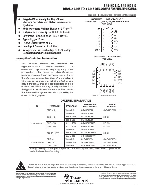
54AC139 74AC139双1-4线译码器 分配器
- 格式:pdf
- 大小:183.77 KB
- 文档页数:3


线译码器74LS154引脚,参数,及功能介绍--------------------------------------------------------------------------------4 线-16 线译码器74LS154/54LS154引脚图,参数,及功能介绍74ls154功能简介:54/74154 为4 线-16 线译码器,当选通端(G1、G2)均为低电平时,可将地址端(ABCD)的二进制编码在一个对应的输出端,以低电平译出。
如果将G1和G2中的一个作为数据输入端,由ABCD对输出寻址,74LS154还可作1线-16线数据分配器。
74LS154管脚图:引脚功能介绍A、B、C、D 译码地址输入端(低电平有效)G1、G2 选通端(低电平有效)0-15 输出端(低电平有效)74ls154真值表:推荐工作条件74ls154电气参数极限值电源电压: 7V输入电压: 5.5V工作环境温度54154:-55~125℃74154:0~70℃贮存温度:-65~150℃本文来自: 原文网址:/info/commonIC/0075219.html本文来自: 原文网址:/info/commonIC/0075219.html74ls154芯片资料2007-08-20 20:4874ls138译码器74ls139 跟74ls138类似,区别在于139内部是2个独立的2-4译码器。
74ls154跟74LS138很类似,差别就在于,138是3-8译码器,154是4-16译码器。
类别:集成块资料| 添加到搜藏| 分享到i贴吧| 浏览(1104) | 评论(1)上一篇:DDS芯片AD9850的工作原理及其与...下一篇:芯片的型号及功能最近读者:登录后,您就出现在这里。
有梦无花wangjunxiahah艺新。
PACKAGING INFORMATIONOrderable Device Status(1)PackageType PackageDrawingPins PackageQtyEco Plan(2)Lead/Ball Finish MSL Peak Temp(3)84092012A ACTIVE LCCC FK201TBD Call TI Level-NC-NC-NC 8409201EA ACTIVE CDIP J161TBD Call TI Level-NC-NC-NC 8409201FA ACTIVE CFP W161TBD Call TI Level-NC-NC-NCJM38510/65803BEA ACTIVE CDIP J161TBD Call TI Level-NC-NC-NCJM38510/65803BFA ACTIVE CFP W161TBD Call TI Level-NC-NC-NC SN54HC139J ACTIVE CDIP J161TBD Call TI Level-NC-NC-NC SN74HC139D ACTIVE SOIC D1640Green(RoHS&no Sb/Br)CU NIPDAU Level-1-260C-UNLIMSN74HC139DBR ACTIVE SSOP DB162000Green(RoHS&no Sb/Br)CU NIPDAU Level-1-260C-UNLIMSN74HC139DBRE4ACTIVE SSOP DB162000Green(RoHS&no Sb/Br)CU NIPDAU Level-1-260C-UNLIMSN74HC139DE4ACTIVE SOIC D1640Green(RoHS&no Sb/Br)CU NIPDAU Level-1-260C-UNLIMSN74HC139DR ACTIVE SOIC D162500Green(RoHS&no Sb/Br)CU NIPDAU Level-1-260C-UNLIMSN74HC139DRE4ACTIVE SOIC D162500Green(RoHS&no Sb/Br)CU NIPDAU Level-1-260C-UNLIMSN74HC139DT ACTIVE SOIC D16250Green(RoHS&no Sb/Br)CU NIPDAU Level-1-260C-UNLIMSN74HC139DTE4ACTIVE SOIC D16250Green(RoHS&no Sb/Br)CU NIPDAU Level-1-260C-UNLIMSN74HC139N ACTIVE PDIP N1625Pb-Free(RoHS)CU NIPDAU Level-NC-NC-NC SN74HC139N3OBSOLETE PDIP N16TBD Call TI Call TISN74HC139NSR ACTIVE SO NS162000Green(RoHS&no Sb/Br)CU NIPDAU Level-1-260C-UNLIMSN74HC139NSRE4ACTIVE SO NS162000Green(RoHS&no Sb/Br)CU NIPDAU Level-1-260C-UNLIMSN74HC139PW ACTIVE TSSOP PW1690Green(RoHS&no Sb/Br)CU NIPDAU Level-1-260C-UNLIMSN74HC139PWE4ACTIVE TSSOP PW1690Green(RoHS&no Sb/Br)CU NIPDAU Level-1-260C-UNLIMSN74HC139PWG4ACTIVE TSSOP PW1690Green(RoHS&no Sb/Br)CU NIPDAU Level-1-260C-UNLIM SN74HC139PWLE OBSOLETE TSSOP PW16TBD Call TI Call TISN74HC139PWR ACTIVE TSSOP PW162000Green(RoHS&no Sb/Br)CU NIPDAU Level-1-260C-UNLIMSN74HC139PWRE4ACTIVE TSSOP PW162000Green(RoHS&no Sb/Br)CU NIPDAU Level-1-260C-UNLIMSN74HC139PWRG4ACTIVE TSSOP PW162000Green(RoHS&no Sb/Br)CU NIPDAU Level-1-260C-UNLIMSN74HC139PWT ACTIVE TSSOP PW16250Green(RoHS&no Sb/Br)CU NIPDAU Level-1-260C-UNLIMSN74HC139PWTE4ACTIVE TSSOP PW16250Green(RoHS&no Sb/Br)CU NIPDAU Level-1-260C-UNLIMSN74HC139PWTG4ACTIVE TSSOP PW16250Green(RoHS&no Sb/Br)CU NIPDAU Level-1-260C-UNLIMOrderable Device Status(1)PackageType PackageDrawingPins PackageQtyEco Plan(2)Lead/Ball Finish MSL Peak Temp(3)SNJ54HC139FK ACTIVE LCCC FK201TBD Call TI Level-NC-NC-NC SNJ54HC139J ACTIVE CDIP J161TBD Call TI Level-NC-NC-NC SNJ54HC139W ACTIVE CFP W161TBD Call TI Level-NC-NC-NC(1)The marketing status values are defined as follows:ACTIVE:Product device recommended for new designs.LIFEBUY:TI has announced that the device will be discontinued,and a lifetime-buy period is in effect.NRND:Not recommended for new designs.Device is in production to support existing customers,but TI does not recommend using this part in a new design.PREVIEW:Device has been announced but is not in production.Samples may or may not be available.OBSOLETE:TI has discontinued the production of the device.(2)Eco Plan-The planned eco-friendly classification:Pb-Free(RoHS)or Green(RoHS&no Sb/Br)-please check /productcontent for the latest availability information and additional product content details.TBD:The Pb-Free/Green conversion plan has not been defined.Pb-Free(RoHS):TI's terms"Lead-Free"or"Pb-Free"mean semiconductor products that are compatible with the current RoHS requirements for all6substances,including the requirement that lead not exceed0.1%by weight in homogeneous materials.Where designed to be soldered at high temperatures,TI Pb-Free products are suitable for use in specified lead-free processes.Green(RoHS&no Sb/Br):TI defines"Green"to mean Pb-Free(RoHS compatible),and free of Bromine(Br)and Antimony(Sb)based flame retardants(Br or Sb do not exceed0.1%by weight in homogeneous material)(3)MSL,Peak Temp.--The Moisture Sensitivity Level rating according to the JEDEC industry standard classifications,and peak solder temperature.Important Information and Disclaimer:The information provided on this page represents TI's knowledge and belief as of the date that it is provided.TI bases its knowledge and belief on information provided by third parties,and makes no representation or warranty as to the accuracy of such information.Efforts are underway to better integrate information from third parties.TI has taken and continues to take reasonable steps to provide representative and accurate information but may not have conducted destructive testing or chemical analysis on incoming materials and chemicals.TI and TI suppliers consider certain information to be proprietary,and thus CAS numbers and other limited information may not be available for release.In no event shall TI's liability arising out of such information exceed the total purchase price of the TI part(s)at issue in this document sold by TI to Customer on an annual basis.IMPORTANT NOTICETexas Instruments Incorporated and its subsidiaries (TI) reserve the right to make corrections, modifications, enhancements, improvements, and other changes to its products and services at any time and to discontinue any product or service without notice. Customers should obtain the latest relevant information before placing orders and should verify that such information is current and complete. All products are sold subject to TI’s terms and conditions of sale supplied at the time of order acknowledgment.TI warrants performance of its hardware products to the specifications applicable at the time of sale in accordance with TI’s standard warranty. T esting and other quality control techniques are used to the extent TI deems necessary to support this warranty. Except where mandated by government requirements, testing of all parameters of each product is not necessarily performed.TI assumes no liability for applications assistance or customer product design. Customers are responsible for their products and applications using TI components. T o minimize the risks associated with customer products and applications, customers should provide adequate design and operating safeguards.TI does not warrant or represent that any license, either express or implied, is granted under any TI patent right, copyright, mask work right, or other TI intellectual property right relating to any combination, machine, or process in which TI products or services are used. Information published by TI regarding third-party products or services does not constitute a license from TI to use such products or services or a warranty or endorsement thereof. Use of such information may require a license from a third party under the patents or other intellectual property of the third party, or a license from TI under the patents or other intellectual property of TI.Reproduction of information in TI data books or data sheets is permissible only if reproduction is without alteration and is accompanied by all associated warranties, conditions, limitations, and notices. Reproduction of this information with alteration is an unfair and deceptive business practice. TI is not responsible or liable for such altered documentation.Resale of TI products or services with statements different from or beyond the parameters stated by TI for that product or service voids all express and any implied warranties for the associated TI product or service and is an unfair and deceptive business practice. TI is not responsible or liable for any such statements. Following are URLs where you can obtain information on other Texas Instruments products and application solutions:Products ApplicationsAmplifiers Audio /audioData Converters Automotive /automotiveDSP Broadband /broadbandInterface Digital Control /digitalcontrolLogic Military /militaryPower Mgmt Optical Networking /opticalnetwork Microcontrollers Security /securityTelephony /telephonyVideo & Imaging /videoWireless /wirelessMailing Address:Texas InstrumentsPost Office Box 655303 Dallas, Texas 75265Copyright 2005, Texas Instruments Incorporated。
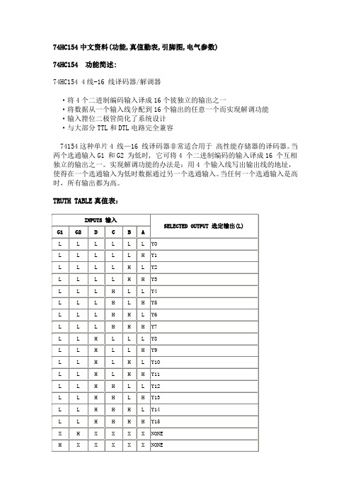
74HC154中文资料(功能,真值勤表,引脚图,电气参数)
74HC154 功能简述:
74HC154 4线-16 线译码器/解调器
·将4个二进制编码输入译成16个彼独立的输出之一
·将数据从一个输入线分配到16个输出的任意一个而实现解调功能
·输入箝位二极管简化了系统设计
·与大部分TTL和DTL电路完全兼容
74154这种单片4 线—16 线译码器非常适合用于高性能存储器的译码器。
当两个选通输入G1 和G2 为低时, 它可将4 个二进制编码的输入译成16 个互相独立的输出之一。
实现解调功能的办法是:用4 个输入线写出输出线的地址,使得在一个选通输入为低时数据通过另一个选通输入。
当任何一个选通输入是高时,所有输出都为高。
TRUTH TABLE真值表:
引脚功能表:
图1 引脚图
图2 国际电工委员会逻辑符号ABSOLUTE MAXIMUM RATINGS绝对最大额定值
RECOMMENDED OPERATING CONDITIONS建议操作条件
DC SPECIFICATIONS直流电气规格:
74HC154。
线译码器74LS154引脚,参数,及功能介绍
--------------------------------------------------------------------------------
4 线-16 线译码器 74LS154/54LS154引脚图,参数,及功能介绍
74ls154功能简介:
54/74154 为 4 线-16 线译码器,当选通端(G1、G2)均为低电平时,可将地址端(ABCD)的二进制编码在一个对应的输出端,以低电平译出。
如果将G1和G2中的一个作为数据输入端,由ABCD对输出寻址,74LS154还可作1线-16线数据分配器。
74LS154管脚图:
引脚功能介绍
A、B、C、D 译码地址输入端(低电平有效)
G1、G2 选通端(低电平有效)
0-15 输出端(低电平有效)
74ls154真值表:
推荐工作条件
74ls154电气参数
极限值
电源电压: 7V
输入电压:
工作环境温度
54154:-55~125℃
74154:0~70℃
贮存温度:-65~150℃
本文来自: 原文网址:
74ls154芯片资料
2007-08-20 20:48
74ls138译码器
74ls139 跟74ls138类似,区别在于139内部是2个独立的2-4译码器。
74ls154跟74LS138很类似,差别就在于,138是3-8译码器,154是4-16译码器。
| | | 浏览(1104) | ?(1)
上一篇:????下一篇:
最近读者:
后,您就
出现在
这里。
SO16:plastic small outline package; 16 leads; body width 3.9 mm SOT109-1SSOP16:plastic shrink small outline package; 16 leads; body width 5.3 mm SOT338-1TSSOP16:plastic thin shrink small outline package; 16 leads; body width 4.4 mm SOT403-1Philips Semiconductors and Philips Electronics North America Corporation reserve the right to make changes, without notice, in the products,including circuits, standard cells, and/or software, described or contained herein in order to improve design and/or performance. Philips Semiconductors assumes no responsibility or liability for the use of any of these products, conveys no license or title under any patent, copyright,or mask work right to these products, and makes no representations or warranties that these products are free from patent, copyright, or mask work right infringement, unless otherwise specified. Applications that are described herein for any of these products are for illustrative purposes only. Philips Semiconductors makes no representation or warranty that such applications will be suitable for the specified use without further testing or modification.LIFE SUPPORT APPLICATIONS Philips Semiconductors and Philips Electronics North America Corporation Products are not designed for use in life support appliances, devices,or systems where malfunction of a Philips Semiconductors and Philips Electronics North America Corporation Product can reasonably be expected to result in a personal injury. Philips Semiconductors and Philips Electronics North America Corporation customers using or selling Philips Semiconductors and Philips Electronics North America Corporation Products for use in such applications do so at their own risk and agree to fully indemnify Philips Semiconductors and Philips Electronics North America Corporation for any damages resulting from such improper use or sale.This data sheet contains preliminary data, and supplementary data will be published at a later date. PhilipsSemiconductors reserves the right to make changes at any time without notice in order to improve designand supply the best possible product.Philips Semiconductors811 East Arques AvenueP .O. Box 3409Sunnyvale, California 94088–3409Telephone 800-234-7381DEFINITIONSData Sheet IdentificationProduct Status Definition Objective Specification Preliminary Specification Product Specification Formative or in Design Preproduction Product Full ProductionThis data sheet contains the design target or goal specifications for product development. Specificationsmay change in any manner without notice.This data sheet contains Final Specifications. Philips Semiconductors reserves the right to make changesat any time without notice, in order to improve design and supply the best possible product.© Copyright Philips Electronics North America Corporation 1998All rights reserved. Printed in U.S.A.print codeDate of release: 05-96。
集成电路课程设计1. 目的与任务本课程设计是《集成电路分析与设计基础》的实践课程,其主要目的是使学生在熟悉集成电路制造技术、半导体器件原理和集成电路分析与设计基础上,训练综合运用已掌握的知识,利用相关软件,初步熟悉和掌握集成电路芯片系统设计→电路设计及模拟→版图设计→版图验证等正向设计方法。
2. 设计题目与要求2.1设计题目及其性能指标要求器件名称:含两个2-4译码器的74HC139芯片 要求电路性能指标:(1) 可驱动10个LSTTL 电路(相当于15pF 电容负载); (2) 输出高电平时,|I OH |≤20μA ,V OH ,min =4.4V ; (3) 输出底电平时,|I OL |≤4mA ,V OL ,man =0.4V ; (4) 输出级充放电时间t r =t f ,t pd <25ns ;(5) 工作电源5V ,常温工作,工作频率f work =30MHz ,总功耗P max =150mW 。
2.2设计要求1. 独立完成设计74HC139芯片的全过程;2. 设计时使用的工艺及设计规则: MOSIS:mhp_n12;3. 根据所用的工艺,选取合理的模型库;4. 选用以lambda(λ)为单位的设计规则;5. 全手工、层次化设计版图;6. 达到指导书提出的设计指标要求。
3. 设计方法与计算 3.1 74HC139芯片简介74HC139是包含两个2线-4线译码器的高速CMOS 数字电路集成芯片,能与TTL 集成电路芯片兼容,它的管脚图如图1所示,其逻辑真值表如表1所示:图1 74HC139芯片管脚图 表1 74HC139真值表片选 输入数据输出 C s A 1 A 0 Y 0 Y 1 Y 2 Y 3 0 0 0 0 1 1 1 0 0 1 1 0 1 0 1 0 1 1 0 1 0 1 1 1 1 1 0 1××1111计时只需分析其中一个2—4译码器即可,从真值表我们可以得出Cs 为片选端,当其为0时,芯片正常工作,当其为1时,芯片封锁。
集成电路课程设计1. 目的与任务本课程设计是《集成电路分析与设计基础》的实践课程,其主要目的是使学生在熟悉集成电路制造技术、半导体器件原理和集成电路分析与设计基础上,训练综合运用已掌握的知识,利用相关软件,初步熟悉和掌握集成电路芯片系统设计→电路设计及模拟→版图设计→版图验证等正向设计方法。
2. 设计题目与要求2.1设计题目及其性能指标要求器件名称:含两个2-4译码器的74HC139芯片 要求电路性能指标:(1) 可驱动10个LSTTL 电路(相当于15pF 电容负载); (2) 输出高电平时,|I OH |≤20μA ,V OH ,min =4.4V ; (3) 输出底电平时,|I OL |≤4mA ,V OL ,man =0.4V ; (4) 输出级充放电时间t r =t f ,t pd <25ns ;(5) 工作电源5V ,常温工作,工作频率f work =30MHz ,总功耗P max =150mW 。
2.2设计要求1. 独立完成设计74HC139芯片的全过程;2. 设计时使用的工艺及设计规则: MOSIS:mhp_n12;3. 根据所用的工艺,选取合理的模型库;4. 选用以lambda(λ)为单位的设计规则;5. 全手工、层次化设计版图;6. 达到指导书提出的设计指标要求。
3. 设计方法与计算 3.1 74HC139芯片简介74HC139是包含两个2线-4线译码器的高速CMOS 数字电路集成芯片,能与TTL 集成电路芯片兼容,它的管脚图如图1所示,其逻辑真值表如表1所示:图1 74HC139芯片管脚图 表1 74HC139真值表计时只需分析其中一个2—4译码器即可,从真值表我们可以得出Cs 为片选端,当其为0时,芯片正常工作,当其为1时,芯片封锁。
A1、A0为输入端,Y0-Y3为输出端,而且是低电平有效。
2—4译码器的逻辑表达式,如下所示:01010A A C A A C Y s s ⋅⋅=++= 01011A A C A A C Y s s ⋅⋅=++=01012A A C A A C Y s s ⋅⋅=++= 01013A A C A A C Y s s ⋅⋅=++=74HC139的逻辑图如图2所示:图2 74HC139逻辑图3.2 电路设计本次设计采用的是m12_20的模型库参数进行各级电路的尺寸计算,其参数如下: NMOS: εox =3.9×8.85×10﹣12F/m μn =605.312×10﹣4㎡/Vst ox =395×10﹣10m V tn =0.81056V PMOS: εox =3.9×8.85×10﹣12F/m μp =219×10﹣4㎡/Vst ox =395×10﹣10m V tp =﹣0.971428V 3.2.1 输出级电路设计根据要求输出级电路等效电路图如图3所示,输入Vi 为前一级的输出,可认为是理想的输出,即V IL =Vss, V IH =V DD 。
含两个2-4译码器的74HC139芯⽚版图集成电路课程设计1. ⽬的与任务本课程设计是《集成电路分析与设计基础》的实践课程,其主要⽬的是使学⽣在熟悉集成电路制造技术、半导体器件原理和集成电路分析与设计基础上,训练综合运⽤已掌握的知识,利⽤相关软件,初步熟悉和掌握集成电路芯⽚系统设计→电路设计及模拟→版图设计→版图验证等正向设计⽅法。
2. 设计题⽬与要求2.1设计题⽬及其性能指标要求器件名称:含两个2-4译码器的74HC139芯⽚要求电路性能指标:(1)可驱动10个LSTTL 电路(相当于15pF 电容负载);(2)输出⾼电平时,|I OH |≤20µA ,V OH ,min =4.4V ;(3)输出底电平时,|I OL |≤4mA ,V OL ,man =0.4V ;(4)输出级充放电时间t r =t f ,t pd <25ns ;(5)⼯作电源5V ,常温⼯作,⼯作频率f work =30MHz ,总功耗P max =150mW 。
2.2设计要求1. 独⽴完成设计74HC139芯⽚的全过程;2. 设计时使⽤的⼯艺及设计规则: MOSIS:mhp_n12;3. 根据所⽤的⼯艺,选取合理的模型库;4. 选⽤以lambda(λ)为单位的设计规则;5. 全⼿⼯、层次化设计版图;6. 达到指导书提出的设计指标要求。
3. 设计⽅法与计算 3.1 74HC139芯⽚简介74HC139是包含两个2线-4线译码器的⾼速CMOS 数字电路集成芯⽚,能与TTL 集成电路芯⽚兼容,它的管脚图如图1所⽰,其逻辑真值表如表1所⽰:图1 74HC139芯⽚管脚图表1 74HC139真值表计时只需分析其中⼀个2—4译码器即可,从真值表我们可以得出Cs 为⽚选端,当其为0时,芯⽚正常⼯作,当其为1时,芯⽚封锁。
A1、A0为输⼊端,Y0-Y3为输出端,⽽且是低电平有效。
2—4译码器的逻辑表达式,如下所⽰:01010A A C A A C Y s s ??=++= 01011A A C A A C Y s s ??=++=01012A A C A A C Y s s ??=++= 01013A A C A A C Y s s ??=++=74HC139的逻辑图如图2所⽰:图2 74HC139逻辑图3.2 电路设计本次设计采⽤的是m12_20的模型库参数进⾏各级电路的尺⼨计算,其参数如下: NMOS: εox =3.9×8.85×10﹣12F/m µn =605.312×10﹣4㎡/Vst ox =395×10﹣10m V tn =0.81056V PMOS: εox =3.9×8.85×10﹣12F/m µp =219×10﹣4㎡/Vst ox =395×10﹣10m V tp =﹣0.971428V 3.2.1 输出级电路设计根据要求输出级电路等效电路图如图3所⽰,输⼊Vi 为前⼀级的输出,可认为是理想的输出,即V IL =Vss, V IH =V DD 。