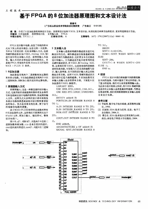
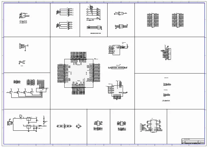
FPGA原理图
- 格式:pdf
- 大小:165.42 KB
- 文档页数:5

GW2A/GW2AR series of FPGA ProductsSchematic ManualIntroductionUsers should follow a series of rules during circuit board design when using the GW2A/GW2AR series of FPGA products. This manual describesthe characteristics and special features of GW2A/GW2AR series FPGAproducts and provides a comprehensive checklist to guide designprocesses. The main contents of this guide are as follows:●Power Supply●JTAG download●MSPI download●Clock pin●Difference pin●READY, RECONFIG_N, DONE●MODE●JTAGSEL_N●FASTRD_N●EXTR●Pin Multiplexing●Reference for the external crystal oscillator circuit●GW2AR Bank voltage●Supported configuration modes●Pin DistributionPower Supply1. OverviewVoltage types of the GW2A/GW2AR series of FPGA products include core voltage (V CC), PLL voltage (V CCPLL), auxiliary voltage (V CCX) and Bankvoltage (V CCIO).V CCX is an auxiliary power supply that is used to connect the internal part of the chip, with a 2.5V or 3.3V power supply. If no V CCX exists, I/O,OSC, and BSRAM circuits will be impacted and the chip will not befunctional.2. Power IndexUsers should ensure GOWINSEMI products are always used withinrecommended operating conditions and range. Data beyond the working conditions and range are for reference only. GOWINSEMI does notguarantee that all devices will operate as expected beyond the standard operating conditions and range.Table 1 lists the recommended working range for each power voltage.3. Total PowerFor specific density, packages, and resource utilization, GPA tools can be used to evaluate and analyze the power consumption.4. Power-on timeReference range of power-on time: 0.2 ms ~ 2 ms.Note!● If the power-on time is more than 2ms, you need to ensure that the power-on in sequence is V CC , and then V CCX /V CCIO ;●If the power-on time is less than 0.2ms, it is recommended to increase the capacitance to prolong the power-on time.5. Power FilterEach FPGA power input pin is connected to the ground with a 0.1uF ceramic capacitor.The input end of the V CC core voltage should primarily conduct the noise processing. Specific reference is as shown in Figure 1:Figure 1 Noise Processing of the Input End of the V CC Core VoltageGW2A/GW2AR series of FPGA products isolate and filter the V CCPLL . Specific reference is as shown in Figure 2:Figure 2 Isolate and Filter the V CCPLLFB is a magnetic bead, reference model mh2029-221Y , ceramic capacitance 4.7uF, 100nF and 10nF . It offers an accuracy of more than ±10%.JTAG Download1. OverviewJTAG download is used for downloading the bitstream data into the SRAM, on-chip flash or off-chip flash of the FPGA. 2. Signal Definition3. JTAG Circuit ReferenceFigure 3 JTAG Circuit ReferenceNote!● The resistance accuracy is not less than 5%;●The power supply of the 6th pin in the JTAG socket can be adjusted to VCC1P2, VCC1P5, VCC1P8 and VCC2P5 as required.MSPI Download1. OverviewAs a master device, the MSPI configuration mode reads theconfiguration data automatically from the off-chip flash and sends it to theFPGA SRAM.2. Signal Definition3. MSPI Circuit ReferenceFigure 4 MSPI Circuit ReferenceNote!The serial flash chip model is for reference only. Alternatively, serial flash storage with thesame index can be used. The resistance accuracy is not less than 5%.Clock Pin1. OverviewThe clock pins include GCLK global clock pins and PLL clock pins.GCLK: The GCLK pins in the GW2A/GW2AR series of FPGA products distribute in four quadrants. Each quadrant provides eight GCLK networks.The optional clock resources of the GCLK can be pins or CRU. Selectingthe clock from the dedicated I/Os can result in better timing.PLL: Frequency (multiply and division), phase, and duty cycle can be adjusted by configuring the parameters.2. Signal Definition3. Clock Input SelectionIf the external clock inputs as a PLL clock, the user is advised to input from the PLL dedicated pin. And the PLL_T end is selected if the externalclock inputs from the single-end.GCLK is the global clock and is directly connected to all resources in the device. The GCLK_T end is advised if the GCLK inputs from thesingle-end.Difference Pin1. OverviewDifferential transmission is a form of signal transmission technology that operates according to differences between the signal line and theground line. The differential transmit signals on these two lines, theamplitude of the two signals are equal and have the same phase butdemonstrate opposite polarity.2. LVDSLVDS is a low-voltage differential signal that offers low powerconsumption, low bit error rate, low crosstalk, and low radiation. Itfacilitates the transmission of data using a low-voltage swing high-speeddifferential. Different packages employ different signals. Please refer to theTrue LVDS section of the Package Pinout Manual for further details.Note!●All BANKs in the GW2A/GW2AR series of FPGA products support True LVDS output;●BANK0/1 in the GW2A/GW2AR series of FPGA products support 100 ohm differentialinput resistance;●If the BANK is used as the differential input, 100-ohm terminal resistance is needed;●The different line impedance of PCB is controlled at about 100 ohms. READY, RECONFIG_N, DONE1. OverviewRECONFIG_N is a reset function within the FPGA programming configuration. FPGA can't configure if RECONFIG_N is low.As a configuration pin, a low level signal with pulse width no less than 25ns is required to start GowinCONFIG to reload bitstream data accordingto the MODE setting value. You can control the pin via the write logic andtrigger the device to reconfigure.READY, the FPGA can configure only when the READY signal is high. The device should be restored by using the power on or triggering RECONFIG_N when the READY signal is low.As an output configuration pin, FPGA can be indicated for the current configuration state. If the device meets the configuration condition, READY signal is high. If the device fails to configure, the READY signal changes to low. As an input configuration pin, you can reduce the READY signal via its own logic or manually operate outside the device to delay configuration.DONE, the DONE signal indicates that the FPGA is configured successfully. The signal is high after successful configuration.As an output configuration pin, FPGA can be indicated whether the current configuration is successful. If configured successfully, DONE is high, and the device enters into a working state. If the device failed to configure, the DONE signal remains low. For the input type, the user can reduce the READY signal via its own internal logic or manually operate outside the device to delay progression to user mode.When the RECONFIG_N or READY signals is low. The DONE signal is low. DONE has no influence when SRAM is configuried through the JTAG circuit.2. Signal Definition3. Reference CircuitFigure 5 Reference CircuitNote!●The upper pull power supply is the bank voltage value of the corresponding pin;●The resistance accuracy is not less than ± 5%.MODE1. OverviewMODE spans the MODE0, MODE1, MODE2, and GowinCONFIG configuration MODE modes. When the FPGA powers on or a low pulsetriggers the RECONFIG_N mode, the device enters the correspondingGowinCONFIG state according to the MODE value. As the number of pinsfor each package is different, some MODE pins are not all packaged, andthe unpacked MODE pins are grounded inside. Please refer to thecorresponding PINOUT manual for further details.2. Signal Definition3. Mode SelectionJTAGSEL_N1. OverviewSelect the signal in JTAG mode. If the JTAG pin is set as GPIO in Gowin software, the JTAG pin is changed to GPIO pin after being poweredon and successfully configured. The JTAG pin can be recovered byreducing the JTAGSEL_N. The JTAG configuration functions are alwaysavailable if no JTAG pin multiplexing is set.2. Signal DefinitionNote!As GPIO, the JTAGSEL_N pin and the four pins (TCK, TMS, TDI, and TDO) configuredwith JTAG are mutual exclusive;●If JTAGSEL_N is set to GPIO, the JTAG pin can only be used as a configuration pin;●If JTAG is set to GPIO, the JTAGSEL_N pin can only be used as a configuration pin.FASTRD_N1. OverviewIn MSPI configuration mode, signals are selected via reading the SPI flash speed rate. FASTRD_N is normal read mode if high level; FASTRD_Nis high speed read mode if low level. Each manufacturer's flash high speedread instruction is different. Please refer to the corresponding flash datamanual.2. Signal DefinitionNote!In the high-speed flash access mode: the clock frequency is greater than 30MHz. EXTREXTR is a dedicated pin that needs to be connected to the ground with 10K resistance. The resistance precision is 1%.Specific reference is as shown in:Figure 6 EXTR Pin ConfigurationThe resistance accuracy is ±1%.Pin Multiplexing1. OverviewConfigure pin multiplexing refers to configuring during power-on, which is used as a normal I/O after downloading the bitstream file.Configure pin multiplex via the Gowin software:a). Open the corresponding project in Gowin software;b). Select “Project > Configuration > Dual Purpose Pin” from the menuoptions, as shown in Figure 7;c). Check the corresponding option to set the pin multiplex.Figure 8 Pin Multiplex2. Pin Multiplexing● SSPI: As a GPIO, SSPI can be used as input or output type;●MSPI: As a GPIO, MSPI can be used as input or output type; ● RECONFIG_N GPIO can only be used as an output type. Forsmooth configuration, set the initial value of RECONFIG_N as high when multiplexing it.●READY: As a GPIO, READY can be used as an input or output. Asan input GPIO for READY, the initial value of READY should be 1before configuring. Otherwise, the FPGA will fail to configure;●DONE: As a GPIO, DONE can be used as an input or output type.If DONE is used as an input GPIO, the initial value of DONE shouldbe 1 before configuring. Otherwise, the FPGA will fail to enter theuser mode after configuring;●JTAG: As a GPIO, JTAG can be used as an input or output type;●JTAGSEL_N: As a GPIO, JTAGSEL_N can be used as an input oroutput type.●DONE: As a GPIO, JTAG can be used as an input or output type. Inorder to smoothly configure, the user multiplexes the MODE pin,the correct configuration mode value is needed to provided duringconfiguration (power-on or low-level pulse triggers RECONFIG_N).Less than three pins can be multiplexed in the MODE. Unpackagedproducts are grounded internally. Please refer to PINOUT manualof the corresponding device for details. For the MODE valuecorresponding to different configuration modes, please refer to thecorresponding device configuration and programming manual.Note!If the Number of I/O ports are sufficient, use non-multiplexed pins first. FPGA External Crystal Oscillator Circuit ReferenceFigure 9 FPGA External Crystal Oscillator Circuitthan ±5% resistance accuracy, and more than ±10% capacitance accuracy.GW2AR Bank VoltageDue to the SIP SDRAM is in the GW2AR, the BANK voltage connected with it will have a fixed value, which is as follows:1. GW2AR-18 QN88 Package2. GW2AR-18 LQ144 Package3. GW2AR-18 LQ176 PackageSupported Configuration Modes1. GW2A-182. GW2A-553. GW2AR-18Pin DistributionBefore designing circuits, users should take the overall FPGA pin distribution needs into consideration and make informed decisions relatedto the application of the device architecture features, including I/O LOGIC,global clock resources, PLL resources, etc.All banks of the GW2A/GW2AR bank support true LVDS output. When using true LVDS output, V CCO shall be configured to 2.5 V or 3.3 V, andrefer to GW2A/GW2AR series FPGA Product Pinout to ensure that thecorresponding pins support true LVDS output.To support SSTL, HSTL, etc., each bank also provides oneindependent voltage source (V REF) as the reference voltage. Users canchoose V REF from the internal reference voltage of the bank (0.5 x VCCO)or external reference voltage V REF using any I/O from the bank.Support and FeedbackGowin Semiconductor provides customers with comprehensivetechnical support. If you have any questions, comments, or suggestions,please feel free to contact us directly using the information provided below.Website: E-mail: *********************Tel: 00 86 0755 ********Copyright©2018 Guangdong Gowin Semiconductor Corporation. All Rights Reserved.No part of this document may be reproduced or transmitted in any form or by any denotes, electronic, mechanical, photocopying, recording or otherwise, without the prior written consent of GOWINSEMI.DisclaimerGOWINSEMI®, LittleBee®, Arora™, and the GOWINSEMI logos are trademarks of GOWINSEMI and are registered in China, the U.S. Patent and Trademark Office and other countries. All other words and logos identified as trademarks or service marks are the property of their respective holders, as described at . GOWINSEMI assumes no liability and provides no warranty (either expressed or implied) and is not responsible for any damage incurred to your hardware, software, data, or property resulting from usage of the materials or intellectual property except as outlined in the GOWINSEMI Terms and Conditions of Sale. All information in this document should be treated as preliminary. GOWINSEMI may make changes to this document at any time without prior notice. Anyone relying on this documentation should contact GOWINSEMI for the current documentation and errata.Mouser ElectronicsAuthorized DistributorClick to View Pricing, Inventory, Delivery & Lifecycle Information:G OWIN Semiconductor:GW2A-LV18LQ144C8/I7GW2A-LV18PG256C7/I6GW2A-LV18PG256C8/I7GW2A-LV18PG484C7/I6GW2A-LV18PG484C8/I7GW2A-LV18EQ144C8/I7GW2A-LV55PG484C8/I7GW2A-LV55PG484C9/I8GW2A-LV55UG324C8/I7GW2A-LV18PG484C9/I8GW2A-LV18QN88A6GW2A-LV18QN88C7/I6GW2A-LV18QN88C8/I7 GW2A-LV18UG324C9/I8GW2A-LV55PG484A6GW2A-LV18MG196C8/I7GW2A-LV18PG256C9/I8GW2A-LV18PG256CC8/I7GW2A-LV18PG256CC9/I8GW2A-LV18PG256SC7/I6GW2A-LV18PG256SC8/I7。
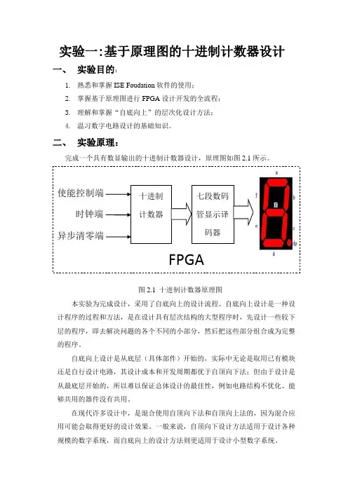
实验一:基于原理图的十进制计数器设计一、 实验目的:1. 熟悉和掌握ISE Foudation 软件的使用;2. 掌握基于原理图进行FPGA 设计开发的全流程;3. 理解和掌握“自底向上”的层次化设计方法;4. 温习数字电路设计的基础知识。
二、 实验原理:完成一个具有数显输出的十进制计数器设计,原理图如图2.1所示。
图2.1 十进制计数器原理图本实验为完成设计,采用了自底向上的设计流程。
自底向上设计是一种设计程序的过程和方法,是在设计具有层次结构的大型程序时,先设计一些较下层的程序,即去解决问题的各个不同的小部分,然后把这些部分组合成为完整的程序。
自底向上设计是从底层(具体部件)开始的,实际中无论是取用已有模块还是自行设计电路,其设计成本和开发周期都优于自顶向下法;但由于设计是从最底层开始的,所以难以保证总体设计的最佳性,例如电路结构不优化、能够共用的器件没有共用。
在现代许多设计中,是混合使用自顶向下法和自顶向上法的,因为混合应用可能会取得更好的设计效果。
一般来说,自顶向下设计方法适用于设计各种规模的数字系统,而自底向上的设计方法则更适用于设计小型数字系统。
十进制计数器七段数码管显示译码器使能控制端时钟端 异步清零端FPGA1、七段数码管译码器的设计七段数码管属于数码管的一种,是由7段二极管组成。
按发光二极管单元衔接方式分为共阳极数码管和共阴极数码管。
本实验使用共阴数码管。
它是指将一切发光二极管的阴极接到一同构成公共阴极(COM)的数码管。
共阴数码管在应用时应将公共极COM接到地线GND上,当某一字段发光二极管的阳极为高电平相应字段就点亮,当某一字段的阳极为低电平相应字段就不亮。
显示译码器,一般是将一种编码译成十进制码或特定的编码,并通过显示器件将译码器的状态显示出来。
根据显示的要求,可以得到七段显示译码器产生的各段LED输出与输入的二进制对应关系:表2.1七段字符显示真值表最小项译码器输出能产生输入变量的所有最小项,而任何一个组合逻辑函数都可以变换为最小项之和的标准形式,故采用译码器和门电路可实现任何单输出或多输出的组合逻辑函数。

F PG A原理图方式设计流程Revised by Petrel at 20212Q u a r t u s I I软件的使用、开发板的使用本章将通过3个完整的例子,一步一步的手把手的方式完成设计。
完成这3个设计,并得到正确的结果,将会快速、有效的掌握在AlteraQuartusII软件环境下进行FPGA设计与开发的方法、流程,并熟悉开发板的使用。
2.1原理图方式设计3-8译码器一、设计目的1、通过设计一个3-8译码器,掌握祝组合逻辑电路设计的方法。
2、初步了解QuartusII采用原理图方式进行设计的流程。
3、初步掌握FPGA开发的流程以及基本的设计方法、基本的仿真分析方法。
二、设计原理三、设计内容四、设计步骤1、建立工程文件1)双击桌面上的QuartusII的图标运行此软件。
开始界面2)选择File下拉菜单中的NewProjectWizard,新建一个工程。
如图所示。
新建工程向导3)点击图中的next进入工作目录。
新建工程对话框4)第一个输入框为工程目录输入框,用来指定工程存放路径,建议可根据自己需要更改路径,若直接使用默认路径,可能造成默认目录下存放多个工程文件影响自己的设计,本步骤结束后系统会有提示(当然你可不必理会,不会出现错误的)。
第二个输入框为工程名称输入框。
第三个输入框为顶层实体名称输入框,一般情况下保证工程名称与顶层实体名称相同。
设定完成后点击next。
指定工程路径、名称5)设计中需要包含的其它设计文件,在此对话框中不做任何修改,直接点击next。
工程所需其它文件对话框6)在弹出的对话框中进行器件的选择。
在DeviceFamily框中选用CycloneII,然后在Availabledevice框中选择EP2C35F484C8,点击next进入下一步。
器件选择界面7)下面的对话框提示可以勾选其它的第三方EDA设计、仿真的工具,暂时不作任何选择,在对话框中按默认选项,点击next。

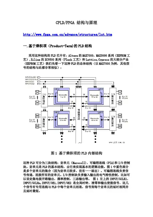
CPLD/FPGA 结构与原理/advance/structures/lut.htm一.基于乘积项(Product-Term)的PLD结构采用这种结构的PLD芯片有:Altera的MAX7000,MAX3000系列(EEPROM工艺),Xilinx的XC9500系列(Flash工艺)和Lattice,Cypress的大部分产品(EEPROM工艺)我们先看一下这种PLD的总体结构(以MAX7000为例,其他型号的结构与此都非常相似):图1 基于乘积项的PLD内部结构这种PLD可分为三块结构:宏单元(Marocell),可编程连线(PIA)和I/O控制块。
宏单元是PLD的基本结构,由它来实现基本的逻辑功能。
图1中蓝色部分是多个宏单元的集合(因为宏单元较多,没有一一画出)。
可编程连线负责信号传递,连接所有的宏单元。
I/O控制块负责输入输出的电气特性控制,比如可以设定集电极开路输出,摆率控制,三态输出等。
图1 左上的INPUT/GCLK1,INPUT/GCLRn,INPUT/OE1,INPUT/OE2 是全局时钟,清零和输出使能信号,这几个信号有专用连线与PLD中每个宏单元相连,信号到每个宏单元的延时相同并且延时最短。
宏单元的具体结构见下图:图2 宏单元结构左侧是乘积项阵列,实际就是一个与或阵列,每一个交叉点都是一个可编程熔丝,如果导通就是实现“与”逻辑。
后面的乘积项选择矩阵是一个“或”阵列。
两者一起完成组合逻辑。
图右侧是一个可编程D触发器,它的时钟,清零输入都可以编程选择,可以使用专用的全局清零和全局时钟,也可以使用内部逻辑(乘积项阵列)产生的时钟和清零。
如果不需要触发器,也可以将此触发器旁路,信号直接输给PIA或输出到I/O脚。
二.乘积项结构PLD的逻辑实现原理下面我们以一个简单的电路为例,具体说明PLD是如何利用以上结构实现逻辑的,电路如下图:图3假设组合逻辑的输出(AND3的输出)为f,则f=(A+B)*C*(!D)=A*C*!D + B*C*!D ( 我们以!D表示D的“非”)PLD将以下面的方式来实现组合逻辑f:图4A,B,C,D由PLD芯片的管脚输入后进入可编程连线阵列(PIA),在内部会产生A,A反,B,B反,C,C反,D,D反8个输出。
GW2A/GW2AR系列FPGA产品原理图指导手册简介使用高云半导体GW2A/GW2AR系列FPGA产品做电路板设计时需遵循一系列规则。
本文档详细描述了GW2A/GW2AR系列FPGA产品相关的一些器件特性和特殊用法,并给出校对表用于指导原理图设计,主要内容如下:●电源●JTAG下载●MSPI下载●时钟管脚●差分管脚●READY、RECONFIG_N、DONE●MODE●JTAGSEL_N●FASTRD_N●EXTR●配置管脚复用●外接晶振电路参考●GW2AR Bank电压●各器件支持的配置模式●管脚分配电源1.概述GW2A/GW2AR系列FPGA产品电压种类包括V CC核电压、V CCPLL锁相环电压、V CCX辅助电压和V CCIO Bank电压。
V CCX为辅助电源,用于给芯片内部部分电路供电,需要接2.5V或者3.3V 电压,如果V CCX电压不接,会影响IO、OSC、BSRAM等电路工作,造成芯片无法使用。
2.电源指标建议在推荐的工作条件及工作范围内使用高云器件,超出工作条件及工作范围的数据仅供参考,高云半导体不保证所有器件都能在超出工作条件及工作范围的情况下正常工作。
表1列出了各电源电压的推荐工作范围。
3.总体功耗针对特定密度、封装和资源利用率,可以使用云源软件内嵌的GPA工具进行功耗评估和分析。
4.上电时间电源上电时间参考范围值:0.2ms ~2ms。
注!●如果上电时间>2ms,则需要确保上电顺序为先V CC,后V CCX/V CCIO;●如果上电时间<0.2ms,建议增加电容以延长上电时间。
5.电源滤波每一个FPGA电源输入脚就近连接一个0.1uF陶瓷电容到地;对于VCC核电压输入端要重点进行噪声处理,具体参考如图1所示:图 1 VCC核电压输入端噪声处理V1P0VCCFBC4.7uFGW2A/GW2AR系列FPGA产品需要对V CCPLL隔离滤波,具体参考如图2所示:图2隔离滤波V CCPLLV1P0VCCPLLFBC4.7uF C C 100nF10nF其中FB为磁珠,参考型号MH2029-221Y,4.7uF、100nF、10nF均为陶瓷电容,精度不低于±10%。