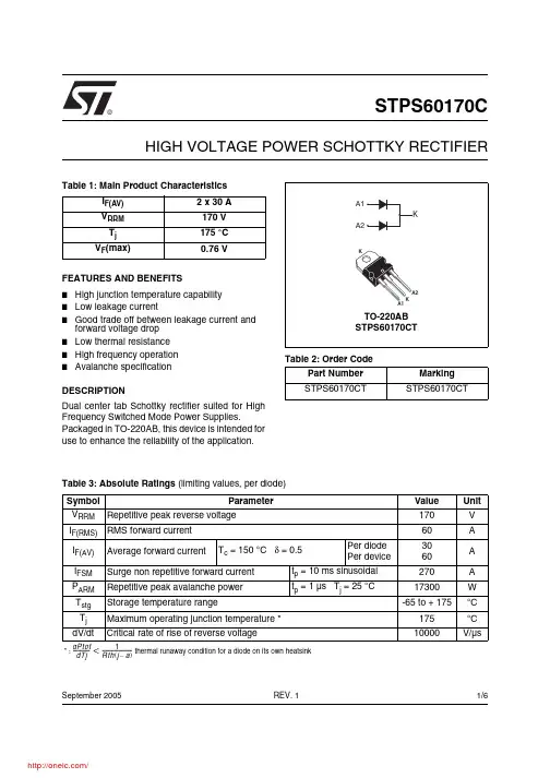
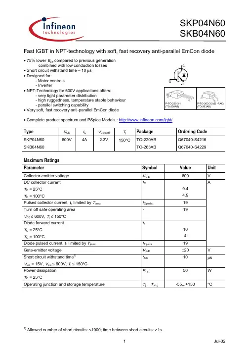
STP4NM60中文资料
- 格式:pdf
- 大小:552.39 KB
- 文档页数:12
1/12September 2002STP4NM60STD3NM60 - STD3NM60-1N-CHANNEL 600V - 1.3Ω - 3A TO-220/DPAK/IPAKZener-Protected MDmesh™Power MOSFETs TYPICAL R DS (on) = 1.3 Ωs HIGH dv/dt AND AVALANCHE CAPABILITIES s IMPROVED ESD CAPABILITYsLOW INPUT CAPACITANCE AND GATE CHARGEs LOW GATE INPUT RESISTANCEsTIGHT PROCESS CONTROL AND HIGH MANUFACTORING YIELDSDESCRIPTIONThe MDmesh ™ is a new revolutionary MOSFET technology that associates the Multiple Drain pro-cess with the Company’s PowerMESH™ horizontal layout. The resulting product has an outstanding low on-resistance, impressively high dv/dt and excellent avalanche characteristics. The adoption of the Company’s proprietary strip technique yields overall dynamic performance that is significantly better than that of similar completition’s products.APPLICATIONSThe MDmesh™ family is very suitable for increase the power density of high voltage converters allow-ing system miniaturization and higher efficiencies.ORDERING INFORMATIONTYPE V DSS R DS(on)I D Pw STP4NM60STD3NM60STD3NM60-1600 V 600 V 600 V< 1.5 Ω< 1.5 Ω< 1.5 Ω4 A 3 A 3 A69 W 42 W 42 WSALES TYPE MARKING PACKAGE PACKAGINGSTP4NM60P4NM60TO-220TUBE STD3NM60T4D3NM60DPAK TAPE & REELSTD3NM60-1D3NM60IPAKTUBESTP4NM60 / STD3NM60 / STD3NM60-12/12ABSOLUTE MAXIMUM RATINGS(l ) Pulse width limited by safe operating area(1) I SD ≤3A, di/dt ≤400 µA, V DD ≤ V (BR)DSS , T j ≤ T JMAX.THERMAL DATAAVALANCHE CHARACTERISTICSGATE-SOURCE ZENER DIODEPROTECTION FEATURES OF GATE-TO-SOURCE ZENER DIODESThe built-in back-to-back Zener diodes have specifically been designed to enhance not only the device’s ESD capability, but also to make them safely absorb possible voltage transients that may occasionally be applied from gate to source. In this respect the Zener voltage is appropriate to achieve an efficient and cost-effective intervention to protect the device’s integrity. These integrated Zener diodes thus avoid the usage of external components.SymbolParameterValueUnitSTP4NM60STD3NM60STD3NM60-1V DS Drain-source Voltage (V GS = 0)600V V DGR Drain-gate Voltage (R GS = 20 k Ω)600V V GS Gate- source Voltage± 30V I D Drain Current (continuous) at T C = 25°C 43A I D Drain Current (continuous) at T C = 100°C 2.52 1.9A I DM (l )Drain Current (pulsed)1612A P TOT Total Dissipation at T C = 25°C 6942W Derating Factor0.550.33W/°C dv/dt (1)Peak Diode Recovery voltage slope 15V/ns T j T stgOperating Junction Temperature Storage Temperature-65 to 150-65 to 150°C °CTO-220DPAK IPAK Rthj-case Thermal Resistance Junction-case Max 1.823°C/W Rthj-ambThermal Resistance Junction-ambient Max62.5°C/W T lMaximum Lead Temperature For Soldering Purpose300°CSymbol ParameterMax ValueUnit I AR Avalanche Current, Repetitive or Not-Repetitive (pulse width limited by T j max)1.5A E ASSingle Pulse Avalanche Energy(starting T j = 25 °C, I D = I AR , V DD = 50 V)200mJSymbol ParameterTest ConditionsMin.Typ.Max.Unit BV GSOGate-Source Breakdown VoltageIgs=± 1mA (Open Drain)30V3/12STP4NM60 / STD3NM60 / STD3NM60-1ELECTRICAL CHARACTERISTICS (T CASE =25°C UNLESS OTHERWISE SPECIFIED)ON/OFFDYNAMICSWITCHING ONSWITCHING OFFSOURCE DRAIN DIODENote: 1.Pulsed: Pulse duration = 300 µs, duty cycle 1.5 %.2.Pulse width limited by safe operating area.Symbol ParameterTest ConditionsMin.Typ.Max.Unit V (BR)DSS Drain-sourceBreakdown Voltage I D = 250 µA, V GS = 0600V I DSS Zero Gate VoltageDrain Current (V GS = 0)V DS = Max RatingV DS = Max Rating, T C = 125 °C 110µA µA I GSS Gate-body Leakage Current (V DS = 0)V GS = ± 20V±5µA V GS(th)Gate Threshold Voltage V DS = V GS , I D = 250µA 345V R DS(on)Static Drain-source On ResistanceV GS = 10V, I D = 1.5 A1.31.5ΩSymbol ParameterTest ConditionsMin.Typ.Max.Unit g fs (1)Forward Transconductance V DS = 15 V , I D =1.5 A 2.7S C iss C oss C rssInput Capacitance Output Capacitance Reverse Transfer CapacitanceV DS = 25V, f = 1 MHz, V GS = 03241327.4pF pF pFSymbol ParameterTest ConditionsMin.Typ.Max.Unit t d(on)t r Turn-on Delay Time Rise TimeV DD = 300 V, I D = 1.5 A R G =4.7Ω V GS = 10 V(Resistive Load see, Figure 3)94ns ns Q g Q gs Q gdTotal Gate Charge Gate-Source Charge Gate-Drain ChargeV DD = 480V, I D = 3 A,V GS = 10V1034.714nC nC nCSymbol ParameterTest ConditionsMin.Typ.Max.Unit t r(Voff)t f t cOff-voltage Rise Time Fall TimeCross-over TimeV DD = 480 V, I D = 3 A, R G =4.7Ω, V GS = 10V(Inductive Load see, Figure 5)16.510.515ns ns nsSymbol ParameterTest ConditionsMin.Typ.Max.Unit I SD I SDM (2)Source-drain CurrentSource-drain Current (pulsed)312A A V SD (1)Forward On Voltage I SD = 3 A, V GS = 0 1.5V t rr Q rr I RRM Reverse Recovery Time Reverse Recovery Charge Reverse Recovery Current I SD = 3 A, di/dt = 100A/µs V DD = 100 V, T j = 25°C (see test circuit, Figure 5)22419ns µC A t rr Q rr I RRMReverse Recovery Time Reverse Recovery Charge Reverse Recovery CurrentI SD = 3 A, di/dt = 100A/µs V DD = 100 V, T j = 150°C (see test circuit, Figure 5)2961.49.3ns µC ASTP4NM60 / STD3NM60 / STD3NM60-14/12Output Characteristics5/12STP4NM60 / STD3NM60 / STD3NM60-1STP4NM60 / STD3NM60 / STD3NM60-1 Source-drain Diode Forward Characteristics6/127/12STP4NM60 / STD3NM60 / STD3NM60-1Fig. 5: Test Circuit For Inductive Load Switching And Diode Recovery TimesFig. 4: Gate Charge test CircuitFig. 2: Unclamped Inductive WaveformFig. 1:Unclamped Inductive Load Test CircuitFig. 3: Switching Times Test Circuit ForResistive LoadSTP4NM60 / STD3NM60 / STD3NM60-18/12STP4NM60 / STD3NM60 / STD3NM60-19/12STP4NM60 / STD3NM60 / STD3NM60-110/1211/12STP4NM60 / STD3NM60 / STD3NM60-1TAPE AND REEL SHIPMENT (suffix ”T4”)*TUBE SHIPMENT (no suffix)*DPAK FOOTPRINT * on sales typeDIM.mm inch MIN.MAX.MIN.MAX.A 33012.992B 1.50.059C 12.813.20.5040.520D 20.20.795G 16.418.40.6450.724N 501.968T22.40.881BASE QTY BULK QTY 25002500REEL MECHANICAL DATADIM.mm inch MIN.MAX.MIN.MAX.A0 6.870.2670.275B010.410.60.4090.417B112.10.476D 1.5 1.60.0590.063D1 1.50.059E 1.65 1.850.0650.073F 7.47.60.2910.299K0 2.55 2.750.1000.108P0 3.9 4.10.1530.161P17.98.10.3110.319P2 1.9 2.10.0750.082R 40 1.574W15.716.30.6180.641TAPE MECHANICAL DATAAll dimensions are in millimetersAll dimensions are in millimetersSTP4NM60 / STD3NM60 / STD3NM60-112/12Information furnished is believed to be accurate and reliable. However, STMicroelectronics assumes no responsibility for the consequences of use of such information nor for any infringement of patents or other rights of third parties which may result from its use. No license is granted by implication or otherwise under any patent or patent rights of STMicroelectronics. Specifications mentioned in this publication are subject to change without notice. This publication supersedes and replaces all information previously supplied. STMicroelectronics products are not authorized for use as critical components in life support devices or systems without express written approval of STMicroelectronics.© The ST logo is a registered trademark of STMicroelectronics© 2002 STMicroelectronics - Printed in Italy - All Rights ReservedSTMicroelectronics GROUP OF COMPANIESAustralia - Brazil - Canada - China - Finland - France - Germany - Hong Kong - India - Israel - Italy - Japan - Malaysia - Malta - Morocco Singapore - Spain - Sweden - Switzerland - United Kingdom - United States.© 。