ks8995_以太网交换芯片
- 格式:pdf
- 大小:43.46 KB
- 文档页数:2

⽹卡驱动⼀、配置菜单Device Drivers[*] Network device support --->⽹络设备驱动、⽹卡驱动< > Bonding driver support功能:多⽹卡绑定具体操作为:将多个以太⽹通道绑定为⼀个,也就是两块⽹卡具有相同的IP地址并且聚合成⼀个逻辑链路⼯作,可以⽤来实现负载均衡或硬件冗余< > Dummy net driver support功能:哑接⼝⽹络使⽤环境:使⽤SLIP或PPP传输协议(如ADSL⽤户)的需要它具体操作:设置⼀个虚拟⽹络。
虚拟⽹络(dummy network)就像⽹络中的/dev/null。
任何发送给虚拟⽹络的数据都会永久消失,因为它会发往/dev/null。
IP地址没有设置。
⽤户可以定义他们的⽹络相当于/dev/null)< > EQL (serial line load balancing) support功能:串⾏线路的负载均衡具体操作:如果有两个MODEM和两条电话线⽽且⽤SLIP或PPP协议,该选项可以让您同时使⽤这两个MODEM以达到双倍速度(在⽹络的另⼀端也要有同样的设备)< > Generic Media Independent Interface device support功能:通⽤媒体独⽴接⼝设备⽀持背景介绍:MII是⼀种⽤于最⾼速度为100Mbit/s以太⽹的接⼝。
以太⽹线缆⽤于连接到PHY ceiver,是⼀种以太⽹收发器< > Ethernet team driver support (EXPERIMENTAL) --->功能:team⽹卡组⽀持背景介绍:通过虚拟接⼝组织许多以太⽹设备< > MAC-VLAN support (EXPERIMENTAL)功能:允许⽤户在特定的MAC地址和某个接⼝上映射数据包具体操作:基于MAC地址的VLAN,⼀种根据报⽂的源MAC地址来确定untagged报⽂所属VLAN的划分⽅法< > Network console logging support⽹络远程命令⽀持,远程登录⽤注意:内核发送给⽹络的消息可任意通过这个特性记录下来。

KS8995芯片VLAN技术分析一、市场需求目前已经明确的4口光纤收发器应用场景有两种,后续可能还有其他的应用场景的需求。
一种就是光口上行接到MSAP或者交换机设备,4个电口接入4台监控设备,4个电口物理隔离。
一种就是光口上行接到MSAP或者交换机设备,而4个电口接入不同部门或公司的业务,不同部门或公司的业务需要隔离。
针对4口光纤收发器的应用场景,结合KS8995芯片实现,对KS8995芯片的VLAN技术从以下几个方面进行分析:交换模式:透传模式和VLAN模式端口类型:Access、Trunk和Hybrid端口PVID:端口默认VLANVLAN表项:端口加入VLAN并且下发硬件端口隔离:端口物理隔离功能VLAN-VPN:芯片不支持。
二、实现方法1.交换模式KS8995芯片默认交换模式为透传模式(Global Control 3(Reg0x05)的BIT7设置0),光纤收发器的端口不识别报文中带的VLAN tag,报文查找MAC转发表进行转发。
KS8995芯片另外一种模式就是VLAN模式(Global Control 3(Reg0x05)的BIT7设置1),光纤收发器的端口需要识别报文中带的VLAN tag。
如果报文中带VLAN tag,则报文的VLAN 指定该VLAN tag的VID;如果报文中不带VLAN tag,则报文的VLAN指定该端口的默认VLAN (PVID)。
然后根据VLAN查找VLAN表中获取FID,通过FID+MAC查找MAC转发表进行转发。
2.端口隔离通过端口隔离特性,用户可以对需要进行控制的端口配置端口隔离功能,实现所有需要隔离端口之间业务数据的隔离,既增强了网络的安全性,也为用户提供了灵活的组网方案。
此功能可以通过配置寄存器(Port N Control 1的BIT0~4)来实现。
例如要实现P1、P2的隔离,只需将P1的BIT1清零(即0x1d)、P2的BIT0清零(即0x1e)。
88E6095在电力以太网交换机的应用作者:马晓军莫非来源:《电子世界》2012年第14期【摘要】本文介绍了88E6095芯片在电力以太网交换机的设计应用,介绍了电力以太网交换机的特点,详细阐述了一款电力以太网交换机的软硬件设计。
本设计的突出特点是安全可靠,有诊断跟自恢复的能力,满足电力系统的通信要求。
【关键词】88E6095;电力以太网交换机;电力系统一、电力以太网交换机概述电力专用工业以太网交换机是面向智能变电站应用而开发的高性能、高可靠和高安全的工业级网络交换设备。
它充分考虑了变电站的严酷工作环境和网络通信需求,采用了电信级以太网、硬件时间戳、QoS、智能内容识别等先进技术,使得智能变电站通信系统更加可靠;能有效地抵御DOS攻击,保证GOOSE报文优先转发,实现网络时间精确同步。
二、88E6095芯片介绍88E6095是Marvell公司设计的一款网络交换芯片。
该芯片集成了MAC和PHY,有11个端口,可以提供三个千兆的以太网网口和8个百兆的以太网网口,时钟源频率25MHz。
其中P0~P7,8个端口支持10BAST-T/100 BAST-T;P8、P9、P10端口都支持三种接口:SEDES接收器、外接10/100/1000M Copper PHYS、1000BASE-X的光纤端口,能够直接连接到光放大器。
另外,P9还支持MII-MAC/PHY,P10还支持(G)MII-MAC/PHY。
该芯片支持VLAN、STP生成树协议和QoS。
三、设计思路1.采用4片88E6095F芯片进行互连,完成交换功能。
2.每个芯片上的3个Serdes千兆端口都是两两互联的。
3.为了避免成环,默认开启88E6095的24P模式(级联模式)。
4.交换机由AMR9 CPU进行管理。
四、具体实现1.电源采用12V稳压电源供电,经过LM1085-5.0电源转换芯片输出5V的稳压电源,再经过3块电源转换芯片FAN2106分别输出3.3V、2.5V和1.2V的电压用来给交换芯片88E6095和其他部件供电。

NW604不明牌子400WIFI模块应用领域:串口(RS232/RS485)转WiFi、SPI转WiFi;WiFi远程控制/监控、TCP/IP和Wi-Fi协处理器;WiFi遥控飞机、车等玩具领域;WiFi网络收音机、摄像头、数码相框;医疗仪器、数据采集、手持设备;WiFi脂肪秤、智能卡终端;家居智能化;LED照明灯具电源开关仪器仪表、设备参数监测、无线POS机;现代农业、军事领域等其他无线相关二次开发应用。
汽车电子智能电网工业控制NO中文名称型号方案flash(M)DDR(M)Data Rate(速率)(M)RF Power壳料材质Power(optional)(源)1CPE cpe00793418M/16M 32/64M300B:28±2,N:胶壳18V/1A 2CPE cpe00893448M/16M64/128M300500MW胶壳18V/1A 3CPE cpe01293318M/16M 32/64M150500MW胶壳18V/1A 4CPE cpe0177240+92858M/16M 32/64M150100MW胶壳18V/1A 5CPE cpe0207240+92858M/16M 32/64M150100MW胶壳18V/1A 6CPE cpe0217240+92838M/16M 32/64M300500MW胶壳18V/1A 7CPE/壁挂APcpe0217240+92838M/16M 32/64M300500MW铁壳18V/1A 8CPE/壁挂APAP023934416M 128M300500MW铁壳18V/1A9CPE/壁挂AP SX-AP-23A AR934416M64M/128Mdual-frequency/B:23±2A:22±2铁壳10CPE/壁挂APAR93418M/16M 64M300500MW铁壳24V POEor48V POE 11CPE/壁挂APSX-AP-23A AR934416M128M600300铁壳24V POEor48V POE12CPE/壁挂AP SX-AP-23A AR934416M64M/128Mdual-frequency/B:23±2A:22±2铁壳13入墙AP SX-RQAP-01B AR93318M/16M 32/64M150100MW胶壳POE04BorPOE15Aor 14入墙AP SX--RQAP-05A AR93418M/16M 32/64M300B:18±胶壳POE08A15入墙AP SX-rqap_07A AR93418M64M300300MW胶壳POE04BorPOE15A 16室外AP SX-AP-03AR934416M128Mdual-frequency600M/B:27±铁壳POE06BA:24/2617吸顶AP SX-AP-10A6 AR93418M/16M 32/64M300B:28±2胶壳dual-frequencyB:27±2,n:2018吸顶AP SX-AP-15B AR934416M128M胶壳600M/A:22±2,n:20胶壳19吸顶AP SX-AP159344+938216M128M300M/B:27±2,n:2020吸顶AP SX-AP-16A AR93318M/16M 32/64M150500MW胶壳21吸顶AP SX-AP1981978M/16M 32/64M600M200MW(23DBM)胶壳POE06B/22吸顶AP SX-AP-20A8192+81968M/16M 32/64M300M500MV胶壳POE06B/23吸顶AP SX-AP-21A8197DL8M/16M 32/64M600Mbps200mW胶壳POE06B/POE06B/POE12A/24吸顶AP SX-AP-22A1AR93418M/16M 32/64M300B:28±2,N:胶壳(falsePOE 24V1A)25路由LY-03C93418M/16M 64M300Mbps500mW胶壳26路由LY-06B AR93448M/16M 64M/128M300Mbps500mW胶壳MTK7620N27路由LY-08A8M64M300Mbps100mW胶壳A128路由LY-09A AR93418M64M300Mbps200mW胶壳29路由LY-10A MTK7620A8M/16M 64M/128M300Mbps500mW胶壳30路由LY-10B MTK7620A8M/16M 64M/128M dual-frequency 300Mbps500mW铁壳31路由RT-03C93418/16M64M300Mbps500mW铁壳32路由RT-06B AR93448/16M64/128M300Mbps500mW铁壳33模块SX-9331MK-01A AR93318M/16M 32M/64M15050MW34模块AR9331-PCB-A293318M/16M 32M/64M15050MW35模块SX-9331MK-04A AR93318M/16M 32M/64M15050MWdual-frequency36模块MK-06A AR93448M/16M64M/128M50MW300M/37模块SX-9331MK-07A AR93318M/16M 32M/64M38模块SX-9331MK-08A A R933116M64M15050MW39模块SX-9331MK-11A AR93318M/16M 32/64M15050MW40模块SX-9331MK-12A AR93318M/16M 32/64M15050MW41模块SX-9331MK-13A AR93318M/16M 32/64M15050MW42模块SX-MK-15A93418M/16M 32/64M300B:23±243模块SX-AP9331-CPU93318M/16M 32/64M15050MW44模块SX-9331MK-20A93318M/16M 32/64M15050MW45模块SX-9331MK-21A93318M/16M 32/64M46网卡SHX007C AR9220NO NO300300MW47网卡SHX002D AR9223NO NO300500MW48网卡MB92网卡NO NO300500MW49网卡SHX22A9382NO NO300A:21±50网卡SHX22A1AR9382NO NO300A:21±51网卡SHX023A8192NO NO300100MW本文由于作者精力与能力所限,所列型号大部分只能为国产,或YLJ+水货,且也不能列举所有型号和所有版本,但阅读完本文应该已能辨别绝大部分路由的好坏本文如有疏漏,也请各位不吝指正另,路由猫不在本文讨论范围内基本知识储备:1.关键词:解决方案路由厂家实在太多,但是能生产路由主芯片的厂家则很少,路由厂你可以理解为主板厂,而提供无线和主芯片的厂家则可对应理解为intel 和 AMD,后者提供解决方案,前者则生产出最终的路由成品卖到消费者手中,如下图所示Athros的官方解决方案:AR9001AP-2NG(AR9130+AR9102+AR)和 d-link,TP-link对应的自己的出场成品(后者可能处于成本或者性能考虑,交换芯片更换成Marvell的产品)Athers官方解决方案:AP81图片来自: alan_rei的百度相册d-link dir615 c1版TP-link 841n v3版(交换芯片更改成 Marvell 88E6060,性能没有区别)现在无线路由的解决方案主要由两大厂家把持——Broadcom(博通)和Atheros(目前已被Qualcomm高通收购) 以下是两家的产品列表链接:Atheros wiki/AtherosAtheros被收购后设计的芯片wiki/Qualcomm_AtherosBroadcom wiki/Broadcom!!这两家的解决方案将是重点,图例和说明在下一楼上!!还有少部分份额则是由廉价的螃蟹(realtek),Ralink(雷凌)和比较昂贵(还是没有Broadcom贵,博通方案,特别是高端解决方案纯属于坑爹价的类型)的Marvell,Ubicom(只用主芯片的解决方案,没有无线芯片的解决方案,D-link的中高端产品用的最多)方案占据.(早期的主芯片解决方案中还有intel的strongARM插足,如有名的IXP4XX系类)D-link dir-655 A3版解决方案:主芯片Ubicom IP5160U,千兆交换芯片VITESSE VSC7385,无线基带+射频芯片:Atheros AR5416+AR2133(MINI PCI)Ubicom属于比较小众的解决方案,但却是D-link的御用芯片,这种芯片的特点是多线程的性能非常好,这也是D-link 一直再上默默投入的原因,D-link很早就在此基础上开发了自己流控固件,类似于killer网卡的那种QOS,可以设置网络游戏封包的优先权,高端系列的转发也很不错,无线方面一般是配合Atheros的无线网卡,所以无线性能也很有保障,缺点嘛,显而易见,芯片集成度不高,整套方案很繁杂,成本很高belkin 8235-4 V2 (v2000)解决方案:主芯片+无线 Ralink RT3025F ,千兆交换芯片 realtek RTL8366RB/SB其实Ralink的这个芯片已经集成了一个百兆的交换机,只是这个路由需要千兆的功能所以外加了千兆的交换芯片,Ralink的解决方案一般集成度比较高,也比较廉价,但是 Ralink的由于无线和网络芯片的研发起步的比较早,所以性能还是很不错的,不过产品线比较单一,优势是在信号和传输稳定上,缺点则是芯片的发热(集成度高)和的极限传输速度上代表产品还有 MOTO 2108-N9/D9 , ASUS RT-N13, 华为HG255Ddir 615 A版解决方案:主芯片Marvell 88F5180, 交换芯片Marvell 88E6061, 无线基带+射频芯片 Marvell 88W8361P+88W8060可以看出 Marvell的方案一般为全套的解决方案,一般不会与其他芯片混用,而且设计的也比较复杂,成本比较高,典型代表还有 Netgear的WNR854T和苹果的airport extreme base station A1354,优点是无线极限传输性能不错,主芯片转发也不错,缺点是方案复杂,成本很高dir-615 F3版或FG版解决方案:主芯片+无线芯片+交换芯片 Realtek RTL8196B廉价路由上用烂的方案,性能不是很好,不管是转发抑或是无线覆盖或是传输稳定性,口碑都不好,FG版也成为国内 615系列口碑最烂的版本,Realtek做无线相对较少,对这方面投入的没有有线那么多,54M的时候很响亮的 8187L USB无线网卡解决方案是其经典的代表作,但是近几年的在无线方面建树较少,所以无线路由选购时尽量不要选采用螃蟹芯片的产品linksys WRV54G V1解决方案:主芯片 intel IXP425 @266MHz,交换芯片KENDIN KS8995M, 无线基带+射频芯片Intersil ISL3880 +ISL3686A,自从Intel将 strongARM卖给Marvell以后, Intel的解决方案自此从路由市场销声匿迹了,这是04年初上市的老路由,一般Intel解决方案都定位为中小企业及的产品,比家用级高一个档次,这款型号对应的家用版本就是赫赫有名的WRT54G,但显然IXP425的性能是Broadcom BCM4712这类芯片所不能比拟的,所以也注定了他的过高的身价,在市场中的产品也是凤毛麟角,代表产品还有Actiontec MI424WR(此款为IXP425全频版 @533MHz ), linksys WRT300N v1,casio RV042注释:进入无线时代,主要的无线芯片厂都拿出了自己解决方案Broadcom叫INTENSI-FI,Atheros 叫XSPAN,Marvell叫Top Dog,螃蟹和雷凌的叫法不详2.各路由厂家的喜好linksys(Casio):intel(早期),BroadcomASUS:BroadcomNetgear:Broadcom,Marvell(中高端),Atheros(中低端),Realtek(低端)Buffalo:Broacom( 早期),Atheros(目前,高端),Ralink(目前,低端)apple:Marvell+Atheros(前者提供主芯片,后者提供无线)Belkin: Broadcom(中高端),Ralink(中低端)d-link:Ubicon+Atheros(中高端:前者提供主芯片,后者提供无线),Atheros(中低端),Ralink(中低端),Marvell(中端),realtek(低端)moto:Broadcom,RalinkTPlink&Mercury&FAST(普联,水星,迅捷基本算是一家公司):Atheros, MTK(是的你没看错)以上是比较常见的牌子,韩国棒子的ToTolink和斐讯国内也有一定市场,但是我没玩过,所以就不说了。
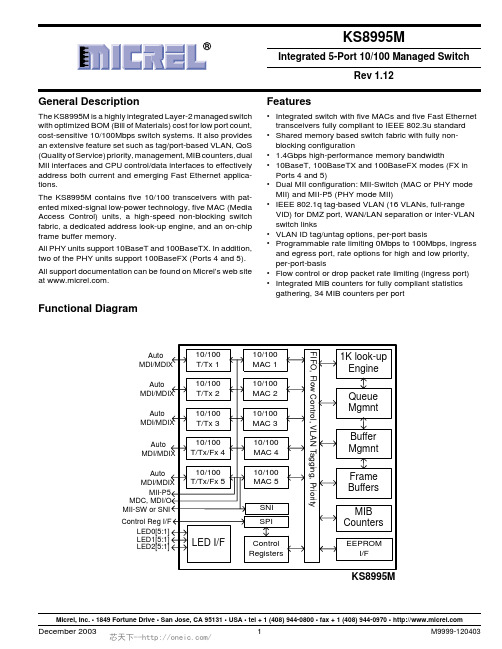
General DescriptionThe KS8995M is a highly integrated Layer-2 managed switch with optimized BOM (Bill of Materials) cost for low port count,cost-sensitive 10/100Mbps switch systems. It also provides an extensive feature set such as tag/port-based VLAN, QoS (Quality of Service) priority, management, MIB counters, dual MII interfaces and CPU control/data interfaces to effectively address both current and emerging Fast Ethernet applica-tions.The KS8995M contains five 10/100 transceivers with pat-ented mixed-signal low-power technology, five MAC (Media Access Control) units, a high-speed non-blocking switch fabric, a dedicated address look-up engine, and an on-chip frame buffer memory.All PHY units support 10BaseT and 100BaseTX. In addition,two of the PHY units support 100BaseFX (Ports 4 and 5).All support documentation can be found on Micrel’s web site at .Features•Integrated switch with five MACs and five Fast Ethernet transceivers fully compliant to IEEE 802.3u standard •Shared memory based switch fabric with fully non-blocking configuration• 1.4Gbps high-performance memory bandwidth•10BaseT, 100BaseTX and 100BaseFX modes (FX in Ports 4 and 5)•Dual MII configuration: MII-Switch (MAC or PHY mode MII) and MII-P5 (PHY mode MII)•IEEE 802.1q tag-based VLAN (16 VLANs, full-range VID) for DMZ port, WAN/LAN separation or inter-VLAN switch links•VLAN ID tag/untag options, per-port basis•Programmable rate limiting 0Mbps to 100Mbps, ingress and egress port, rate options for high and low priority,per-port-basis•Flow control or drop packet rate limiting (ingress port)•Integrated MIB counters for fully compliant statistics gathering, 34 MIB counters per portMicrel, Inc. • 1849 Fortune Drive • San Jose, CA 95131 • USA • tel + 1 (408) 944-0800 • fax + 1 (408) 944-0970 • Functional DiagramAuto Auto Auto Auto Auto KS8995MFeatures (continued)•Enable/Disable option for huge frame size up to 1916 bytes per frame•IGMP v1/v2 snooping for multicast packet filtering •Special tagging mode to send CPU info on ingress packet’s port value•SPI slave (complete) and MDIO (MII PHY only) serial management interface for control of register configura-tion•MAC-id based security lock option•Control registers configurable on-the-fly (port-priority, 802.1p/d/q, AN...)•CPU read access to MAC forwarding table entries •802.1d Spanning Tree Protocol•Port mirroring/monitoring/sniffing:ingress and/or egress traffic to any port or MII•Broadcast storm protection with percent control–global and per-port basis•Optimization for fiber-to-copper media conversion •Full-chip hardware power-down support (register configuration not saved)•Per-port based software power-save on PHY (idle link detection, register configuration preserved)•QoS/CoS packets prioritization supports: per port, 802.1p and DiffServ based•802.1p/q tag insertion or removal on a per port basis (egress)•MDC and MDI/O interface support to access the MII PHY control registers (not all control registers)•MII local loopback support•On-chip 64Kbyte memory for frame buffering (not shared with 1K unicast address table)•Wire-speed reception and transmission•Integrated look-up engine with dedicated 1K MAC addresses•Full duplex IEEE 802.3x and half-duplex back pressure flow control•Comprehensive LED support•7-wire SNI support for legacy MAC interface •Automatic MDI/MDI-X crossover for plug-and-play •Disable Automatic MDI/MDI-X option•Low power:Core:1.8VI/O:2.5V or 3.3V•0.18µm CMOS technology•Commercial temperature range:0°C to +70°C •Industrial temperature range:–40°C to +85°C •Available in 128-pin PQFP package Applications•Broadband gateway/firewall/VPN•Integrated DSL or cable modem multi-port router •Wireless LAN access point plus gateway•Home networking expansion•Standalone 10/100 switch•Hotel/campus/MxU gateway•Enterprise VoIP gateway/phone•FTTx customer premise equipment•Managed media converterOrdering InformationPart Number Temperature Range PackageKS8995M0°C to +70°C128-Pin PQFPKSZ8995M0°C to +70°C128-Pin PQFP Lead Free KS8995MI–40°C to +85°C128-Pin PQFPRevision HistoryRevision Date Summary of Changes1.0011/05/01Created1.0111/09/01Pinout Mux1/2, DVCC-IO2.5/3.3V, feature list, register spec 11-091.0212/03/01Editorial changes, added new register and MIB descriptions. Added paragraph describing TOS registers.Imported functional descriptions. Formatting.1.0312/12/01Incorporate changes per engineering feedback as well as updating functional descriptions and addingnew timing information.1.0412/13/01Changed Rev. and For. Modes to PHY and MAC modes respectively. Added MIIM clarification in “MIIManagement Interface” section. Reformatted section sequence. Added hex register addresses. Addedadvertisement ability descriptions.1.0512/18/01Inserted switch forwarding flow charts.1.0612/20/01Added new KS8995M block diagram, editorial changes, register descriptions changes and cross-references from functional descriptions to register and strap in options.1.071/22/01Changed FXSD pins to inputs, added new descriptions to “Configuration Interfaces” section.Edited pin descriptions.1.083/1/02Editorial changes in “Dynamic MAC Address table and “MIB Counters.” Updated figure 2 flowchart.Updated table 2 for MAC mode connections. Separate static MAC bit assignments for read and write.Edited read and write examples to MAC tables and MIB counters. Changed Table 3 KS8995M signals to“S” suffix. Changed aging description in Register 2, bit 0. Changed “Port Registers” section and listed allport register addresses. Changed port control 11 description for bits [7:5]. Changed MIB counterdescriptions.1.095/17/02Changed MII setting in “Pin Descriptions.” Changed pu/pd descriptions for SMRXD2. “Register 18,”changed pu/pd description for forced flow control. “Illegal Frames. ” Edited large packet sizes back in.“Elecrical Characteristics,” Added in typical supply current numbers for 100 BaseTX and 10 BaseTXoperation. “Register 18,” Added in note for illegal half-duplex, force flow control. “Pin Description,” Addedextra X1 clock input description. “Elecrical Characteristics,” Updated to chip only current numbers.Added SPI Timing. Feature Highlights.1.107/29/02“Pin Description,” changed SMRXC and SMTXC to I/O. Input in MAC mode, output in PHY mode MII.“Elecrical Characteristics,” modified current consumption to chip only numbers. “Half-Duplex BackPressure,” added description for no dropped packets in half-duplex mode. Added recommendedoperating conditions. Added Idle mode current consumption in “Elecrical Characteristics,” added“Selection of Isolation Transformers,” Added 3.01kΩ resistor instructions for ISET “Pin Description”section. Changed Polarity of transmit pairs in “Pin Description.” Changed description for Register 2, bit 1,in “Register Description” section. Added “Reset Timing” section.1.1112/17/02“Register 3” changed 802.1x to 802.3x. “Register 6,” changed default column to disable flow control forpull-down, and enable flow control for pull-up. “Register 29” and “Register 0” indicate loop back is at thePHY. Added description to register 4 bit 2 to indicate that STPID packets from CPU to normal ports arenot allowed as 1522 byte tag packets. Fixed dynamic MAC address example errors in “Dynamic MACAddress Table.” Changed definition of forced MDI, MDIX in section “Register 29,”“Register 30” and“Register 0.” Added “Part Ordering Information.” Added Ambient operating temperature for KS8995MI 1.123/10/03Changed pin 120 description to NC. Changed SPIQ pin description to Otri. Changed logo. Changedcontact information.Table of ContentsSystem Level Applications (7)Pin Description (by Number) (9)Pin Description (by Name) (15)Pin Configuration (21)Introduction (22)Functional Overview:Physical Layer Transceiver (22)100BaseTX Transmit (22)100BaseTX Receive (22)PLL Clock Synthesizer (22)Scrambler/De-scrambler (100BaseTX only) (22)100BaseFX Operation (22)100BaseFX Signal Detection (22)100BaseFX Far End Fault (23)10BaseT Transmit (23)10BaseT Receive (23)Power Management (23)MDI/MDI-X Auto Crossover (23)Auto-Negotiation (23)Functional Overview:Switch Core (24)Address Look-Up (24)Learning (24)Migration (24)Aging (24)Forwarding (24)Switching Engine (24)MAC Operation (24)Inter-Packet Gap (IPG) (24)Backoff Algorithm (24)Late Collision (26)Illegal Frames (26)Flow Control (26)Half-Duplex Back Pressure (26)Broadcast Storm Protection (26)MII Interface Operation (26)SNI Interface Operation (28)Advanced Functionality (28)Spanning Tree Support (28)Special Tagging Mode (29)IGMP Support (30)Port Mirroring Support (31)VLAN Support (31)Rate Limit Support (32)Configuration Interface (33)I2C Master Serial Bus Configuration (35)SPI Slave Serial Bus Configuration (35)MII Management Interface (MIIM) (38)Register Description (39)Global Registers (39)Register 0 (0x00): Chip ID0 (39)Register 1 (0x01): Chip ID1/Start Switch (39)Register 2 (0x02): Global Control 0 (40)Register 3 (0x03): Global Control 1 (40)Register 4 (0x04): Global Control 2 (41)Register 5 (0x05): Global Control 3 (42)Register 6 (0x06): Global Control 4 (42)Register 7 (0x07): Global Control 5 (43)Register 8 (0x08): Global Control 6 (43)Register 9 (0x09): Global Control 7 (43)Register 10 (0x0A): Global Control 8 (43)Register 11 (0x0B): Global Control 9 (43)Port Registers (44)Register 16 (0x10):Port 1 Control 0 (44)Register 17 (0x11):Port 1 Control 1 (44)Register 18 (0x12):Port 1 Control 2 (45)Register 19 (0x13):Port 1 Control 3 (46)Register 20 (0x14):Port 1 Control 4 (46)Register 21 (0x15):Port 1 Control 5 (46)Register 22 (0x16):Port 1 Control 6 (46)Register 23 (0x17):Port 1 Control 7 (46)Register 24 (0x18):Port 1 Control 8 (47)Register 25 (0x19):Port 1 Control 9 (47)Register 26 (0x1A):Port 1 Control 10 (47)Register 27 (0x1B):Port 1 Control 11 (47)Register 28 (0x1C):Port 1 Control 12 (48)Register 29 (0x1D):Port 1 Control 13 (49)Register 30 (0x1E):Port 1 Status 0 (49)Register 31 (0x1F):Port 1 Status 1 (50)Advanced Control Registers (50)Register 96 (0x60):TOS Priority Control Register 0 (50)Register 97 (0x61):TOS Priority Control Register 1 (50)Register 98 (0x62):TOS Priority Control Register 2 (50)Register 99 (0x63):TOS Priority Control Register 3 (50)Register 100 (0x64):TOS Priority Control Register 4 (50)Register 101 (0x65):TOS Priority Control Register 5 (50)Register 102 (0x66):TOS Priority Control Register 6 (50)Register 103 (0x67):TOS Priority Control Register 7 (50)Register 104 (0x68):MAC Address Register 0 (50)Register 105 (0x69):MAC Address Register 1 (50)Register 106 (0x6A):MAC Address Register 2 (50)Register 107 (0x6B):MAC Address Register 3 (50)Register 108 (0x6C):MAC Address Register 4 (50)Register 109 (0X6D):MAC Address Register 5 (50)Register 110 (0x6E):Indirect Access Control 0 (51)Register 111 (0x6F):Indirect Access Control 1 (51)Register 112 (0x70):Indirect Data Register 8 (51)Register 113 (0x71):Indirect Data Register 7 (51)Register 114 (0x72):Indirect Data Register 6 (51)Register 115 (0x73):Indirect Data Register 5 (51)Register 116 (0x74):Indirect Data Register 4 (51)Register 117 (0x75):Indirect Data Register 3 (51)Register 118 (0x76):Indirect Data Register 2 (51)Register 119 (0x77):Indirect Data Register 1 (51)Register 120 (0x78):Indirect Data Register 0 (51)Register 121 (0x79):Digital Testing Status 0 (51)Register 122 (0x7A):Digital Testing Status 1 (51)Register 123 (0x7B):Digital Testing Control 0 (51)Register 124 (0x7C):Digital Testing Control 1 (51)Register 125 (0x7D):Analog Testing Control 0 (51)Register 126 (0x7E):Analog Testing Control 1 (52)Register 127 (0x7F):Analog Testing Status (52)Static MAC Address (53)VLAN Address (55)Dynamic MAC Address (56)MIB Counters (57)MIIM Registers (60)Register 0: MII Control (60)Register 1: MII Status (61)Register 2: PHYID HIGH (61)Register 3: PHYID LOW (61)Register 4: Advertisement Ability (61)Register 5: Link Partner Ability (62)Absolute Maximum Ratings (63)Operating Ratings (63)Electrical Characteristics (63)Timing Diagrams (65)Selection of Isolation Transformers (72)Qualified Magnetic Lists (72)Package Information (73)System Level Applications4-port LAN1-portWAN I/FFigure 1.Broadband Gateway4-port LANFigure 2.Integrated Broadband Router5-port LANFigure 3.Standalone SwitchPin Description (by Number)Pin Number Pin Name Type(1)Port Pin Function1TEST1NC NC for normal operation. Factory test pin.2GNDA Gnd Analog ground3VDDAR P 1.8V analog V DD4RXP1I1Physical receive signal + (differential)5RXM1I1Physical receive signal - (differential)6GNDA Gnd Analog ground7TXM1O1Physical transmit signal - (differential)8TXP1O1Physical transmit signal + (differential)9VDDAT P 2.5V analog V DD10RXP2I2Physical receive signal + (differential)11RXM2I2Physical receive signal - (differential)12GNDA Gnd Analog ground13TXM2O2Physical transmit signal - (differential)14TXP2O2Physical transmit signal + (differential)15VDDAR P 1.8V analog V DD16GNDA Gnd Analog ground17ISET Set physical transmit output current. Pull-down with a 3.01kΩ 1%resistor.18VDDAT P 2.5V analog V DD19RXP3I3Physical receive signal + (differential)20RXM3I3Physical receive signal - (differential)21GNDA Gnd Analog ground22TXM3O3Physical transmit signal - (differential)23TXP3O3Physical transmit signal + (differential)24VDDAT P 2.5V analog V DD25RXP4I4Physical receive signal + (differential)26RXM4I4Physical receive signal - (differential)27GNDA Gnd Analog ground28TXM4O4Physical transmit signal - (differential)29TXP4O4Physical transmit signal + (differential)30GNDA Gnd Analog ground31VDDAR P 1.8V analog V DDNote:1.P = Power supplyI = InputO = OutputI/O = Bi-directionalGnd = GroundIpu = Input w/ internal pull-upIpd = Input w/ internal pull-downIpd/O = Input w/ internal pull-down during reset, output pin otherwiseIpu/O = Input w/ internal pull-up during reset, output pin otherwisePU = Strap pin pull-upPD = Strap pin pull-downOtri = Output tristatedNC = No ConnectPin Number Pin Name Type(1)Port Pin Function32RXP5I5Physical receive signal + (differential)33RXM5I5Physical receive signal - (differential)34GNDA Gnd Analog ground35TXM5O5Physical transmit signal - (differential)36TXP5O5Physical transmit signal + (differential)37VDDAT P 2.5V analog V DD38FXSD5I5Fiber signal detect/factory test pin39FXSD4I4Fiber signal detect/factory test pin40GNDA Gnd Analog ground41VDDAR P 1.8V analog V DD42GNDA Gnd Analog ground43VDDAR P 1.8V analog V DD44GNDA Gnd Analog ground45MUX1NC MUX1 and MUX2 should be left unconnected for normal operation.46MUX2NC They are factory test pins.Mode Mux1Mux2Normal Operation NC NCRemote Analog Loopback Mode for Testing only01Reserved10Power Save Mode for Testing only11 47PWRDN_N Ipu Full-chip power down. Active low.48RESERVE NC Reserved pin. No connect.49GNDD Gnd Digital ground50VDDC P 1.8V digital core V DD51PMTXEN Ipd5PHY[5] MII transmit enable52PMTXD3Ipd5PHY[5] MII transmit bit 353PMTXD2Ipd5PHY[5] MII transmit bit 254PMTXD1Ipd5PHY[5] MII transmit bit 155PMTXD0Ipd5PHY[5] MII transmit bit 056PMTXER Ipd5PHY[5] MII transmit error57PMTXC O5PHY[5] MII transmit clock. PHY mode MII.58GNDD Gnd Digital groundNote:1.P = Power supplyI = InputO = OutputI/O = Bi-directionalGnd = GroundIpu = Input w/ internal pull-upIpd = Input w/ internal pull-downIpd/O = Input w/ internal pull-down during reset, output pin otherwiseIpu/O = Input w/ internal pull-up during reset, output pin otherwisePU = Strap pin pull-upPD = Strap pin pull-downOtri = Output tristatedNC = No ConnectPin Number Pin Name Type(1)Port Pin Function59VDDIO P 3.3/2.5V digital V DD for digital I/O circuitry60PMRXC O5PHY[5] MII receive clock. PHY mode MII61PMRXDV Ipd/O5PHY[5] MII receive data valid62PMRXD3Ipd/O5PHY[5] MII receive bit 3. Strap option:PD (default) = enable flowcontrol; PU = disable flow control.63PMRXD2Ipd/O5PHY[5] MII receive bit 2. Strap option:PD (default) = disable backpressure; PU = enable back pressure.64PMRXD1Ipd/O5PHY[5] MII receive bit 1. Strap option:PD (default) = drop excessivecollision packets; PU = does not drop excessive collision packets.65PMRXD0Ipd/O5PHY[5] MII receive bit 0. Strap option: PD (default) = disableaggressive back-off algorithm in half-duplex mode; PU = enable forperformance enhancement.66PMRXER Ipd/O5PHY[5] MII receive error. Strap option:PD (default) = 1522/1518 bytes;PU = packet size up to 1536 bytes.67PCRS Ipd/O5PHY[5] MII carrier sense/Force duplex mode. See “Register 76” forport 4 only. PD (default) = Force half-duplex if auto-negotiation isdisabled or fails. PU = Force full-duplex if auto-negotiation is disabledor fails.68PCOL Ipd/O5PHY[5] MII collision detect/ Force flow control. See “Register 66” forport 4 only. PD (default) = No force flow control. PU = Force flowcontrol.69SMTXEN Ipd Switch MII transmit enable70SMTXD3Ipd Switch MII transmit bit 371SMTXD2Ipd Switch MII transmit bit 272SMTXD1Ipd Switch MII transmit bit 173SMTXD0Ipd Switch MII transmit bit 074SMTXER Ipd Switch MII transmit error75SMTXC I/O Switch MII transmit clock. Input in MAC mode, output in PHY mode MII.76GNDD Gnd Digital ground77VDDIO P 3.3/2.5V digital V DD for digital I/O circuitry78SMRXC I/O Switch MII receive clock. Input in MAC mode, output in PHY mode MII.79SMRXDV Ipd/O Switch MII receive data valid80SMRXD3Ipd/O Switch MII receive bit 3. Strap option: PD (default) = Disable Switch MIIfull-duplex flow control; PU = Enable Switch MII full-duplex flow control.81SMRXD2Ipd/O Switch MII receive bit 2. Strap option: PD (default) = Switch MII in full-duplex mode; PU = Switch MII in half-duplex mode.Note:1.P = Power supplyI = InputO = OutputI/O = Bi-directionalGnd = GroundIpu = Input w/ internal pull-upIpd = Input w/ internal pull-downIpd/O = Input w/ internal pull-down during reset, output pin otherwiseIpu/O = Input w/ internal pull-up during reset, output pin otherwisePU = Strap pin pull-upPD = Strap pin pull-downOtri = Output tristatedNC = No ConnectPin Number Pin Name Type(1)Port Pin Function82SMRXD1Ipd/O Switch MII receive bit 1. Strap option: PD (default) = Switch MII in100Mbps mode; PU = Switch MII in 10Mbps mode.83SMRXD0Ipd/O Switch MII receive bit 0; Strap option: LED ModePD (default) = Mode 0; PU = Mode 1. See “Register 11.”Mode 0Mode 1LEDX_2Lnk/Act100Lnk/ActLEDX_1Fulld/Col10Lnk/ActLEDX_0Speed Fulld 84SCOL Ipd/O Switch MII collision detect85SCRS Ipd/O Switch MII carrier sense86SCONF1Ipd Dual MII configuration pinPin# (91, 86, 87):Switch MII PHY [5] MII000Disable, Otri Disable, Otri001PHY Mode MII Disable, Otri010MAC Mode MII Disable, Otri011PHY Mode SNI Disable, Otri100Disable Disable101PHY Mode MII PHY Mode MII110MAC Mode MII PHY Mode MII111PHY Mode SNI PHY Mode MII 87SCONF0Ipd Dual MII configuration pin88GNDD Gnd Digital ground89VDDC P 1.8V digital core V DD90LED5-2Ipu/O5LED indicator 2. Strap option: Aging setup. See “Aging” sectionPU (default) = Aging Enable; PD = Aging disable.91LED5-1Ipu/O5LED indicator 1. Strap option: PU (default): enable PHY MII I/FPD:tristate all PHY MII output. See “pin# 86 SCONF1.”92LED5-0Ipu/O5LED indicator 093LED4-2Ipu/O4LED indicator 294LED4-1Ipu/O4LED indicator 195LED4-0Ipu/O4LED indicator 096LED3-2Ipu/O3LED indicator 297LED3-1Ipu/O3LED indicator 1Note:1.P = Power supplyI = InputO = OutputI/O = Bi-directionalGnd = GroundIpu = Input w/ internal pull-upIpd = Input w/ internal pull-downIpd/O = Input w/ internal pull-down during reset, output pin otherwiseIpu/O = Input w/ internal pull-up during reset, output pin otherwisePU = Strap pin pull-upPD = Strap pin pull-downOtri = Output tristatedNC = No ConnectPin Number Pin Name Type(1)Port Pin Function98LED3-0Ipu/O3LED indicator 099GNDD Gnd Digital ground100VDDIO P 3.3/2.5V digital V DD for digital I/O101LED2-2Ipu/O2LED indicator 2102LED2-1Ipu/O2LED indicator 1103LED2-0Ipu/O2LED indicator 0104LED1-2Ipu/O1LED indicator 2105LED1-1Ipu/O1LED indicator 1106LED1-0Ipu/O1LED indicator 0107MDC Ipu All Switch or PHY[5] MII management data clock108MDIO I/O All Switch or PHY[5] MII management data I/O.Features internal pull down to define pin state when not driven.109SPIQ Otri All(1) SPI serial data output in SPI slave mode; (2) Not used in I2C mastermode. See “pin# 113.”110SPIC/SCL I/O All(1) Input clock up to 5MHz in SPI slave mode; (2) Output clock at81KHz in I2C master mode. See “pin# 113.”111SPID/SDA I/O All(1) Serial data input in SPI slave mode; (2) Serial data input/output inI2C master mode See “pin# 113.”112SPIS_N Ipu All Active low. (1) SPI data transfer start in SPI slave mode. When SPIS_Nis high, the KS8995M is deselected and SPIQ is held in high impedancestate, a high-to-low transition to initiate the SPI data transfer; (2) Notused in I2C master mode.113PS1Ipd Serial bus configuration pinIf EEPROM is not present, the KS8995M will start itself with chipdefault (00)...Pin Config.Serial Bus ConfigurationPS[1:0]=00I2C Master Mode for EEPROMPS[1:0]=01ReservedPS[1:0]=10SPI Slave Mode for CPU InterfacePS[1:0]=11Factory Test Mode (BIST) 114PS0Ipd Serial bus configuration pin. See “pin# 113.”115RST_N Ipu Reset the KS8995M. Active low.116GNDD Gnd Digital ground117VDDC P 1.8V digital core V DD118TESTEN Ipd NC for normal operation. Factory test pin.Note:1.P = Power supplyI = InputO = OutputI/O = Bi-directionalGnd = GroundIpu = Input w/ internal pull-upIpd = Input w/ internal pull-downIpd/O = Input w/ internal pull-down during reset, output pin otherwiseIpu/O = Input w/ internal pull-up during reset, output pin otherwisePU = Strap pin pull-upPD = Strap pin pull-downOtri = Output tristatedNC = No ConnectPin Number Pin Name Type(1)Port Pin Function119SCANEN Ipd NC for normal operation. Factory test pin.120NC NC No Connect121X1I25MHz crystal clock connection/or 3.3V tolerant oscillator input.Oscillator should be ±100ppm.122X2O25MHz crystal clock connection123VDDAP P 1.8V analog V DD for PLL124GNDA Gnd Analog ground125VDDAR P 1.8V analog V DD126GNDA Gnd Analog ground127GNDA Gnd Analog ground128TEST2NC NC for normal operation. Factory test pin.Note:1.P = Power supplyI = InputO = OutputI/O = Bi-directionalGnd = GroundIpu = Input w/ internal pull-upIpd = Input w/ internal pull-downIpd/O = Input w/ internal pull-down during reset, output pin otherwiseIpu/O = Input w/ internal pull-up during reset, output pin otherwisePU = Strap pin pull-upPD = Strap pin pull-downOtri = Output tristatedNC = No ConnectPin Description (by Name)Pin Number Pin Name Type(1)Port Pin Function39FXSD4I4Fiber signal detect/factory test pin.38FXSD5I5Fiber signal detect/factory test pin.124GNDA Gnd Analog ground42GNDA Gnd Analog ground44GNDA Gnd Analog ground2GNDA Gnd Analog ground16GNDA Gnd Analog ground30GNDA Gnd Analog ground6GNDA Gnd Analog ground12GNDA Gnd Analog ground21GNDA Gnd Analog ground27GNDA Gnd Analog ground34GNDA Gnd Analog ground40GNDA Gnd Analog ground120NC NC No connect127GNDA Gnd Analog ground126GNDA Gnd Analog ground49GNDD Gnd Digital ground88GNDD Gnd Digital ground116GNDD Gnd Digital ground58GNDD Gnd Digital ground76GNDD Gnd Digital ground99GNDD Gnd Digital ground17ISET Set physical transmit output current. Pull-down with a 3.01kΩ 1%resistor.106LED1-0Ipu/O1LED indicator 0105LED1-1Ipu/O1LED indicator 1104LED1-2Ipu/O1LED indicator 2103LED2-0Ipu/O2LED indicator 0102LED2-1Ipu/O2LED indicator 1101LED2-2Ipu/O2LED indicator 298LED3-0Ipu/O3LED indicator 0Note:1.P = Power supplyI = InputO = OutputI/O = Bi-directionalGnd = GroundIpu = Input w/ internal pull-upIpd = Input w/ internal pull-downIpd/O = Input w/ internal pull-down during reset, output pin otherwiseIpu/O = Input w/ internal pull-up during reset, output pin otherwisePU = Strap pin pull-upPD = Strap pin pull-downOtri = Output tristatedNC = No ConnectPin Number Pin Name Type(1)Port Pin Function97LED3-1Ipu/O3LED indicator 196LED3-2Ipu/O3LED indicator 295LED4-0Ipu/O4LED indicator 094LED4-1Ipu/O4LED indicator 193LED4-2Ipu/O4LED indicator 292LED5-0Ipu/O5LED indicator 091LED5-1Ipu/O5LED indicator 1. Strap option:PU (default): enable PHY MII I/F.PD:tristate all PHY MII output. See “pin# 86 SCONF1.”90LED5-2Ipu/O5LED indicator 2. Strap option: Aging setup. See “Aging” section.(default) = Aging Enable;PD = Aging disable 107MDC Ipu All Switch or PHY[5] MII management data clock.108MDIO I/O All Switch or PHY[5] MII management data I/O.1TEST1NC NC for normal operation. Factory test pin.45MUX1NC MUX1 and MUX2 should be left unconnected for normal operation.46MUX2NC They are factory test pins.Mode Mux1Mux2Normal Operation NC NCRemote Analog Loopback Mode for Testing only01Reserved10Power Save Mode for Testing only11 68PCOL Ipd/O5PHY[5] MII collision detect/Force flow control. See “Register 18.”For port 4 only. PD (default) = No force flow control. PU = Force flowcontrol.67PCRS Ipd/O5PHY[5] MII carrier sense/Force duplex mode See “Register 28.”For port 4 only. PD (default) = Force half-duplex if auto-negotiation isdisabled or fails. PU = Force full-duplex if auto-negotiation is disabledor fails.60PMRXC O5PHY[5] MII receive clock. PHY mode MII.65PMRXD0Ipd/O5PHY[5] MII receive bit 0. Strap option: PD (default) = disableaggressive back-off algorithm in half-duplex mode; PU = enable forperformance enhancement.64PMRXD1Ipd/O5PHY[5] MII receive bit 1. Strap option: PD (default) = drop excessivecollision packets; PU = does not drop excessive collision packets.63PMRXD2Ipd/O5PHY[5] MII receive bit 2. Strap option: PD (default) = disable backpressure; PU = enable back pressure.62PMRXD3Ipd/O5PHY[5] MII receive bit 3. Strap option: PD (default) = enable flowcontrol; PU = disable flow control.Note:1.P = Power supplyI = InputO = OutputI/O = Bi-directionalGnd = GroundIpu = Input w/ internal pull-upIpd = Input w/ internal pull-downIpd/O = Input w/ internal pull-down during reset, output pin otherwiseIpu/O = Input w/ internal pull-up during reset, output pin otherwisePU = Strap pin pull-upPD = Strap pin pull-downOtri = Output tristatedNC = No Connect。
88E6095在电力以太网交换机的应用【摘要】本文介绍了88E6095芯片在电力以太网交换机的设计应用,介绍了电力以太网交换机的特点,详细阐述了一款电力以太网交换机的软硬件设计。
本设计的突出特点是安全可靠,有诊断跟自恢复的能力,满足电力系统的通信要求。
【关键词】88E6095;电力以太网交换机;电力系统一、电力以太网交换机概述电力专用工业以太网交换机是面向智能变电站应用而开发的高性能、高可靠和高安全的工业级网络交换设备。
它充分考虑了变电站的严酷工作环境和网络通信需求,采用了电信级以太网、硬件时间戳、QoS、智能内容识别等先进技术,使得智能变电站通信系统更加可靠;能有效地抵御DOS攻击,保证GOOSE报文优先转发,实现网络时间精确同步。
二、88E6095芯片介绍88E6095是Marvell公司设计的一款网络交换芯片。
该芯片集成了MAC和PHY,有11个端口,可以提供三个千兆的以太网网口和8个百兆的以太网网口,时钟源频率25MHz。
其中P0~P7,8个端口支持10BAST-T/100 BAST-T;P8、P9、P10端口都支持三种接口:SEDES接收器、外接10/100/1000M Copper PHYS、1000BASE-X的光纤端口,能够直接连接到光放大器。
另外,P9还支持MII-MAC/PHY,P10还支持(G)MII-MAC/PHY。
该芯片支持VLAN、STP生成树协议和QoS。
三、设计思路1.采用4片88E6095F芯片进行互连,完成交换功能。
2.每个芯片上的3个Serdes千兆端口都是两两互联的。
3.为了避免成环,默认开启88E6095的24P模式(级联模式)。
4.交换机由AMR9 CPU进行管理。
四、具体实现1.电源采用12V稳压电源供电,经过LM1085-5.0电源转换芯片输出5V的稳压电源,再经过3块电源转换芯片FAN2106分别输出3.3V、2.5V和1.2V的电压用来给交换芯片88E6095和其他部件供电。
以太网控制芯片RTL8019AS 详细配置苏锦秀,杨庆江,张广璐(黑龙江科技学院 黑龙江哈尔滨 150027)摘 要:R TL8019AS 是目前实现设备接入以太网普遍采用的一种接口控制芯片,在实际应用中最重要的就是对芯片的配置。
为了使广大工程技术人员能够更好地应用该芯片,对R TL8019AS 工作在不同方式下的配置做了详细的说明解释,并总结了在应用中芯片工作在不同方式下的优缺点。
关键词:R TL8019AS ;跳线方式;非跳线方式;工作方式中图分类号:TP368.4 文献标识码:B 文章编号:10042373X (2007)222151203The Detailed Conf iguration of Ethernet Controlling Chip RT L8019ASSU Jinxiu ,YAN G Qingjiang ,ZHAN G Guanglu(Heilongjiang Institute of Science and Technology ,Harbin ,150027,China )Abstract :R TL8019AS is a kind of interface controlling chip which the equipments access to Ethernet in current.In the practical application ,the most important is the chip ′s configuration.In order to enable the general engineers and technicians u 2sing this chip better ,the article gives detailed configuration showing to the R TL8019AS which working under different styles.And summarizes the chip ′s strongpoint and shortcoming working in the different styles in the application.The article enables the general engineers and technicians understand the the chip ′s configuration better ,and provides certain instruction in prac 2tice.K eywords :R TL8019AS ;jumper ;jumperless ;working style收稿日期:2007204223 以太网控制芯片R TL8019AS 以其优良的性能、低兼的价格,在市场上10Mb/s 网卡中占有相当的比例。
第一种电路原理: AC220V电压经D3半波整流、C1滤波后得到约+300V电压,一路经开关变压器T初级绕组L1加到开关管Q2 c极,另一路经启动电阻R3加到Q2 b极,Q2进入微导通状态,L1中产生上正下负的感应电动势,则L2中产生上负下正的感应电动势。
L2中的感应电动势经R8、C2正反馈至Q2 b极,Q2迅速进入饱和状态。
在Q2饱和期间,由于L1中电流近似线性增加,则L2中产生稳定的感应电动势。
此电动势经R8、R6、Q2的b-e 结给C2 充电,随着C2的充电,Q2 b极电压逐渐下降,当下降至某值时,Q2退出饱和状态,流过L1中的电流减小,L1、L2中感应电动势极性反转,在R8、C2的正反馈作用下,Q2迅速由饱和状态退至截止状态。
这时,+300V 电压经R3、R8、L2、R16对C2反向充电,C2右端电位逐渐上升,当升至一定值时,在R3的作用下,Q2再次导通,重复上述过程,如此周而复始,形成自激振荡。
在Q2导通期间,L3中的感应电动势极性为上负下正,D7截止;在Q2截止期间,L3中的感应电动势极性为上正下负,D7导通,向外供电。
图1 中,VD1、Q1等元件组成稳压电压。
若输出电压过高,则L2绕组的感应电压也将升高,D1整流、C4滤波所得电压升高。
由于VD1两端始终保持 5.6V的稳压值,则Q1 b极电压升高,Q1导通程序加深,即对Q2 b极电流的分流作用增强,Q2提前截止,输出电压下降若输出电压降低,其稳压控制过程与上述相反。
另外,R6、R4、Q1组成过流保护电路。
若流过Q2的电流过大时,R6上的压降增加,Q1导通,Q2截止,以防止Q2过流损坏。
第二种电路原理:220V交流输入,一端经过一个4007半波整流,另一端经过一个10欧的电阻后,由10uF电容滤波。
这个10欧的电阻用来做保护的,如果后面出现故障等导致过流,那么这个电阻将被烧断,从而避免引起更大的故障。
右边的4007、4700pF电容、82K Ω电阻,构成一个高压吸收电路,当开关管 13003关断时,负责吸收线圈上的感应电压,从而防止高压加到开关管13003上而导致击穿。
Broadcom产品-交换芯片Switch芯片上的VLAN一般有两种:based VLANport就是一个RJ45接口。
以port为基础来定义VLAN组,比如port0,port1是一个VLAN组,port2,port3是一个VLAN 组。
这种VLAN一般会用来隔离不同的网络。
VLAN通过区分标签所带的VLAN ID值不同来划分到不同的VLAN组。
一般这种VLAN会与QoS结合起来应用。
Switch上的Qos一般有几种:Based Qos可以为不同的port定义不同的优先级Qos就是用IP TOS来定义优先级Qos在标签里定义不同的优先级,可以和 VLAN结合起来应用。
IP Based QoS比较高级的功能。
可以为特定的MAC address或者IP address定义不同的优先级。
一下是我们用到的一些switch的功能列表:|BCM5325E|RTL8309| 88E6060|KS8995M|KS8995X Port Based QoS |Yes |Yes | No |Yes |YesDiff-Serv QoS |Yes |Yes | No |Yes |Yes QoS |Yes |Yes | No |Yes |YesMAC/IP Based QoS |MAC |IP | No |No |NoPort Based VLAN |Yes |Yes | Yes |Yes |YesVLAN |Yes |Yes | No |Yes |No为了在一颗switch能够提供多个独立的interface(eth0,eth1...)出来,Marvell 88E6060 和 KS8995M 还提供了这样的功能:应该是结合了port based VLAN和 VLAN两种做法,先是把ports划分到不同的interface上,然后在接收的时候在标签上加入表示从哪个port上来的信息,在发送的时候根据标签中的值决定发送到哪个port或哪几个ports上去。
基于Marvell芯片的千兆光纤以太网交换机魏然;龚焕星;苏小柳【摘要】为确保通信设备的以太网数据业务在恶劣使用环境下保持稳定和畅通,设计了一种基于Marvell芯片的千兆光纤以太网交换机,描述了交换机的整体架构和各功能模块的电路设计,并对其试验环境和测试结果进行了说明.【期刊名称】《光通信技术》【年(卷),期】2016(040)004【总页数】2页(P15-16)【关键词】Marvell;千兆以太网;以太网交换机【作者】魏然;龚焕星;苏小柳【作者单位】中国电子科技集团公司第三十四研究所,广西桂林541004;中国电子科技集团公司第三十四研究所,广西桂林541004;中国电子科技集团公司第三十四研究所,广西桂林541004【正文语种】中文【中图分类】TN915近年来,以太网已成为人们生活中不可或缺的一部分,以太网传输数据的稳定性也愈发重要。
在以太网到桌面的应用中,大多数企业采用千兆和百兆以太网交换机进行组网,交换机与交换机、交换机与终端之间距离较近时可用双绞线连接,距离较远时必须使用光纤传输[1]。
Marvell公司是世界上几大主流交换芯片的供应商之一,生产的芯片性能优越,功能强大。
为确保恶劣使用环境下以太网数据业务的稳定和畅通,本文提出一种基于Marvell芯片的千兆光纤以太网交换机。
本文设计的千兆光纤以太网交换机由2个1000Mb/s光接口、4个10/100/1000Mb/s电接口和24个10/100Mb/s电接口组成,其结构图如图1所示。
1.1 千兆交换电路千兆交换电路是本交换机的核心电路,由交换机芯片88E6185设计而成,主要完成千兆以太网数据帧的二层数据交换、地址学习、老化、端口镜像、组播和生成树等功能。
88E6185芯片集成了10个1000Mb/s高速串行收发器(SERDES)接口,在本设计中,端口0~3与四通道千兆物理层芯片88E1145通过SERDES接口互连,提供 4个 10/100/1000Mb/s以太网电接口。
KS8995 – 5 Port 10/100 Switch with PHY
Introduction
The KS8995 contains five 10/100 physical layer transceivers, five MAC (Media Access Control) units with an integrated layer 2 switch. The device runs in two modes. The first mode is a five port integrated switch and the second is as a five port switch with the fifth port decoupled from the physical port. In this mode access to the fifth MAC is provided using a MII (Media Independent Interface).
Useful configurations include a stand alone five port switch as well as a four port switch with a routing element connected to the extra MII port. The additional port is also useful for public network interfacing.
The KS8995 is designed to reside in an unmanaged design not requiring processor intervention. This is achieved through I/O strapping at system reset time
On the media side, the KS8995 supports 10BaseT, 100BaseTX and 100BaseFX as specified by the IEEE 802.3 committee.
Physical signal transmission and reception are enhanced through use of analog circuitry that makes the design more efficient and allows for lower power consumption and smaller chip die size. Highlights
• 5 port 10/100 Integrated Switch with Physical Layer Transceivers
•SRAM on chip for frame buffering
• 1.4Gbps high performance memory bandwidth •10BaseT, 100BaseTX and 100BaseFX modes of operation
•Superior analog technology for reduced power and die size
•Single 2.5 V power supply
•500 mA (1.25 W) including physical transmit drivers
•128 pin PQFP package
•Support for UTP or fiber installations •Indicators for link, activity, full / half duplex and speed •Unmanaged operation via strapping at system reset time
•Hardware based 10/100, full/half, flow control and auto negotiation
•Individual port forced modes (full duplex, 100BaseTX) when auto negotiation is disabled •Wire speed reception and transmission •Integrated address Look-Up Engine, supports 1K absolute MAC addresses
•Automatic address learning, address aging and address migration
•Broadcast storm protection
•Full duplex IEEE 802.3x flow control
•Half duplex back pressure flow control •Comprehensive LED support
•External MAC interface (MII or SNI) for router applications
System Level Applications
The KS8995 can be configured to fit either in a five port 10/100 application or as a four port 10/100 network interface with an extra MII port. This MII port can be connected to an external processor and used for routing purposes or public network access. The major benefits of using the KS8995 are the lower power consumption, unmanaged operation, flexible configuration and built in frame buffering. Two such applications are depicted below.
more information
products@。