
BTA16;BTB16(EK)
- 格式:pdf
- 大小:846.55 KB
- 文档页数:5

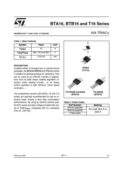
®1/9Table 1: Main FeaturesDESCRIPTIONAvailable either in through-hole or surface-mount packages, the BTA16, BTB16 and T16 triac series is suitable for general purpose AC switching. They can be used as an ON/OFF function in applica-tions such as static relays, heating regulation, in-duction motor starting circuits... or for phase control operation in light dimmers, motor speed controllers, ...The snubberless versions (BTA/BTB...W and T16series) are specially recommended for use on in-ductive loads, thanks to their high commutation performances. By using an internal ceramic pad,the BTA series provides voltage insulated tab (rat-ed at 2500V RMS ) complying with UL standards (File ref.: E81734).Symbol Value Unit I T(RMS)16A V DRM /V RRM 600, 700 and 800V I GT (Q 1)10 to 50mABTA16, BTB16 and T16 Series16A TRIAC SREV. 7February 2006SNUBBERLESS™, LOGIC LEVEL & STANDARDTable 2: Order CodesPart Number Marking BTA16-xxxxxRG See page table 8 onpage 8BTB16-xxxxxRG T16xx-xxxGBTA16, BTB16 and T16 Series2/9Table 3: Absolute Maximum Ratings Tables 4: Electrical Characteristics (T j = 25°C, unless otherwise specified)■SNUBBERLESS and Logic Level (3 quadrants)Symbol ParameterValue Unit I T(RMS)RMS on-state current (full sine wave)D 2PAK /TO-220AB T c = 100°C 16ATO-220AB Ins.T c = 15°C I TSM Non repetitive surge peak on-state current (full cycle, T j initial = 25°C) F = 50 Hz t = 20 ms 160A F = 60 Hz t = 16.7 ms168I ²t I ²t Value for fusingt p = 10 ms 144A ²s dI/dtCritical rate of rise of on-state cur-rent I G = 2 x I GT , t r ≤ 100 nsF = 120 HzT j = 125°C 50A/µs V DSM /V RSM Non repetitive surge peak off-state voltaget p = 10 msT j = 25°C V DSM /V RSM + 100V I GM Peak gate currentt p = 20 µsT j = 125°C 4A P G(AV)Average gate power dissipation T j = 125°C1W T stg T jStorage junction temperature range Operating junction temperature range- 40 to + 150- 40 to + 125°CSymbol Test ConditionsQuadrant T16BTA16 / BTB16Unit T1635SW CW BW I GT (1)V D = 12 V R L = 33 ΩI - II - III MAX.35103550mA V GT I - II - III MAX. 1.3V V GD V D = V DRM R L = 3.3 k ΩT j = 125°C I - II - IIIMIN.0.2V I H (2)I T = 500 mA MAX.35153550mA I L I G = 1.2 I GTI - III MAX.50255070mA II60306080dV/dt (2)V D = 67 %V DRM gate open T j = 125°C MIN.500405001000V/µs(dI/dt)c (2)(dV/dt)c = 0.1 V/µsT j = 125°C MIN.-8.5--A/ms(dV/dt)c = 10 V/µsT j = 125°C - 3.0--Without snubberT j = 125°C8.5-8.514BTA16, BTB16 and T16 Series3/9■Standard (4 quadrants)Table 5: Static Characteristics Table 6: Thermal resistance Symbol Test ConditionsQuadrant BTA16 / BTB16Unit C B I GT (1)V D = 12 V R L = 33 ΩI - II - III IV MAX.255050100mA V GT ALL MAX. 1.3V V GD V D = V DRM R L = 3.3 k Ω T j = 125°C ALLMIN.0.2V I H (2)I T = 500 mA MAX.2550mA I L I G = 1.2 I GTI - III - IVMAX.4060mA II 80120dV/dt (2)V D = 67 %V DRM gate openT j = 125°C MIN.200400V/µs (dV/dt)c (2)(dI/dt)c = 7 A/ms T j = 125°CMIN.510V/µsSymbol Test ConditionsValue Unit V T (2)I TM = 22.5 A t p = 380 µs T j = 25°C MAX. 1.55V V to (2)Threshold voltage T j = 125°C MAX.0.85V R d (2)Dynamic resistance T j = 125°C MAX.25m ΩI DRM I RRMV DRM = V RRMT j = 25°C MAX.5µA T j = 125°C2mANote 1: minimum I GT is guaranted at 5% of I GT max.Note 2: for both polarities of A2 referenced to A1.Symbol ParameterValue Unit R th(j-c)Junction to case (AC)D 2PAK / TO-220AB 1.2°C/WTO-220AB Insulated 2.1R th(j-a)Junction to ambient S = 1 cm ²D 2PAK45°C/WTO-220AB / TO-220AB Insulated60S = Copper surface under tab.BTA16, BTB16 and T16 Series4/9Figure 1: Maximum power dissipation versus RMS on-state current (full cycle)Figure 2: RMS on-state current versus case temperature (full cycle)Figure 3: RMS on-state current versus ambient temperature (printed circuit board FR4, copper thickness: 35µm) (full cycle)Figure 4: Relative variation of thermal impedance versus pulse durationFigure 5: On-state characteristics (maximum values)Figure 6: Surge peak on-state current versus number of cyclesBTA16, BTB16 and T16 Series5/9Figure 7: Non-repetitive surge peak on-state current for a sinusoidal pulse with width t p < 10 ms and corresponding value of I 2tFigure 8: Relative variation of gate trigger current, holding current and latching current versus junction temperature (typical values)Figure 9: Relative variation of critical rate of decrease of main current versus (dV/dt)c (typical values) (Snubberless & L ogic level types)Figure 10: Relative variation of critical rate of decrease of main current versus (dV/dt)c (typical values) (Standard types)Figure 11: D 2P AK Thermal resistance junction to ambient versus copper surface under tab (printed circuit board FR4, copper thickness: 35µm)BTA16, BTB16 and T16 Series6/9Figure 12: Ordering Information Scheme (BTA16 and BTB16 series)Figure 13: Ordering Information Scheme (T16 series)Table 7: Product SelectorPart Numbers Voltage (xxx)Sensitivity Type Package 600 V 700 V 800 V BTA/BTB16-xxxB X X X 50 mA Standard TO-220AB BTA/BTB16-xxxBW X X X 50 mA Snubberless TO-220AB BTA/BTB16-xxxCX X X 25 mA Standard TO-220AB BTA/BTB16-xxxCW X X X 35 mA Snubberless TO-220AB BTA/BTB16-xxxSW X XX 10 mA Logic level TO-220ABT1635-xxxGXX35 mASnubberlessD 2PAKBTB: non insulated TO-220AB packageBTA16, BTB16 and T16 Series Figure 14: D2PAK Package Mechanical DataFigure 15: D2PAK Foot Print Dimensions(in millimeters)7/9BTA16, BTB16 and T16 Series8/9In order to meet environmental requirements, ST offers these devices in ECOPACK® packages. These packages have a Lead-free second level interconnect . The category of second level interconnect is marked on the package and on the inner box label, in compliance with JEDEC Standard JESD97. The maximum ratings related to soldering conditions are also marked on the inner box label. ECOPACK is an ST trademark. ECOPACK specifications are available at: .Table 8: Ordering InformationOrdering type Marking Package Weight Base qtyDelivery modeBTA/BTB16-xxxyzRGBTA/BTB16xxxyz TO-220AB 2.3 g 50Tube T1635-xxxG T1635xxxG D 2PAK1.5 g50Tube T1635-xxxG-TRT1635xxxG1000Tape & reelNote: xxx = voltage, yy = sensitivity, z = typeTable 9: Revision HistoryDate Revision Description of ChangesOct-20026A Last update.13-Feb-20067TO-220AB delivery mode changed from bulk to tube.ECOPACK statement added.BTA16, BTB16 and T16 Series Information furnished is believed to be accurate and reliable. However, STMicroelectronics assumes no responsibility for the consequencesof use of such information nor for any infringement of patents or other rights of third parties which may result from its use. No license is granted by implication or otherwise under any patent or patent rights of STMicroelectronics. Specifications mentioned in this publication are subject to change without notice. This publication supersedes and replaces all information previously supplied. STMicroelectronics products are notauthorized for use as critical components in life support devices or systems without express written approval of STMicroelectronics.The ST logo is a registered trademark of STMicroelectronics.All other names are the property of their respective owners© 2006 STMicroelectronics - All rights reservedSTMicroelectronics group of companiesAustralia - Belgium - Brazil - Canada - China - Czech Republic - Finland - France - Germany - Hong Kong - India - Israel - Italy - Japan - Malaysia - Malta - Morocco - Singapore - Spain - Sweden - Switzerland - United Kingdom - United States of America9/9万联芯城-电子元器件采购网,提供一站式配套,解决物料烦恼,万联芯城是国内优质的电子元器件供应商,货源渠道来自原厂及代理商,只售原装现货,只需提交BOM物料清单,我们将为您报出一个满意的价格,解决客户采购烦恼,为客户节省采购成本,点击进入万联芯城。
双向可控硅为什么称为“TRIAC”?三端:TRIode(取前三个字母)交流半导体开关:AC-semiconductor switch(取前两个字母)以上两组名词组合成“TRIAC”,或“TRIACs”中文译意“三端双向可控硅开关”。
由此可见“TRIAC”是双向可控硅的统称。
另:双向:Bi-directional(取第一个字母)控制:Controlled (取第一个字母)整流器:Rectifier (取第一个字母)再由这三组英文名词的首个字母组合而成:“BCR”,中文译意:双向可控硅。
以“BCR”来命名双向可控硅的典型厂家如日本三菱,如:BCR1AM-12、BCR8KM、BCR08AM 等等。
--------------双向:Bi-directional (取第一个字母)三端:Triode (取第一个字母)由以上两组单词组合成“BT”,也是对双向可控硅产品的型号命名,典型的生产商如:意法ST公司、荷兰飞利浦-Philips公司,均以此来命名双向可控硅.代表型号如:PHILIPS 的BT131-600D、BT134-600E、BT136-600E、BT138-600E、BT139-600E、、等。
这些都是四象限/非绝缘型/双向可控硅;Philips公司的产品型号前缀为“BTA”字头的,通常是指三象限的双向可控硅。
三象限的品种主要应用于电机电路、三相市电输入的电路、承受的瞬间浪涌电流高。
-------------------而意法ST公司,则以“BT”字母为前缀来命名元件的型号,并且在“BT”后加“A”或“B”来表示绝缘与非绝缘。
组成:“BTA”、“BTB”系列的双向可控硅型号,如:四象限、绝缘型、双向可控硅:BTA06-600C、BTA08-600C、BTA10-600B、BTA12-600B、BTA16-600B、BTA41-600、、、等等;四象限、非绝缘、双向可控硅:BTB06-600C、BTB08-600C、BTB10-600B、BTB12-600B、BTB16-600B、BTB41-600、、、等等;ST公司所有产品型号的后缀字母(型号最后一个字母)带“W”的,均为“三象限双向可控硅”。

1/7®BTA/BTB16 and T16 SeriesSNUBBERLESS ™ , LOGIC LEVEL & STANDARD16A TRIAC SApril 2002 - Ed: 5AMAIN FEATURES:DESCRIPTIONAvailable either in through-hole or surface-mount packages, the BTA/BTB16 and T16 triac series is suitable for general purpose AC switching. They can be used as an ON/OFF function in applications such as static relays, heating regulation, induction motor starting circuits... or for phase control operation in light dimmers, motor speed controllers, ...The snubberless versions (BTA/BTB...W and T16series) are specially recommended for use on inductive loads, thanks to their high commutation performances. By using an internal ceramic pad,the BTA series provides voltage insulated tab (rated at 2500V RMS) complying with UL standards (File ref.: E81734).Symbol Value Unit I T(RMS)16A V DRM /V RRM 600 and 800VI GT (Q 1)10 to 50mAABSOLUTE MAXIMUM RATINGSSymbol ParameterValueUnit I T(RMS)RMS on-state current (full sine wave)D2²P AK Tc = 100°C 16ATO-220ABTO-220AB Ins.Tc = 85°C I TSM Non repetitive surge peak on-state current (full cycle, Tj initial = 25°C) F = 60 Hz t = 16.7 ms 168A F = 50 Hzt = 20 ms160I ²t I ²t Value for fusingtp = 10 ms144A ²s dI/dtCritical rate of rise of on-state current I G = 2 x I GT , tr ≤ 100 nsF = 120 Hz Tj = 125°C 50A/µs V DSM /V RSM Non repetitive surge peak off-statevoltagetp = 10 ms Tj = 25°C V DRM /V RRM+ 100V I GM Peak gate currenttp = 20 µsTj = 125°C 4A P G(AV)Average gate power dissipation Tj = 125°C1W T stg T jStorage junction temperature range Operating junction temperature range- 40 to + 150- 40 to + 125°CBTA/BTB16 and T16 Series2/7ELECTRICAL CHARACTERISTICS (Tj = 25°C, unless otherwise specified)sSNUBBERLESS™ and LOGIC LEVEL (3 Quadrants)sSTANDARD (4 Quadrants)STATIC CHARACTERISTICSNote 1: minimum IGT is guaranted at 5% of IGT max.Note 2: for both polarities of A2 referenced to A1Symbol Test ConditionsQuadrantT16BTA/BTB16UnitT1635SW CW BW I GT (1)V D = 12 V R L = 33 ΩI - II - III MAX.35103550mA V GT I - II - III MAX. 1.3V V GD V D = V DRM R L = 3.3 k Ω Tj = 125°C I - II - IIIMIN.0.2V I H (2)I T = 500 mA MAX.35153550mA I L I G = 1.2 I GTI - III MAX.50255070mA II60306080dV/dt (2)V D = 67 % V DRM gate open Tj = 125°C MIN.500405001000V/µs (dI/dt)c (2)(dV/dt)c = 0.1 V/µs Tj = 125°CMIN.-8.5--A/ms(dV/dt)c = 10 V/µs Tj = 125°C - 3.0--Without snubber Tj = 125°C8.5-8.514Symbol Test ConditionsQuadrant BTA/BTB16UnitCB I GT (1)V D = 12 V R L = 33 ΩI - II - III IV MAX.255050100mA V GT ALL MAX. 1.3V V GD V D = V DRM R L = 3.3 k Ω Tj = 125°C ALLMIN.0.2V I H (2)I T = 500 mA MAX.2550mA I L I G = 1.2 I GTI - III - IVMAX.4060mA II80120dV/dt (2)V D = 67 % V DRM gate open Tj = 125°CMIN.200400V/µs (dV/dt)c(2)(dI/dt)c = 7 A/ms Tj = 125°CMIN.510V/µsSymbol Test ConditionsValue Unit V TM (2)I TM = 22.5 A tp = 380 µs Tj = 25°C MAX. 1.55V V to (2)Threshold voltage Tj = 125°C MAX.0.85V R d (2)Dynamic resistance Tj = 125°C MAX.25m ΩI DRM I RRMV DRM = V RRMTj = 25°C MAX.5µA Tj = 125°C2mABTA/BTB16 and T16 Series3/7THERMAL RESISTANCESS: Copper surface under tabPRODUCT SELECTORORDERING INFORMATIONSymbol ParameterValue Unit R th(j-c)Junction to case (AC)D ²PAK TO-220AB 1.2°C/WTO-220AB Insulated2.1R th(j-a)Junction to ambientS = 1 cm ²D ²PAK 45°C/WTO-220AB 60TO-220AB InsulatedPart NumberVoltage(xxx)SensitivityTypePackage600 V800 V BTA/BTB16-xxxB X X 50 mA Standard TO-220AB BTA/BTB16-xxxBW X X 50 mA Snubberless TO-220AB BTA/BTB16-xxxC X X 25 mA Standard TO-220AB BTA/BTB16-xxxCW X X 35 mA Snubberless TO-220AB BTA/BTB16-xxxSW X X 10 mA Logic level TO-220AB T1635-xxxGXX35 mASnubberlessD ²PAKBTA/BTB16 and T16 Series4/7OTHER INFORMATIONNote: xxx = voltage, y = sensitivity, z = typePart NumberMarkingWeight Base quantity Packing mode BTA/BTB16-xxxyz BTA/BTB16xxxyz 2.3 g 250Bulk BTA/BTB16-xxxyzRG BTA/BTB16-xxxyz 2.3 g 50Tube T1635-xxxG T1635xxxG 1.5 g 50Tube T1635-xxxG-TRT1635xxxG1.5 g1000T ape & reelFig. 1: Maximum power dissipation versus RMS on-state current (full cycle).Fig. 2-1: RMS on-state current versus case temperature (full cycle).Fig. 2-2: D²PAK RMS on-state current versus ambient temperature (printed circuit board FR4,copper thickness: 35µm), full cycle.Fig. 3: Relative variation of thermal impedance versus pulse duration.BTA/BTB16 and T16 Series5/7Fig. 4: On-state characteristics (maximum values)Fig. 5: Surge peak on-state current versus number of cycles.Fig. 6: Non-repetitive surge peak on-state current for a sinusoidal pulse with width tp <10ms, and corresponding value of I²t.Fig. 7: Relative variation of gate trigger current,holding current and latching current versus junction temperature (typical values).Fig. 8: Relative variation of critical rate of decrease of main current versus (dV/dt)c (typical values).Fig. 9: Relative variation of critical rate of decrease of main current versus junction temperature.BTA/BTB16 and T16 SeriesFig. 10:D²P AK Thermal resistance junction to ambient versus copper surface under tab (printed circuit board FR4, copper thickness: 35µm).PACKAGE MECHANICAL DATA6/7BTA/BTB16 and T16 Series PACKAGE MECHANICAL DATAFOOTPRINT DIMENSIONS (in millimeters)Information furnished is believed to be accurate and reliable. However, STMicroelectronics assumes no responsibility for the consequences of use of such information nor for any infringement of patents or other rights of third parties which may result from its use. No license is granted by implication or otherwise under any patent or patent rights of STMicroelectronics. Specifications mentioned in this publication are subject to change without notice. This publication supersedes and replaces all information previously supplied. STMicroelectronics products are not authorized for use as critical components in life support devices or systems without express written approval of STMicroelectronics.© The ST logo is a registered trademark of STMicroelectronics© 2002 STMicroelectronics - Printed in Italy - All Rights ReservedSTMicroelectronics GROUP OF COMPANIESAustralia - Brazil - Canada - China - Finland - France - GermanyHong Kong - India - Isreal - Italy - Japan - Malaysia - Malta - Morocco - SingaporeSpain - Sweden - Switzerland - United Kingdom - United States.7/7。