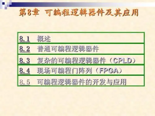
数字逻辑电路(英文版)课后习题答案第8章
- 格式:doc
- 大小:348.50 KB
- 文档页数:5

第8章习题及解答8.1 在图8.3(a )用5G555定时器接成的施密特触发电路中,试问:(1)当CC 12V V =时,而且没有外接控制电压时,T+V 、T-V 和T V ∆各为多少伏?(2)当CC 10V V =时,控制电压CO 6V V =时,T+V 、T-V 和T V ∆各为多少伏?题8.1 解:⑴ 283T CC V V V +== , 143T CC V V V -==, V V V V T T T 4=-=∆-+;⑵ 6T CO V V V +== , 132T CO V V V -== ,3T T T V V V V +-∆=-=。
8.3 图P8.3(a )为由5G555构成的单稳态触发电路,若已知输入信号i V 的波形如图P8.3(b )所示,电路在t=0时刻处于稳态。
(1)根据输入信号i V 的波形图定性画出C V 和输出电压O V 对应的波形。
(2)如在5G555定时器的5脚和1脚间并接一只10K 的电阻,试说明输出波形会发生怎样的变化?OiV(a ) (b )图 P8.3题8.3 解:(1)对应的波形如图题解8.3(a )所示。
i VV V图 题解8.3(a )(2)如在5G555定时器的5脚和1脚间并接一只10K 的电阻,则输出脉冲宽度W1t 等于电容电压C V 从0上升到CC 1115V=7.5V 22V =⨯所需时间,因此输出脉冲宽度W1t 要比图题解8.3(a )波形中W t 窄。
对应的波形如图题解8.3(b )所示。
i VV V 图 题解8.3(b )8.5 图P8.5(a )所示是用集成单稳态触发电路74121和D 触发器构成的噪声消除电路,图P8.5(b )为输入信号。
设单稳态触发电路的输出脉冲宽度W t 满足n W s t t t <<(其中n t 为噪声,s t 为信号脉宽),试定性画出Q 和O V 的对应波形。
图 P8.5题8.5 解:波形图如图题解8.5所示。
84题8.1.1集成555电路在CO 端不使用时,比较器C l 的基准电压为 , C 2的基准电压为 。
(A )2U DD /3 (B )U DD /3 (C )U DD (D )U DD /2 答:A 、B题8.1.2 集成7555电路在控制电压端CO 处加控制电压U CO ,则C 1和C 2的基准电压将分别变为 。
(A )2U CO /3 (B )U CO /3 (C )U CO (D )U CO /2 答:C 、D题8.1.3 为使集成555电路输出OUT 为低电平,应满足 条件。
(A )R 为低电平 (B )TR <U DD /3 (C )TH <2U DD /3 (D )TH >2U DD /3 答:A 、D题8.1.4 集成555电路在输出OUT 前端设置了缓冲器G 2的主要原因是 。
(A )提高高电平 (B )减低低电平(C )提高驱动负载能力 (D )放电端(D )电平和输出端(OUT )保持一致 答:C 、D题8.2.1施密特触发器属于 型电路。
(A )电平触发 (B )边沿触发 (C )脉冲触发 (D )锁存器 答:A题8.2.2 施密特触发器的+th U 称为正向阈值电压,-th U 称为负向阈值电压,且+th U >-th U ,二者的差值称回差为 。
(A )+th U +-th U (B )+th U --th U (C )+th U (D )-th U答:B题8.2.3 用运算放大器组成的施密特触发器利用了 特性。
(A )正反馈 (B )线性(C )负反馈 (D )输出正饱和值与负饱和值 答:A 、D题8.2.4 施密特触发器主要作用是 、 、 等。
(A )信号整形 (B )波形变换 (C )提高驱动负载能力 (D )幅度鉴别 答:A 、B 、D题8.2.5施密特触发器用于整形时,输入信号的幅度应 。
(A )大于+th U (B )等于+th U (C )等于-th U(D )小于-th U题8.2.6 可将变化缓慢的输入信号变换为矩形脉冲信号。
思考题与习题8-1 试问一个256字×4位的ROM应有地址线、数据线、字线和位线各多少根?8根地址线,4根数据线,字线即行选线,8根;位线即列选线,4根。
8-2 用一个2线-4线译码器和4片1024×8位的ROM组成一个容量为4096×8位的ROM,请画出连线图。
电路为字扩展方式。
2线-4线译码器的输出为低电平有效,分别接至四片1024×8位的ROM 的,将地址线、输出线对应连接。
图略。
8-3 确定用ROM实现下列逻辑函数所需的容量:(1)比较两个四位二进制数的大小及是否相等;(2)两个三位二进制数相乘的乘法器;(3)将8位二进制数转化为十进制数的转化电路。
(1) 根据题意,两个四位数比较的结果有相等,大于或者小于三种结果,因此输入为8位,输出为三位,ROM容量为:28×3=768(2)最大的三位二进制数为7×7=49=110001B,因此输出为6位;则ROM的容量为26×6=384(3)最大的八位二进制数为255,因此输出为3位,而输入为8位,则其ROM容量为28×3=7688-4 图8-4为256×4位RAM芯片的逻辑电路图,请用位扩展的方法组成256×8位的RAM,画出逻辑连线图。
将两片的地址输入信号分别相连,用同一个信号控制8个相同字数的RAM,输出分别为两片的4位输出,就可达到扩展输出的结果,图略。
8-5 试用EFPOM实现74LS49的功能。
74LS49为7段显示译码器,输入为4位,输出为7为,根据74LS49的功能表,可写出输出a,b,c,d,e,f,g的表达式。
用或阵列,经过输出缓冲器,得到输出a,b,c,d,e,f,g。
图略。
1。
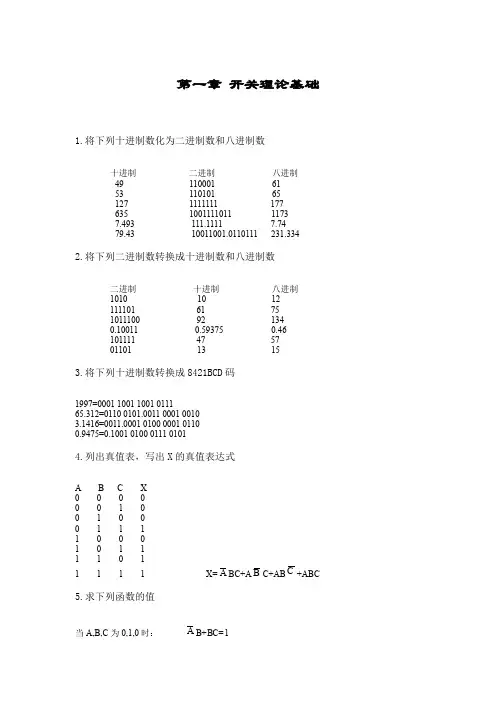
Digital Logic Circuits 数字逻辑电路智慧树知到课后章节答案2023年下南京理工大学南京理工大学第一章测试1.The number of values that can be assigned to a bit are ( )答案:twopared to analog systems, digital systems ( )答案:are less prone to noise3.The term bit means ( )答案:both answers (b) and (c)4. A quantity has continuous value is ( )答案:an analog quantity5.Verilog HDL is a ( )答案:computer language6. A category of digital integrated circuits having functions that can be altered isknown as fixed-function logic.答案:错7.Data are information only in numeric.答案:错8.Two broad types of digital integrated circuits are fixed-function andprogrammble.答案:对9.The nonrecurring engineering (NRE) cost for an ASIC design is normally low.答案:错10.There is an “invalid” region between the input ranges for logic 0 and logic 1答案:对第二章测试1.For the binary number 10000, the weight of the column with the 1 is ( )答案:162.The 2’s complement of 1000 is ( )答案:10003.The fractional binary number 0.11 has a decimal value of ( )答案:¾4.The number 1100 in BCD is ( )答案:invalid5.An example of an unweighted code is ( )答案:Gray code6.An example of an alphanumeric code is ( )答案:ASCII7.The overflow occurs when adding the following 8-bit two’s complementnumber:01011101+00110001答案:对8.The overflow does NOT occur when adding the following 8-bit two’scomplement number:10111111+11011111答案:对9.In general, we need at most bits to express the product when multiplying ann-bit number by an m-bit number.答案:错10.An addition overflows if the addends’ signs are the same but the sum’s sign isdifferent from the addends’.答案:对第三章测试1.The Boolean expression A. 1 is equal to ( ).答案:A2.The Boolean expression A + 1 is equal to ( ).答案:13.The Boolean equation AB + AC = A(B+ C) illustrates ( )答案:the distribution law4.The associative law for addition is normally written as ( )答案:(A + B) + C = A + (B + C)5. A Boolean expression that is in standard SOP form is ( )答案:has every variable in the domain in every term6.Adjacent cells on a Karnaugh map differ from each other by答案:one variable7.SOP standard form is useful for constructing truth tables or for implementinglogic in PLDs.答案:对8.Logic simplification is still useful in nowadays FPGA designs.答案:错9.In synthesis, a netlist will be generated to describe the circuit completely.答案:对10.In FPGA design, the step that “maps” the design from the netlist to fit it to atarget device is known as "programming".答案:错第四章测试1.The 74138 decoder can also be used as ( ).答案:a DEMUX2.Assume you want to decode the binary number 0011 with an active-LOWdecoder. The missing gate should be ( ).答案:a NAND gate3.To expand a 2-bit parallel adder to a 4-bit parallel adder, you must ( ).答案:use two 2-bit adders with the carry output of one connected to the carry input of the other4.If an hex-to-binary priority encoder has its 0, 3, 6, and 14 inputs at the activelevel, the active-HIGH binary output is ( ).答案:11105.The continuous assignmentassign OUT = select ? A : B;specifies the condition that OUT = ( )if select = 1, else OUT = ( )if select = 0.答案:A, B6.Consider the initial block in the following:initialbeginA = 0;B = 0;#10 A = 1;#20 A = 0; B = 1;EndThen at t = 30, A is changed to ( ) and B to ( ).答案:0,17.The initial statement executes only once, starting from simulation time 0,and may continue with any operations that are delayed by a given number of time units.答案:对8.In Verilog HDL, the definitions of modules are allowed to be nested.答案:错9.The value z represents an unknown logic value in Verilog HDL.答案:错10.In Verilog HDL, ~(1010) is (0101), and !(1010) is 0.答案:对第五章测试1. The output of a D latch will not change if ( ).答案:Enable is not active2.The D flip-flop shown will ( ).答案:toggle on the next clock pulse3.For the J-K flip-flop shown, the number of inputs that are asynchronous is( ).答案:24.Assume the output is initially HIGH on a leading edge triggered J-K flip flop.For the inputs shown, the output will go from HIGH to LOW on which clock pulse?答案:35.The time interval illustrated is called ( ).答案:t PLH6.The advantage of dynamic RAM over static RAM is that ( ).答案:it is simpler and cheaper7.An asynchronous reset signal will override the clock on a FF.答案:对8.In Verilog HDL, an initial behavioral statement executes only once.答案:对9.In a Moore model, the outputs of the sequential circuit are not synchronizedwith the clock.答案:错10.The output of the Mealy machine is the value that is present immediatelybefore the active edge of the clock.答案:对第六章测试1.To cause a D flip-flop to toggle, connect the ( ).答案:2. A 4-bit binary counter has a terminal count of ( ).答案:153.Assume the clock for a 4-bit binary counter is 80 kHz. The output frequencyof the fourth stage (Q3) is ( ).答案:5 kHz4. A 4-bit parallel-in/parallel-out shift register will store data for ( ).答案:1 clock period5.An advantage of a ring counter over a Johnson counter is that the ringcounter ( ).答案:is self-decoding6. A possible sequence for a 4-bit ring counter is ( ).答案:… 1000, 0100, 0010 …7. A divide‐by‐N-counter is a counter that goes through a repeated sequence ofN states, and it is also known as a modulo‐N counter.答案:对8.For counters with unused states, it is necessary to ensure that the circuiteventually goes into one of the valid states so that it can resume normaloperation.答案:对9.For transmission, data from a UART is sent in synchronous parallel form.答案:错10.The maximum modulus of a counter is , where n is the number of stages (flip-flops) in the counter.答案:错第七章测试1.Static RAM is ( ).答案:volatile read/write memory2. A nonvolatile memory is one that ( )答案:retains data without power applied3.The advantage of dynamic RAM over static RAM is that ( ).答案:it is simpler and cheaper4. A 4-bit parallel-in/parallel-out shift register will store data for ( ).答案:1 clock period5.When data is read from RAM, the memory location is ( ).答案:unchanged6.The first step in a read or write operation for a random access memory is to( ).答案:place a valid address on the address bus7.Address multiplexing can reduce the number of pins in the IC package.答案:对8.One of the major applications of SRAMs is in cache memories in computers.答案:对9.RAM is used in a computer to store the BIOS (Basic Input/Output System.答案:错10.Memory expansion is accomplished by adding an appropriate number ofmemory chips to the address, data, and control buses.答案:对第八章测试1.The number of comparators required in a 10-bit flash ADC is ( ).答案:10232.If an anti-aliasing filter is not used in digitizing a signal the recovery process( )答案:may include alias signals3.An anti-aliasing filter should have ( )答案:4. A reconstruction filter ( ).答案:all of the above5.The ( ) of the A/D converter determines how close the actual digital outputis to the theoretically expected digital output for a given analog input.答案:accuracy6.The ( ) of ADC is determined by the number of bits it uses to digitize an inputsignal.答案:resolution7.An ADC is an analog data component答案:错8. A higher sampling rate is more accurate than a lower sampling rate for agiven analog signal.答案:对9.Two types of DAC are the binary-weighted input and the R/2R ladder.答案:对10.The Integral Nonlinearity of an ADC defines the maximum deviation of theADC transfer function from the best-fit line.答案:对。
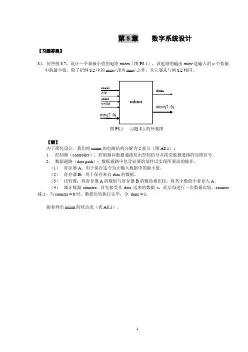
第8章 数字系统设计【习题答案】8.1 仿照例8.2,设计一个求最小值的电路minm (图P8.1),该电路的输出minv 是输入的n 个数据中的最小值。
除了把例8.2中的maxv 改为minv 之外,其它要求与例8.2相同。
minmreset clk start validdata(7..0)doneminv(7..0)图P8.1 习题8.1的外观图【解】为了简化设计,我们将minm 的电路结构分解为2部分(图A8.1):1. 控制器(controller ):控制器向数据通路发出控制信号并接受数据通路的反馈信号。
2. 数据通路(data path ):数据通路中包含必要的部件以实现所要求的操作。
(1) 寄存器A :用于保存迄今为止输入数据中的最小值。
(2) 寄存器B :用于保存来自data 的数据。
(3) 比较器:将寄存器A 的数值与寄存器B 的数值相比较,将其中数值小者存入A 。
(4) 减计数器counter :首先接受从data 送来的数据n ,此后每进行一次数据比较,counter 减1,当counter = 0时,数据比较执行完毕,令 done = 1。
接着列出minm 的状态表(表A8.1)。
图A8.1 minm的电路分解以下为VHDL行为描述:LIBRARY ieee;USE ieee.std_logic_1164.ALL;USE ieee.std_logic_unsigned.ALL;ENTITY minm ISPORT(reset, clk, start, valid : IN std_logic;data : IN std_logic_vector( 7 DOWNTO 0 );minv : OUT std_logic_vector(7 DOWNTO 0 );done : OUT std_logic );END minm;ARCHITECTURE behav OF minm ISCONSTANT st0 : std_logic_vector( 2 DOWNTO 0 ) := "000" ; CONSTANT st1 : std_logic_vector( 2 DOWNTO 0 ) := "001" ; CONSTANT st2 : std_logic_vector( 2 DOWNTO 0 ) := "011" ; CONSTANT st3 : std_logic_vector( 2 DOWNTO 0 ) := "111" ; CONSTANT st4 : std_logic_vector( 2 DOWNTO 0 ) := "101" ; CONSTANT st5 : std_logic_vector( 2 DOWNTO 0 ) := "100" ; CONSTANT st6 : std_logic_vector( 2 DOWNTO 0 ) := "110" ; SIGNAL A, B, counter : std_logic_vector(7 DOWNTO 0 ); SIGNAL state : std_logic_vector( 2 DOWNTO 0 );BEGINcompare_process:PROCESS(reset, clk, state )BEGINIF (reset = '1') AND rising_edge( clk ) THENCASE state ISWHEN st0 =>A <= "11111111";B <= "11111111";minv <= "00000000";done <= '0';WHEN st1 =>IF valid = '1' THENcounter <= data;END IF;WHEN st2 =>NULL;WHEN st3 =>IF valid = '1' THENIF A > B THENA <= B;END IF;B <= data;counter <= counter - 1;END IF;WHEN st4 =>NULL;WHEN st5 =>NULL;WHEN OTHERS =>IF A > B THENminv <= B;ELSEminv <= A;END IF;done <= '1';END CASE;END IF;END PROCESS;state_process:PROCESS( reset, clk )BEGINIF reset = '0' THENstate <= st0;ELSIF rising_edge( clk ) THENCASE state ISWHEN st0 =>IF start = '1' THENstate <= st1;END IF;WHEN st1 =>IF valid = '1' THENstate <= st2;END IF;WHEN st2 =>IF valid = '0' THENstate <= st3;END IF;WHEN st3 =>IF valid = '1' THENstate <= st4;END IF;WHEN st4 =>IF valid = '0' THENstate <= st5;END IF;WHEN st5 =>IF counter = "00000000" THENstate <= st6;ELSEstate <= st3;END IF;WHEN OTHERS =>IF start = '1' THENstate <= st0;END IF;END CASE;END IF;END PROCESS;END behav;将上述VHDL代码作为QuartusⅡ的输入,经过编译、模拟等操作后,得到求最小值电路minm 的功能模拟波形,分析如下:1.首先令reset = 0,使电路进入初始状态st0。

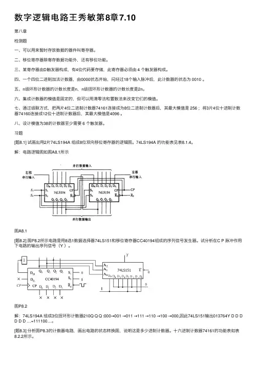
数字逻辑电路王秀敏第8章7.10第⼋章检测题⼀、可以⽤来暂时存放数据的器件叫寄存器。
⼆、移位寄存器除寄存数据功能外,还有移位功能。
三、某寄存器由D触发器构成,有4位代码要存储,此寄存器必须由 4 个触发器构成。
四、⼀个四位⼆进制加法计数器,由0000状态开始,问经过18个输⼊脉冲后,此计数器的状态为 0010 。
五、n级环形计数器的计数长度是n,n级扭环形计数器的计数长度是2n。
六、集成计数器的模值是固定的,但可以⽤清零法和置数法来改变它们的模值。
七、通过级联⽅式,把两⽚4位⼆进制计数器74161连接成为8位⼆进制计数器后,其最⼤模值是 256 ;将3⽚4位⼗进制计数器74160连接成12位⼗进制计数器后,其最⼤模值是4096 。
⼋、设计模值为38的计数器⾄少需要 6 个触发器。
习题[题8.1] 试画出⽤2⽚74LS194A 组成8位双向移位寄存器的逻辑图。
74LS194A 的功能表见表8.1.4。
解:电路逻辑图如图A8.1所⽰图A8.1[题8.2] 图P8.2所⽰电路是⽤8选1数据选择器74LS151和移位寄存器CC40194组成的序列信号发⽣器。
试分析在C P 脉冲作⽤下电路的输出序列信号(Y )。
图P8.2解:74LS194A 组成3位扭环形计数器210Q Q Q :000→001 →011 →111 →110 →100 →000,因此74LS151输出013764Y D D D D D D …=111100…。
[题8.3] 分析图P8.3的计数器电路,画出电路的状态转换图,说明这是多少进制计数器。
⼗六进制计数器74161的功能表如表8.2.2所⽰。
图P8.3解:采⽤同步预置数法,31LD Q Q =。
计数器起始状态为0011,结束状态为1010,所以该计数器为⼋进制加法计数器。
状态转换图略。
[题8.4] 分析图P8.4的计数器电路,说明这是多少进制的计数器,并画出电路的状态转换图。
⼗进制计数器74160的功能表如表8.2.6所⽰。
第七章 存储器和可编程器件7—1 填空1.半导体存储器按功能分有_RAM __和__ROM _两种。
2.ROM 主要由__存储矩阵____和__地址译码器____和输出缓冲器三部分组成,按照工作方式的不同进行分类,ROM 可分为_MROM __、_PROM __和_EPROM __三种。
3.某EPROM 有位8数据线,13位地址线,则其存储容量为_8K ×8b __。
4.随机存储器按照存储原理可以分为_____SRAM ______和___DRAM ________,其中______DRAM_____由于具有“漏电”特性,因此需要进行_____刷新______操作。
7—2 图7.2是16⨯4位ROM ,3A 2A 1A 0A 为地址输入,3D 2D 1D 0D 为数据输出,试分别写出3D 2D 1D 0D 的逻辑表达∑=)15,10,6,2(3m D ∑=)15,12,11,8,7,4,3(2m D ∑=)12,9,6,3,0(1m D ∑=)14,13,12,11,8,7,6,5,2,0(0m D7—3 由一个三位二进制加法计数器和一个ROM 构成的电路如图7.3(a )所式。
1. 写出输出1F 2F 3F 的表达式;2. 画出CP 作用下1F 2F 3F 的波形(计数器的初态为“0”)。
答:∑=)5,4,2,1(1m F ∑=)6,5,3(2m F∑=)6,5,4,2,1,0(3m F2、波形如图所示。
注意:F 为组合逻辑。
A A A A 3210图7.2123F F F 图7.3(a )123F F F 图7.3(a )图7.3(b )W 7第8章 脉冲波形的产生及整形8-1 图8.1(a )为由555定时器和D 触发器构成的电路,请问: 1. 555定时器构成的是哪种脉冲电路? 2. 在图(b )中画出C U O1U O2U 的波形; 3. 计算O1U O2U 的频率;4. 如果在555定时器的第5脚接入4V 的电压源,则O1U 的频率将为多少?答:1、该电路为多谐振荡器。
初中英语八大时态综合时态练习( )1. What _____ you _____ over the weekend?A. will; doB. does; doC. did; doD. were,; doing ( )2. Xiao Li usually _____ to school by bike last year.A. goesB. wentC. will goD. is going( )3. What _____ in our town 100 years from now?A. happenedB. is happenedC. has happenedD. will happen ( )4. Mr. Smith _____ to see you in an hour.A. cameB. has comeC. will comeD. comes( )5. _____ you _____ from your parents recently?A. Did; hearB. Have; heardC. Do; hearD. Will; hear ( )6. We _____ TV at home this time last night.A. were watchingB. watchedC. have watchedD. would watch ( )7. We _____ over 1500 English words by the end of last month.A. have learnedB. had learnedC. will learnD. learnt( )8. She _____ in Shanghai for ten years since 1992.A. has livedB. had livedC. livedD. will live( )9. She _____ in Shanghai for ten years.A. has livedB. had livedC. livedD. will live( )10. We all know that the earth _____ round the sun.A. goesB. wentC. is goingD. will go( )11. “Where are the boys?”“They _____ soccer on the playground.”A. playB. are playingC. were playingD. played( )12. Look! Lucy _____ under the tree.A. readsB. is readingC. was readingD. read( )13. He _____ more than 200 model cars in the last five years.A. has collectedB. had collectedC. collectedD. will collect( )14. Jim _____ a letter to his parents at 7:30 last night.A. had writtenB. wroteC. would writeD. was writing ( )15. The Smiths _____ in Beijing since two weeks ago.A. stayedB. were stayingC. would stayD. have stayed ( )16. “When _____ you _____ the bike?”“Last Monday.”A. have; boughtB. did; buyC. will; buyD. do; buy( )17. Look! The boy _____English now.A. likesB. likedC. is likingD. was liking( )18. Most students in our class _____ TV twice a week.A. watchB. watchedC. will watchD. are watching ( )19. How soon _____ they _____ back from work?A. do; comeB. did; comeC. have; comeD. will; come( )20. “Where _____ you _____ Mr. Li?”“In his office, half an hour ago.”A. will; seeB. did; seeC. have, seenD. do; see( )21. I _____ a new dictionary. Look! It’s very useful.A. boughtB. will buyC. have boughtD. would buy。
习题8.1 解释下列名词:分辨率、转换精度、转换时间、量化、量化单位。
略(见书)8.2 数字量和模拟量有何区别?D/A 转换和A/D 转换在数字系统中有何主要作用? 略(见书)8.3 一个D/A 转换器应包含哪几部分,它们的功能是什么? 略(见书)8.4 一个8位D/A 转换器的分辨率为多少? 解:n 位D/A 转换器的分辨率为121n-,因此8位D/A 转换器的分辨率为814%21=-。
8.5 图8.4所示电路为4位T 形电阻D/A 转换器。
1)试分析其工作原理,求出V O 的表达式; 2)如果已知n=8位的D/A 转换器中,V REF =-10V ,R f =3R ,输入D=11010100时,输出电压值;3)如果R f =2R ,对应(2)中的输出电压V O 又是多少?解:1)S 3、S 2、S 1、S 0为模拟开关,分别受输入代码d 3、d 2、d 1、d 0的状态控制,也就是说输入代码的高低电平状态可控制流入集成运放A 反相输入端的电流,也就控制了输出电压的大小。
从而使得输出电压与输入的数字代码成比例关系。
输出电压表达式为:3210R E F O 32104321R E F R E F 321044(2222)323(2222)22V V d d d d R R V V d d d d D=-⨯+⨯+⨯+⨯⋅⋅=-⨯+⨯+⨯+⨯=-2)如果已知n =8位的D/A 转换器中,V REF =-10V ,R f =3R ,输入D =11010100时,同理可推出n =8位的D/A 转换器的输出电压R E F O 82V V D =-,即O 8.3V V ≈。
3)如果R f =2R ,对应(2)中的输出电压为R E F R E F O 88222332V V V D R D R=-⋅=-⋅⋅。
8.6 一个8位D/A 转换器,求:1)最小输出电压增量V LSB =0.02V ,当输入代码为01001101时,输出电压V O 为多少?2)若其分辨率用百分数表示,则为多少?3)若某一系统中要求的精度为0.25%,能不能用该D/A 转换器。
CH8部分答案
8.13 what is the counting sequence of the circuit shown in Figure X8.13
74×169的工作特性:
顺序计数到1111以及逆序计数到0000时,RCO_L 有效。
所以,可画出状态转移图
8.14 A 74×163 counter is hooked up with inputs ENP, ENT, and D always HIGH, inputs A , B and C always LOW, input LD_L=(QA ·QC)’, and input CLR_L=(QB ·QD)’, The CLK input is hooked up to a free-running clock signal. Draw a logic diagram for this circuit. Assuming that the counter starts in state 0000, write the output sequence on QD QC QB QA for the next 15 clock ticks. 解:
QD QC QB QA=0101时,计数器置数,装入DCBA=1000;
QD QC QB QA=1010时,计数器清零;
状态:QD QC QB QA=0000,0001,0010,0011,0100,0101,1000,1001,1010,0000,0001,0010,0011,0100,0101
8.16
According to figure 8-51 and table 8-26, the 5-bit LFSR’s feedback equation is X5=X2⊕X0,
so we can draw the circuit as following:
And the X5=1111100011011101010000100101100(31 bit)
The simulation graphic:
As starting state 0001, if X4=0,then the first ten state 00001→10000→01000→00100→10010→01001→10100→11010→01101→00110→10011→11001→11100….
8.26 将Q接T输入(教材T触发器)(或接入时钟端,教学ppt图)
8.27
8.35Using a 74×163 4-bit binary counter,design a modulo-11counter circuit with the counting sequence4,5,……13,14,4,5,6……
8.38 Design a modulo-129 counter using only two 74×163s and no additional gates.
解:
因为不能使用除163外的其他门,所以只能从计数值本身的特点来考虑。
.
0~127,最高位是0,128~255,最高位是1。
LD_L,CLR_l均为低电平有效,显然只能利用模129中唯一一次出现0的位来进行置数或清零。
清零方式不可行。
考虑置数方式:
考虑最高位,若用128~255和0,一共有129个数,且除0以外,其余数的最高位都是1,
所以,从255计数到0时,利用最高位去置数。
8.55
8.57 2-bit升序计数器
2-bit降序计数器
8.58。