飞思卡尔芯片简介
- 格式:pdf
- 大小:710.11 KB
- 文档页数:12
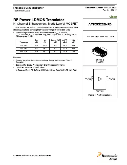
RF Power LDMOS TransistorN--Channel Enhancement--Mode Lateral MOSFETThis 80watt RF power LDMOS transistor is designed for cellular base station applications covering the frequency range of 720to 960MHz.•Typical Single--Carrier W--CDMA Performance:V DD =28Volts,I DQ =1400mA,P out =80Watts Avg.,Input Signal PAR =7.5dB @0.01%Probability on CCDF.Frequency G ps (dB)ηD (%)Output PAR(dB)ACPR (dBc)IRL (dB)920MHz 20.035.9 6.3--38.0--14940MHz 20.136.2 6.2--37.6--18960MHz20.036.16.1--37.5--17Features•Greater Negative Gate--Source Voltage Range for Improved Class C Operation•Designed for Digital Predistortion Error Correction Systems •Optimized for Doherty Applications•In Tape and Reel.R3Suffix =250Units,32mm Tape Width,13inch Reel.Document Number:AFT09S282NRev.0,10/2012Technical Data720--960MHz,80W AVG.,28VAFT09S282NR3AFT09S282NR3Table 1.Maximum RatingsRatingSymbol Value Unit Drain--Source Voltage V DSS --0.5,+70Vdc Gate--Source Voltage V GS --6.0,+10Vdc Operating VoltageV DD 32,+0Vdc Storage Temperature Range T stg --65to +150°C Case Operating Temperature Range T C --40to +150°C Operating Junction Temperature Range (1,2)T J--40to +225°CTable 2.Thermal CharacteristicsCharacteristicSymbol Value (2,3)Unit Thermal Resistance,Junction to CaseCase Temperature 80°C,80W CW,28Vdc,I DQ =1500mA,960MHz Case Temperature 91°C,282W CW,28Vdc,I DQ =1500mA,960MHzR θJC0.310.27°C/WTable 3.ESD Protection CharacteristicsTest MethodologyClass Human Body Model (per JESD22--A114)2Machine Model (per EIA/JESD22--A115)B Charge Device Model (per JESD22--C101)IVTable 4.Moisture Sensitivity LevelTest MethodologyRating Package Peak TemperatureUnit Per JESD22--A113,IPC/JEDEC J--STD--0203260°CTable 5.Electrical Characteristics (T A =25°C unless otherwise noted)CharacteristicSymbolMinTypMaxUnitOff CharacteristicsZero Gate Voltage Drain Leakage Current (V DS =70Vdc,V GS =0Vdc)I DSS ——10μAdc Zero Gate Voltage Drain Leakage Current (V DS =28Vdc,V GS =0Vdc)I DSS ——1μAdc Gate--Source Leakage Current (V GS =5Vdc,V DS =0Vdc)I GSS——1μAdcOn CharacteristicsGate Threshold Voltage(V DS =10Vdc,I D =370μAdc)V GS(th) 1.0 1.5 2.0Vdc Gate Quiescent Voltage(V DD =28Vdc,I D =1400mA,Measured in Functional Test)V GS(Q) 1.7 2.2 2.7Vdc Drain--Source On--Voltage(V GS =10Vdc,I D =3.6Adc)V DS(on)0.10.140.3Vdc1.Continuous use at maximum temperature will affect MTTF.2.MTTF calculator available at /rf.Select Software &Tools/Development Tools/Calculators to access MTTF calculators by product.3.Refer to AN1955,Thermal Measurement Methodology of RF Power Amplifiers.Go to /rf.Select Documentation/Application Notes --AN1955.(continued)AFT09S282NR3Table 5.Electrical Characteristics (T A =25°C unless otherwise noted)(continued)CharacteristicSymbolMinTypMaxUnitFunctional Tests (1)(In Freescale Test Fixture,50ohm system)V DD =28Vdc,I DQ =1400mA,P out =80W Avg.,f =960MHz,Single--Carrier W--CDMA,IQ Magnitude Clipping,Input Signal PAR =7.5dB @0.01%Probability on CCDF.ACPR measured in 3.84MHz Channel Bandwidth @±5MHz Offset.Power Gain G ps 19.020.022.0dB Drain EfficiencyηD 33.536.1—%Output Peak--to--Average Ratio @0.01%Probability on CCDF PAR 5.6 6.1—dB Adjacent Channel Power Ratio ACPR —--37.5--36.0dBc Input Return LossIRL—--17--10dBLoad Mismatch (In Freescale Test Fixture,50ohm system)I DQ =1400mA,f =940MHzVSWR 10:1at 32Vdc,416W CW Output Power(3dB Input Overdrive from 280W CW Rated Power)No Device DegradationTypical Performance (In Freescale Test Fixture,50ohm system)V DD =28Vdc,I DQ =1400mA,920--960MHz Bandwidth P out @1dB Compression Point,CWP1dB —280—W VBW Resonance Point(IMD Third Order Intermodulation Inflection Point)VBW res —60—MHz Gain Flatness in 40MHz Bandwidth @P out =80W Avg.G F —0.1—dB Gain Variation over Temperature (--30°C to +85°C)∆G —0.0156—dB/°C Output Power Variation over Temperature (--30°C to +85°C)∆P1dB—0.006—dB/°C1.Part internally matched both on input and output.AFT09S282NR3Figure2.AFT09S282NR3Test Circuit Component Layout*C26is mounted vertically.Table6.AFT09S282NR3Test Circuit Component Designations and ValuesPart Description Part Number Manufacturer C162pF Chip Capacitor ATC100B620JT500XT ATCC2,C5,C10,C13 4.7pF Chip Capacitors ATC600F4R7BT250XT ATCC3,C7,C14,C15,C22,C2310μF Chip Capacitors GRM32ER71H106KA12L MurataC4,C6,C16,C17,C18,C1947pF Chip Capacitors ATC600F470JT250XT ATCC8,C9,C11,C24 3.9pF Chip Capacitors ATC600F3R9BT250XT ATCC12,C20,C21 2.4pF Chip Capacitors ATC600F2R4BT250XT ATCC25470μF,63V Electrolytic Capacitor MCGPR63V477M13X26-RH MulticompC2636pF Chip Capacitor ATC100B360JT500XT ATCR1,R2 6.04Ω,1/4W Chip Resistor CRCW12066R04FKEA VishayPCB0.020″,εr=3.5RO4350RogersAFT09S282NR3TYPICAL CHARACTERISTICSI R L ,I N P U T R E T U R N L O S S (d B )820f,FREQUENCY (MHz)Figure 3.Single--Carrier Output Peak--to--Average Ratio Compression(PARC)Broadband Performance @P out =80Watts Avg.--20--0--5--10--1513232221--4238343026--37--38--39--40ηD ,D R A I N E F F I C I E N C Y (%)G p s ,P O W E R G A I N (d B )20191817161584086088090092094096098022--41--25A C P R (dB c )Figure 4.Intermodulation Distortion Productsversus Two--Tone SpacingTWO--TONE SPACING (MHz)10-----1100I M D ,I N T E R M O D U L A T I O N D I S T O R T I O N (d B c )-Figure 5.Output Peak--to--Average RatioCompression (PARC)versus Output PowerP out ,OUTPUT POWER (WATTS)--1--3700--2--4O U T P U T C O M P R E S S I O N A T 0.01%P R O B A B I L I T Y O N C C D F (d B )509011015020504540353025ηD ,D R A I N E F F I C I E N C Y (%)130A C P R (dB c )--50--20--25--30--40--35--4522G p s ,P O W E R G A I N (d B )212019181716P A R C (d B )--1.8--1--1.2--1.4--1.6--2--51AFT09S282NR3TYPICAL CHARACTERISTICS1P out,OUTPUT POWER(WATTS)AVG.Figure6.Single--Carrier W--CDMA Power Gain,DrainEfficiency and ACPR versus Output Power--10--20 16226050403020ηD,DRAINEFFICIENCY(%)Gps,POWERGAIN(dB)21201010030010--60ACPR(dBc) 191817--30--40--50 Figure7.Broadband Frequency Response1123f,FREQUENCY(MHz)191715GAIN(dB)2113700800900100011001200130014001500--402010--10--20IRL(dB)--30AFT09S282NR3V DD =28Vdc,I DQ =1400mA ,Pulsed CW,10μsec(on),10%Duty Cyclef (MHz)Z source (Ω)Z in (Ω)Z load (1)(Ω)Max Linear Gain (dB)Max Output PowerP1dBP3dB(dBm)(W)ηD(%)AM/PM (°)(dBm)(W)ηD (%)AM/PM (°)920 1.83-j3.18 1.66+j3.17 4.55-j3.2718.756.039653.5-8.056.949458.2-12940 2.01-j3.27 2.03+j3.31 4.97-j2.8618.755.939154.4-7.756.949057.6-119602.64-j3.342.55+j3.455.77-j1.7818.455.939153.9-7.956.948857.8-12(1)Load impedance for optimum P1dB power.Z source =Measured impedance presented to the input of the device at the package reference plane.Z in =Impedance as measured from gate contact to ground.Z load =Measured impedance presented to the output of the device at the package reference plane.source inloadFigure 8.Load Pull Performance —Maximum P1dB TuningV DD =28Vdc,I DQ =1400mA ,Pulsed CW,10μsec(on),10%Duty Cyclef (MHz)Z source (Ω)Z in (Ω)Z load (1)(Ω)Max Linear Gain (dB)Max Drain EfficiencyP1dBP3dB(dBm)(W)ηD(%)AM/PM (°)(dBm)(W)ηD (%)AM/PM (°)920 1.83-j3.18 1.70+j3.02 1.49-j1.6122.053.522566.2-1554.326769.6-22940 2.01-j3.27 2.12+j3.16 1.48-j1.8022.053.321566.6-1654.024870.1-249602.64-j3.342.66+j3.261.76-j1.7921.753.623067.4-1554.326970.6-22(1)Load impedance for optimum P1dB efficiency.Z source =Measured impedance presented to the input of the device at the package reference plane.Z in =Impedance as measured from gate contact to ground.Z load =Measured impedance presented to the output of the device at the package reference plane.source inloadFigure 9.Load Pull Performance —Maximum Drain Efficiency TuningAFT09S282NR3P1dB --TYPICAL LOAD PULL CONTOURS —940MHz34567213456721--4.50--0.5--1.5--1--2--2.5--3.5--4--3--4.50--0.5--1.5--1--2--2.5--3.5--4--3--4.50--0.5--1.5--1--2--2.5--3.5--4--3I M A G I N A R Y (Ω)I M A G I N A R Y (Ω)NOTE:=Maximum Output Power=Maximum DrainEfficiencyFigure 10.P1dB Load Pull Output Power Contours (dBm)--4.5REAL (Ω)0--0.5--1.5I M A G I N A R Y (Ω)345Figure 11.P1dB Load Pull Efficiency Contours (%)REAL (Ω)I M A G I N A R Y (Ω)Figure 12.P1dB Load Pull Gain Contours (dB)REAL (Ω)Figure 13.P1dB Load Pull AM/PM Contours (°)REAL (Ω)--1--2--2.5--3.5--467--3213456721Power Gain Drain Efficiency LinearityOutput PowerAFT09S282NR3P3dB --TYPICAL LOAD PULL CONTOURS —940MHzNOTE:=Maximum Output Power =Maximum DrainEfficiencyFigure 14.P3dB Load Pull Output Power Contours (dBm)--41REAL (Ω)--1--2Figure 15.P3dB Load Pull Efficiency Contours (%)REAL (Ω)Figure 16.P3dB Load Pull Gain Contours (dB)REAL (Ω)Figure 17.P3dB Load Pull AM/PM Contours (°)REAL (Ω)Power Gain Drain Efficiency LinearityOutput Power--41--1--2014567--332I M A G I N A R Y (Ω)014567--332--41--1--2I M A G I N A R Y (Ω)014567--332--41--1--2I M A G I N A R Y (Ω)014567--332I M A G I N A R Y (Ω)AFT09S282NR3PACKAGEDIMENSIONSAFT09S282NR311RF Device Data Freescale Semiconductor,Inc.12RF Device Data Freescale Semiconductor,Inc.AFT09S282NR3AFT09S282NR313RF Device Data Freescale Semiconductor,Inc.PRODUCT DOCUMENTATION,SOFTWARE AND TOOLSRefer to the following documents,software and tools to aid your design process.Application Notes•AN1955:Thermal Measurement Methodology of RF Power AmplifiersEngineering Bulletins•EB212:Using Data Sheet Impedances for RF LDMOS DevicesSoftware•Electromigration MTTF Calculator•RF High Power Model•.s2p FileDevelopment Tools•Printed Circuit BoardsFor Software and Tools,do a Part Number search at ,and select the “Part Number”link.Go to the Software &Tools tab on the part’s Product Summary page to download the respective tool.REVISION HISTORYThe following table summarizes revisions to this document.RevisionDate Description0Oct.2012•Initial Release of Data SheetRF Device Data Freescale Semiconductor,rmation in this document is provided solely to enable system and software implementers to use Freescale products.There are no express or implied copyright licenses granted hereunder to design or fabricate any integrated circuits based on the information in this document.Freescale reserves the right to make changes without further notice to any products herein.Freescale makes no warranty,representation,or guarantee regarding the suitability of its products for any particular purpose,nor does Freescale assume any liability arising out of the application or use of any product or circuit,and specifically disclaims any and all liability,including without limitation consequential or incidental damages.“Typical”parameters that may be provided in Freescale data sheets and/or specifications can and do vary in different applications,and actual performance may vary over time.All operating parameters,including “typicals,”must be validated for each customer application by customer’s technical experts.Freescale does not convey any license under its patent rights nor the rights of others.Freescale sells products pursuant to standard terms and conditions of sale,which can be found at the following address:/SalesTermsandConditions.Freescale,the Freescale logo,AltiVec,C--5,CodeTest,CodeWarrior,ColdFire,C--Ware,Energy Efficient Solutions logo,Kinetis,mobileGT,PowerQUICC,Processor Expert,QorIQ,Qorivva,StarCore,Symphony,and VortiQa are trademarks of Freescale Semiconductor,Inc.,Reg.U.S.Pat.&Tm.Off.Airfast,BeeKit,BeeStack,ColdFire+,CoreNet,Flexis,MagniV,MXC,Platform in a Package,QorIQ Qonverge,QUICC Engine,Ready Play,SafeAssure,SMARTMOS,TurboLink,Vybrid,and Xtrinsic are trademarks of Freescale Semiconductor,Inc.All other product or service names are the property of their respective owners.E 2012Freescale Semiconductor,Inc.How to Reach Us:Home Page: Web Support:/support。
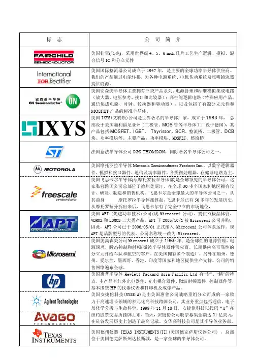
著名芯片厂商标志和简介之1标 志 公 司 简 介美国仙童(飞兆),采用世界级 4、5、6-inch 硅片工艺生产逻辑、模拟、混 合信号 IC 和分立元件 美国国际整流器公司成立于 1947 年,是主要的全球功率半导体供应商。
我们的产品通过电能转换,为各种电源系统、电机传动系统及照明镇流器 提供能源。
美国安森美半导体主要拥有三类产品系列: 电源管理和标准模拟集成电路 (放大器、电压参考、接口和比较器);高性能逻辑电路(特殊应用产品、 通信集成电路、时钟、转换器和驱动器);以及包括了有源分立元件和 MOSFET 产品的标准半导体。
IXYS美国 IXYS(艾赛斯)公司是世界著名的半导体厂家,成立于 1983 年, 总 部设于美国加利福尼亚州(二极管、MOS 管等半导体工厂设于德国) ,其 产品包括 MOSFET、IGBT、 Thyristor、SCR、整流桥、二极管、DCB 块、功率模块等。
主要产品:功率模块、MOSFET、整流桥 法国意法半导体公司 SGS-THOMSON,国际著名半导体公司之一。
美国摩托罗拉半导体 Motorola Semiconductor Products Inc.,以数字逻辑器 件、 模拟和接口器件、 通信及功率器件、 各类微处理器、 存储器电路为主。
美国飞思卡尔半导体(原摩托罗拉半导体部)是全球领先的半导体公司。
这 家私营跨国公司总部位于德州奥斯汀,在全球 30 多个国家和地区拥有设 计、研发、制造和销售机构。
飞思卡尔是全球最大的半导体公司之一。
从 其前身———摩托罗拉半导体部算起, 飞思卡尔已有 50 多年的发展历史, 从摩托罗拉分拆出来后,飞思卡尔有了完全中立的市场地位, 美国 APT (先进功率技术)公司(现 Microsemi 公司)。
提供双极晶体管、 VDMOS 和 LDMOS 三大类产品。
APT 于 2005/10/1 被 Microsemi 公司并购, 因此,APT 公司已于 2006/05/01 正式纳入 Microsemi 公司体系运作。
进口网络安全芯片排名进口网络安全芯片是保护网络安全的重要组成部分,它可以用来防御网络攻击、保护用户数据的安全性以及保障网络通信的可靠性。
随着互联网的迅速发展,网络安全问题也日益凸显,进口网络安全芯片的需求量逐渐增加。
下面就来介绍一下目前市场上几款知名的进口网络安全芯片。
1. 飞思卡尔(Freescale)Kinetis K61飞思卡尔公司是一家专门从事半导体产品研发的公司,在网络安全芯片领域具有较高的知名度。
Kinetis K61是飞思卡尔公司开发的一款高性能网络安全芯片,它采用了ARM Cortex-M4内核,具有优秀的处理性能和低功耗特性。
该芯片还支持多种安全功能,例如数据加密和身份验证等,能够有效地保护网络通信的安全性。
2. 英特尔(Intel)SGX英特尔公司是全球领先的半导体芯片制造商,其安全芯片技术在网络安全领域也有着广泛的应用。
Intel SGX(Software Guard Extensions)是一种支持硬件加密的安全芯片技术,它可以将软件运行在受保护的内存区域中,防止恶意软件的攻击和数据泄露。
SGX是一种非常理想的网络安全解决方案,目前已经广泛应用在云计算、物联网等领域。
3. 英飞凌(Infineon)OPTIGA TPM英飞凌公司是一家专门从事半导体和系统解决方案研发的公司,其网络安全芯片产品在市场上具有较高的声誉。
OPTIGA TPM 是英飞凌公司开发的一款安全芯片,它采用了可信平台模块(Trusted Platform Module,TPM)标准,可以为计算机和物联网设备提供可靠的安全认证和数据保护。
OPTIGA TPM芯片具有高度的安全性和可靠性,被广泛应用在金融、电子政务等领域。
4. STMicroelectronics ST33STMicroelectronics是一家全球领先的半导体解决方案供应商,其网络安全芯片产品也在行业内享有良好的声誉。
ST33是STMicroelectronics公司开发的一款安全芯片,它采用了ARM® SecurCore® SC300内核,具有出色的运算性能和安全性能。

飞思卡尔芯片飞思卡尔(Freescale)是一家拥有嵌入式半导体解决方案的全球领先制造商。
该公司的产品覆盖了自动驾驶汽车、智能手机、物联网以及工业自动化等领域。
飞思卡尔芯片是该公司的核心产品之一,下面将对其进行详细介绍。
飞思卡尔芯片是一种用于嵌入式系统的半导体芯片,具有高性能、低能耗的特点。
它可以运行复杂的应用程序,并提供丰富的外设接口,以满足各种设备的需求。
飞思卡尔芯片使用先进的制造工艺,具有较高的集成度和稳定性,同时还具有较低的功耗和散热性能。
飞思卡尔芯片提供了多种型号和系列,以满足不同应用场景的需求。
例如,i.MX系列是用于智能手机和平板电脑等移动设备的芯片,具有高性能、低功耗和丰富的多媒体功能。
QorIQ系列则是用于工业和网络设备的芯片,具有高性能、可靠性和安全性。
飞思卡尔芯片的应用范围非常广泛。
在汽车行业,它可以用于自动驾驶系统、车载娱乐系统和车身控制系统等。
在消费电子行业,它可以用于智能手机、平板电脑和智能家居设备等。
在工业自动化领域,它可以用于工业机器人、智能仓储系统和智能制造设备等。
与传统的微控制器相比,飞思卡尔芯片具有更强大的计算能力和更丰富的外设接口。
它可以支持更复杂的算法和应用程序,并且可以实现更高的系统集成度。
此外,飞思卡尔芯片还具有较低的功耗和散热性能,能够降低系统的能耗和散热压力。
飞思卡尔芯片还提供了丰富的软件和开发工具,以便开发人员快速开发和调试嵌入式系统。
它支持多种操作系统和开发环境,如Linux、Android和Microcontroller等。
同时,飞思卡尔芯片还提供了可靠的技术支持和培训,以帮助客户解决技术和应用问题。
总之,飞思卡尔芯片是一种用于嵌入式系统的半导体芯片,具有高性能、低能耗和丰富的外设接口。
它可以满足各种设备的需求,在多个行业具有广泛的应用前景。
随着物联网和智能制造技术的发展,飞思卡尔芯片将为各种智能设备的发展提供强大的支持。
hef40106bt芯片工作原理Hef40106bt芯片是一种六反相器化器,并且是由飞思卡尔公司(Freescale)制造的。
它由6个反相器组成,它们可以将输入信号从高电平转换为低电平,或从低电平转换为高电平。
hef40106bt芯片工作原理如下:1. 引脚功能:hef40106bt芯片一共有14个引脚,分别是VCC(正电源),GND(地),以及6个反相器输入引脚A1,A2,A3,A4,A5和A6;以及6个反相器输出引脚B1,B2,B3,B4,B5和B6。
2. 输入和输出特性:每个反相器都有一个输入和一个输出引脚。
当输入引脚接收到高电平时,输出引脚会变为低电平;当输入引脚接收到低电平时,输出引脚会变为高电平。
因此,hef40106bt芯片的主要功能是将输入信号进行反相处理。
3. 功能特点:每个反相器都具有相同的工作原理和特点。
当输入引脚接收到高电平时,输入端和反馈端之间的集电极结就会导通,输出引脚变为低电平,同时电容器开始充电。
当输入引脚接收到低电平时,反馈端和电源之间的集电极结导通,输出引脚变为高电平,电容器开始放电。
这种充电和放电的过程会导致输入信号的相反反馈。
4. 应用:hef40106bt芯片广泛应用于不同的电子电路中,尤其是在模拟信号处理和数字信号处理领域。
它可以用作振荡器、时钟发生器、信号放大器和滤波器等。
5. 注意事项:在使用hef40106bt芯片时需要注意以下几点:- 输入信号的幅值必须在芯片的供电范围之内,通常为0V到VCC之间。
- 要避免输入信号的幅值超过芯片的最大额定值,以防止芯片损坏。
- 输入和输出引脚之间应正确连接,以确保正确的信号传输。
- 在设计电路时,要合理选择适当的电容器和电阻器,以满足所需的工作条件和性能指标。
综上所述,hef40106bt芯片是一种用于信号反相处理的六反相器化器。
它通过充电和放电的过程将输入信号从高电平转换为低电平或从低电平转换为高电平。
在实际应用中,我们需要根据具体需求选择合适的输入信号幅值范围,正确连接引脚,并合理设计电路,以确保芯片的正常工作和性能。
1Kinetis E seriesKinetis E series provide the highly scalable portfolio ofARM ® Cortex ®-M0+ MCUs in the industry. With 2.7–5.5 V supply and focus on exceptional EMC/ESD robustness,Kinetis E series devices are well suited to a wide range of applications in electrical harsh environments, and is optimized for cost-sensitive applications offering low pin-count option.The Kinetis E series offers a broad range of memory,peripherals, and package options. They share common peripherals and pin counts allowing developers to migrate easily within an MCU family or among the MCU families to take advantage of more memory or feature integration. This scalability allows developers to standardize on the Kinetis E series for their end product platforms, maximising hardware and software reuse and reducing time-to-market.Following are the general features of the Kinetis E series MCUs.•32-bit ARM Cortex-M0+ core•Scalable memory footprints from 8 KB flash / 1 KB SRAM to 128 KB flash / 16 KB SRAM•Precision mixed-signal capability with on chip analog comparator and 12-bit ADC•Powerful timers for a broad range of applications including motor control•Serial communication interfaces such as UART, SPI,I 2C, and others.•High security and safety with internal watchdog andprogrammable CRC moduleProduct BriefRev 3, 07/2013KE02 Product BriefSupports all KE02 devices© 2013 Freescale Semiconductor, Inc.Contents1Kinetis E series..........................................................12KE02 sub-family introduction..................................23Block diagram...........................................................34Features.....................................................................45Power modes.. (136)Revision history (14)•Single power supply (2.7–5.5 V) with full functional flash program/erase/read operations•Ambient operation temperature range: –40 °C ~ 105 °CKinetis E series MCU families are supported by a market-leading enablement bundle from Freescale and numerous ARM third-party ecosystem partners. The KE02 sub-family is the entry-point to the Kinetis E series and is pin-compatible within E series and with the Freescale's 8-bit S08P family.2KE02 sub-family introductionThis sub-family includes a powerful array of analog, communication, and timing and control peripherals with specific flash memory size and the pin count.•Core and architecture:•ARM Cortex-M0+ core running up to 20 MHz with zero wait state execution from memories•Single-cycle access to I/O: Up to 50 percent faster than standard I/O, improves reaction time to externalevents allowing bit manipulation and software protocol emulation•Two-stage pipeline: Reduced number of cycles per instruction (CPI), enabling faster branch instruction andISR entry, and reducing power consumption•Excellent code density in comparison to 8-bit and 16-bit MCUs: Reduced flash size, system cost, andpower consumption•Optimized access to program memory: Accesses on alternate cycles reduces power consumption•100 percent compatible with ARM Cortex-M0 and a subset ARM Cortex-M3/M4: Reuse existingcompilers and debug tools•Simplified architecture: 56 instructions and 17 registers enable easy programming and efficient packagingof 8/16/32-bit data in memory•Linear 4 GB address space removes the need for paging/banking, reducing software complexity•ARM third-party ecosystem support: Software and tools to help minimize development time/cost •Bus clock running up to 20 MHz•BME: Bit manipulation engine reduces code size and cycles for bit-oriented operations to peripheral registerseliminating traditional methods where the core would need to perform read-modify-write operations.•Power-saving:•Low-power ARM Cortex-M0+ core with excellent energy efficiency•Supports three power modes: Run, Wait and Stop•Supports clock gating for unused modules, and specific peripherals remain working in Stop mode •Memory:•Up to 64 KB program flash, 256 B EEPROM, 4 KB SRAM•Embedded 32 B flash cache for optimizing bus bandwidth and flash execution performance •Mixed-signal analog:•Up to 16 channels of 12-bit analog-to-digital conversion (ADC) with 2.5 µs conversion time, 1.7 mV/°Ctemperature sensor, internal bandgap reference channel, supporting automatic compare, optional hardwaretrigger, and operating in Stop mode•Up to two analog comparators (ACMP) with both positive and negative inputs, separately selectable interrupt onrising and falling comparator output•Human-machine interface (HMI):•Up to two keyboard interrupt modules (KBI)•Connectivity and communications:•Up to three serial communications interface (UART) modules with optional 13-bit break, full duplex non-returnto zero (NRZ) and LIN extension support•Up to two serial peripheral interface (SPI) modules with full-duplex or single-wire bidirectional and master orslave mode•One Inter-integrated circuit ( I2C) module with bit rate up to 100 kbit/s, support system management bus •Reliability, safety and security:•Internal watchdog with independent clock source•Cyclic redundancy check (CRC) with programmable 16- or 32-bit polynomial generator•FlexTimer module (FTM) including one 6-channel FTM with deadtime insertion and fault detection, and up totwo 2-channel FTMs backward compatible with TPM modules. Each channel can be configured for inputcapture, output compare, edge- or center-aligned PWM mode.•Periodic interrupt timer (PIT) for RTOS task scheduler time base or trigger source for ADC conversion and timer modules•16-bit real timer counter (RTC)•I/O and package:•Up to 57 GPIO pins with interrupt functionality•Up to 2 true open-drain output pins•Up to 8 ultra high current sink pins supporting 20 mA source/sink current•Multiple package options from 32-pin to 64-pinThe family acts as a low-power, high-robustness, and cost-effective microcontroller to provide developers an appropriate entry-level 32-bit solution. The family is next generation MCU solution with enhanced ESD/EMC performance for cost-sensitive, high-reliability devices applications used in high electrical noise environments.3Block diagramThe following figure shows a superset block diagram of the device. Other devices within the family have a subset of the features.Kinetis KE02 FamilyFigure 1. KE02 family block diagramFeatures4.1Feature summaryAll devices within the KE02 sub-family have a minimum of the following features.44.2Memory and package optionsThe following table summarizes the memory and package options for the KE02 family. All devices which share a common package are pin-for-pin compatible.4.3Part numbers and packagingQ KE## A FFF T PP CC (N)Qualification statusFamily Flash sizeTemperature range (°C)Speed (MHz)Package identifierTape and Reel (T&R)Key attributeFigure 2. Part numbers diagrams4.4KE02 family featuresThe following sections list the differences among the various devices available within the KE02 family.The features listed below each part number specify the maximum configuration available on that device. The signal multiplexing configuration determines which modules can be used simultaneously.4.4.1KE02 family features (20 MHz performance)4.5Module-by-module feature listThe following sections describe the high-level module features for the family's superset device. See KE02 family features (20 MHz performance) for differences among the subset devices.Core modules4.5.1.1ARM Cortex-M0+ core•Up to 20 MHz core frequency from 2.7 V to 5.5 V across temperature range of –40 °C to 105 °C •Supports up to 32 interrupt request sources•2-stage pipeline microarchitecture for reduced power consumption and improved architectural performance (cycles per instruction)•Binary compatible instruction set architecture with the Cortex-M0 core •Thumb instruction set combines high code density with 32-bit performance •Serial wire debug (SWD) reduces the number of pins required for debugging •Single cycle 32 bits by 32 bits multiply4.5.1.2Nested Vectored Interrupt Controller (NVIC)Following are the features of the NVIC module.•Up to 32 interrupt sources•Includes a single non-maskable interrupt4.5.1.3Asynchronous Wake-up Interrupt Controller (AWIC)The features of the AWIC module are given below.•Supports interrupt handling when system clocking is disabled in low-power modes•Takes over and emulates the NVIC behavior when correctly primed by the NVIC on entry to very deep sleep mode.• A rudimentary interrupt masking system with no prioritization logic signals for wake-up as soon as a non-masked interrupt is detected•Contains no programmer’s model visible state and is therefore invisible to end users of the device other than through the benefits of reduced power consumption while sleeping4.5.1.4Debug controller•2-pin serial wire debug (SWD) provides external debugger interfaceSystem modules4.5.2.1Power Management Control (PMC) unitThe features of the PMC module are listed below.•Separate digital (regulated) and analog (referenced to digital) supply outputs •Programmable power saving modes•No output supply decoupling capacitors required•Available wake-up from power saving modes via RTC and external inputs •Integrated power-on-reset (POR)•Integrated low voltage detect (LVD) with reset (brownout) capability •Selectable LVD trip points•Programmable low-voltage warning (LVW) interrupt capability •Buffered bandgap reference voltage output4.5.14.5.2•Factory programmed trim for bandgap and LVD • 1 kHz low-power oscillator (LPO)4.5.2.2Watchdog (WDOG) moduleThe features of the Watchdog module are described as follows.•Independent clock source input (independent from CPU/bus clock)•Choice between clock sources• 1 kHz internal low-power oscillator (LPOCLK)•Internal 32 kHz reference clock (ICSIRCLK)•External clock (OSCERCLK)•Bus clock4.5.2.3System clocksThe following clock sources can be used as system clocks.•System oscillator (OSC)—Loop-control pierce oscillator; crystal or ceramic resonator range of 31.25 to 39.0625 kHz (low-range mode) or 4-20 MHz (high-range mode)•Internal clock source (ICS)•Frequency-locked loop (FLL) controlled by internal or external reference•16 MHz~20 MHz FLL output•Internal reference clocks—Can be used as a clock source for the other on-chip peripherals•On-chip RC oscillator range of 31.25 to 39.0625 kHz oscillator with ±1% deviation across temperature range of 0 °C to 70 °C and ±1.5% deviation across across full temperature rangeMemories and memory interfaces4.5.3.1On-chip memory•20 MHz performance devices•Up to 64 KB flash memory •Up to 256 B EEPROM memory •Up to 4 KB SRAM•Security circuitry to prevent unauthorized access to RAM and flash contentsAnalog4.5.4.1Analog-to-Digital Converter (ADC)The features of the ADC module are given below.•Linear successive approximation algorithm with 8-, 10-, or 12-bit resolution•Up to 16 external analog inputs, external pin inputs, and 5 internal analog inputs including internal bandgap,temperature sensor, and references•Output formatted in 8-, 10-, or 12-bit right-justified unsigned format•Single or continuous conversion (automatic return to idle after single conversion)•Supports up to eight result FIFO with selectable FIFO depth 4.5.34.5.4•Conversion complete flag and interrupt•Input clock selectable from up to four sources•Operation in Wait or Stop modes for lower noise operation •Asynchronous clock source for lower noise operation •Selectable asynchronous hardware conversion trigger•Automatic compare with interrupt for less-than, or greater-than or equal-to, programmable value4.5.4.2Analog Comparator (ACMP)The ACMP module has the following features.•Operational over the whole supply range of 2.7–5.5 V•On-chip 6-bit resolution DAC with selectable reference voltage from V DD or internal bandgap •Configurable hysteresis•Selectable interrupt on rising-edge, falling-edge, or both rising or falling edges of the comparator output •Selectable inversion on comparator output•Up to four selectable comparator inputs; one of these is fixed and connected to built-in DAC output while the others are externally mapped on pinouts.•Operational in Stop modeTimer4.5.5.1FlexTimers (FTM)The FlexTimer module exhibits the following features.•Selectable FTM source clock •Programmable prescaler•16-bit counter supporting free-running or initial/final value, and counting is up or up-down •Input capture, output compare, and edge-aligned and center-aligned PWM modes •Input capture and output compare modes•Operation of FTM channels as pairs with equal outputs, pairs with complimentary outputs, or independent channels with independent outputs•Deadtime insertion is available for each complementary pair •Generation of hardware triggers •Software control of PWM outputs•Up to four fault inputs for global fault control •Configurable channel polarity•Programmable interrupt on input capture, reference compare, overflowed counter, or detected fault condition4.5.5.2Periodic Interrupt Timer (PIT)The features of the PIT module are given below.•Two general-purpose interrupt timers•One interrupt timer for triggering ADC conversions •32-bit counter resolution•Clocked by bus clock frequency4.5.5.3Real-Time Clock (RTC)Following are the features of the real-time clock.4.5.5•16-bit up-counter•16-bit modulo match limit•Software controllable periodic interrupt on match•Software selectable clock sources for input to prescaler with programmable 16 bit prescaler•OSC 32.678 kHz nominal •LPO (~1 kHz)•Bus clock•Internal reference clock (32 kHz)Communication interfaces4.5.6.1Inter-Integrated Circuit (I 2C)The features of the I 2C module are as follows.•Compatible with I 2C bus standard•Up to 100 kbit/s with maximum bus loading •Multimaster operation•Software programmable for one of 64 different serial clock frequencies •Programmable slave address and glitch input filter •Interrupt-driven byte-by-byte data transfer•Arbitration lost interrupt with automatic mode switching from master to slave •Calling address identification interrupt•Bus busy detection broadcast and 10-bit address extension•Address matching causes wake-up when processor is in low-power mode.4.5.6.2Universal Asynchronous Receiver/Transmitter (UART)The UART module has the following features.•Full-duplex, standard non-return-to-zero (NRZ) format•Double-buffered transmitter and receiver with separate enables •Programmable baud rates (13-bit modulo divider)•Interrupt-driven or polled operation:•Transmit data register empty and transmission complete •Receive data register full•Receive overrun, parity error, framing error, and noise error •Idle receiver detect•Active edge on receive pin •Break detect supporting LIN•Hardware parity generation and checking •Programmable 8-bit or 9-bit character length •Programmable 1-bit or 2-bit stop bits•Receiver wake-up by idle-line or address-mark•Optional 13-bit break character generation / 11-bit break character detection •Selectable transmitter output polarity4.5.6.3Serial Peripheral Interface (SPI)The features of the SPI module are listed below.•Master and slave mode•Full-duplex, three-wire synchronous transfers4.5.6•Programmable transmit bit rate•Double-buffered transmit and receive data registers •Serial clock phase and polarity options •Slave select output•Mode fault error flag with CPU interrupt capability •Control of SPI operation during Wait mode •Selectable MSB-first or LSB-first shifting •Receive data buffer hardware match featureHuman machine interface4.5.7.1General-Purpose Input/Output (GPIO)The features of the GPIO module are listed below.•Hysteresis and configurable pull up device on all input pins •Configurable drive strength on some output pins•Independent pin value register to read logic level on digital pin4.5.7.2Keyboard Interrupts (KBI)The KBI features include:•Up to eight keyboard interrupt pins with individual pin enable bits •Each keyboard interrupt pin is programmable as:•falling-edge sensitivity only •rising-edge sensitivity only•both falling-edge and low-level sensitivity •both rising-edge and high-level sensitivity •One software-enabled keyboard interrupt •Exit from low-power modes5Power modesThe power management controller (PMC) provides the user with multiple power options. The different modes of operation are supported to allow the user to optimize power consumption for the level of functionality needed.The device supports Run, Wait, and Stop modes which are easy to use for customers both from different power consumption level and functional requirement. I/O states are held in all the modes.•Run mode—CPU clocks can be run at full speed and the internal supply is fully regulated.•Wait mode—CPU shuts down to conserve power; system clocks and bus clock are running and full regulation is maintained.•Stop mode—LVD optional enabled, and voltage regulator is in standby.The three modes of operation are Run, Wait, and Stop. The WFI instruction invokes both Wait and Stop modes for the chip.4.5.76Revision historyThe following table provides a revision history for this document.How to Reach Us: Home Page: Web Support: /support Information in this document is provided solely to enable system and software implementers to use Freescale products. There are no express or implied copyright licenses granted hereunder to design or fabricate any integrated circuits based on the information in this document. Freescale reserves the right to make changes without further notice to any products herein.Freescale makes no warranty, representation, or guarantee regarding the suitability of its products for any particular purpose, nor does Freescale assume any liability arising out of the application or use of any product or circuit, and specifically disclaims any and all liability, including without limitation consequential or incidental damages.“Typical” parameters that may be provided in Freescale data sheets and/or specifications can and do vary in different applications, and actual performance may vary over time. All operating parameters, including “typicals,” must be validated for each customer application by customer's technical experts. Freescale does not convey any license under its patent rights nor the rights of others. Freescale sells products pursuant to standard terms and conditions of sale, which can be found at the following address: /SalesTermsandConditions. Freescale, the Freescale logo, and Kinetis are trademarks of Freescale Semiconductor, Inc., Reg. U.S. Pat. & Tm. Off. All other product or service names are the property of their respective owners. ARM and Cortex-M0+ are the registered trademarks of ARM Limited.©2013 Freescale Semiconductor, Inc.Document Number KE02PBRevision 3, 07/2013。


飞思卡尔i.MX27芯片介绍飞思卡尔是MP4方案中率先支持RMVB格式的视频解码方案,为产品的拓展,开辟了新的思路。
将视频编解码功能嵌入到多媒体应用处理器中已经成为一个趋 势。
飞思卡尔半导体DragonBall家族的最新成员i.MX27多媒体应用处理器,片内集成H.264/MPEG4全双工硬件编解码视频处理单元,是 嵌入式多媒体应用处理器的一颗新星,可广泛应用于视频监控、网络摄像机、数字录像机、网络广告机、V2IP可视电话、IPTV机顶盒、智能手机、便携式多 媒体播放器、移动电视等产品。
MX27处理器以MX21为基础进行设计,基于ARM926EJ-S。
处理器内部的硬件编解码模块性能强劲,可以达到H.264/MPEG4编解码D1分 辨率:720X576、25fps和720x480、30fps;全双工编解码同时进行可以达到VGA分辨率:640x480、30fps,在目前的嵌入 式ARM处理器中鲜有敌手。
而且,MX27可以同时进行H.264VGA、30fps的编码和MPEG4 VGA、30fps的解码;也能MPEG4VGA、30fps编码和H.264 VGA、30fps解码同时进行。
MX27支持多方网络视频会议和多种视频格式编解码:H.264/A VC baseline profile encoding/decoding;MPEG-4 part-II simple profile encoding/decoding;H.263 P3 encoding/decoding;多方会议:最多可同时处理4路图像/位流的编解码;全双工多格式支持:在做MPEG4编码的同时可以做H.264的解码;支持码率控制,支持CBR和VBR。
和某些含视频编解码功能的嵌入式处理器相比,MX27的硬件编解码是通过CPU内部ASIC实现的,而不是通过集成ARM和DSP的双核SOC实现。
因此,MX27的功耗更低,系统整体性能更强。
MX27处理器还带有eMMA多媒体加速器模块,包括prp预处理和pp后处理两部分,用来进行图像的缩放、旋转、镜像、YUV/RGB数据转换等。
DSP的产生和发展世界上第一片DSP芯片是1978年AMI公司的S2811,1979年美国Intel公司宣布生产的商用可编程器件2920是DSP芯片的一个主要标志。
但是,这两种芯片内部都没有现代DSP芯片所必须的单周期乘法器。
1980年,日本NEC公司推出的μPD7720是第一片具有硬件乘法器的商用DSP芯片。
美国德州仪器公司(TI公司)在1982年成功推出其第一代DSP 芯片TMS32010及其系列产品。
第一个采用CMOS工艺生产浮点DSP芯片的是日本的日立(Hitachi)公司,该公司于1982年推出了浮点DSP芯片。
而第一片高性能的浮点DSP芯片是AT&T公司于1984年推出的DSP32。
飞思卡尔(Freescale)公司的前身摩托罗拉公司半导体部,1986年推出了定点处理器MC56001。
1990年推出了与IEEE浮点格式兼容的浮点DSP芯片MC96002。
到2005年,飞思卡尔公司推出了56F8300系列的定点DSP,如56F83367、56F8334等。
美国模拟器件公司(Analog Devices, 简称AD)也相继推出了一系列具有自己特点的DSP 芯片,其定点DSP 芯片有ADSP2101/2103/2105 、ASDP2111/2115 、ADSP2161/2162/2164 以及ADSP2171/2181 等。
经过30多年的不断技术创新,DSP芯片得到了突飞猛进的发展,主要表现在以下几个方面:(1) 制造工艺不断提高。
(2) 片内存储器容量不断加大。
(3) 内部结构日益完善,片内外设接口不断丰富。
(4) 处理速度不断加快。
(5) 运算精度不断提高。
(6) 开发工具更加智能化,功能也日益强大。
DSP处理器的结构和特点为了实现高速数字信号处理以及实时地进行系统控制,DSP芯片一般都采用了不同于通用CPU和MCU的特殊软硬件结构。
尽管不同公司的DSP其结构不尽相同,但是在处理器结构、指令系统等方面有许多共同点。
MC56F827xx快速上手指南作者:傅志强飞思卡尔半导体(中国)有限公司目录1.芯片简介: (2)2.开发工具: (3)2.1.硬件工具: (3)2.2.软件工具: (3)3.手册资料: (4)3.1.芯片资料: (4)3.2.开发工具手册: (5)3.3.例程: (5)4.CodeWarrior使用简介: (5)4.1.创建新工程: (5)4.2.编辑代码: (8)4.3.编译和下载、调试: (9)5.C语言编程要点: (11)5.1.整数和小数: (11)5.2.使用编译器自带的函数: (12)5.3.使用嵌入式软件库中的数学函数: (13)5.3.1.添加嵌入式软件库到工程中: (13)5.3.2.调用嵌入式软件库中的函数: (15)5.4.中断服务程序和向量表: (16)6.片内模块驱动程序编程: (17)6.1.如何阅读芯片的手册: (17)6.2.系统时钟配置: (18)6.3.外设模块初始化一般流程: (20)1.芯片简介:MC56F827xx/3xx是一款低功耗数字信号控制器(DSC)系列产品,在运行时功耗极低。
它采用紧凑型5x5 mm封装,具有优异的性能、精度和控制特性,适用于高效数字电源转换(MC56F827xx)和高级电机控制(MC56F823xx)应用。
它的主要特点有:50/100 MHz 32位DSP内核可为高级电源和电机控制等应用提供所需的数学运算功能。
支持单周期数学运算、小数运算和并行移动,可提高性能,实现更紧凑、更快的控制回路PWM带死区时间插入和紧急关闭功能,分辨率高达312皮秒,可实现更高的切换频率,降低了成本并提高了效率。
两个12位高速ADC,内置PGA,采样率高达1.25 MSPS,可以同时采样以提高系统精度。
直接存储器存取(DMA)控制器可减少内核中断,增强系统性能。
4个模拟比较器,内置6位数模转换器(DAC),可实现高速系统事件识别和PWM输出紧急关闭功能。
飞思卡尔半导体产品概述文档号: K10PBZHS 第2版, 2010年11月目录1Kinetis 产品组合Kinetis 是基于ARM® Cortex TM-M4具有超强可扩展性的低功耗、混合信号微控制器。
第一阶段产品由五个微控制器系列组成,包含超过两百种器件,在引脚、外设和软件上可兼容。
每个系列提供了不同的性能,存储器和外设特性。
通过通用外设、存储器映射和封装的一致性来实现系列内和各系列间的便捷移植。
Kinetis 微控制器基于飞思卡尔创新的90 纳米薄膜存储器(TFS)闪存技术,具有独特的Flex存储器(可配置的内嵌EEPROM)。
Kinetis 微控制器系列融合了最新的低功耗革新技术,具有高性能、高精度的混合信号能力,宽广的互连性,人机接口和安全外设。
飞思卡尔公司以及其他大量的ARM第三方应用商提供对Kinetis 微控制器的应用支持。
1Kinetis 产品组合 . . . . . . . . . . . . . . . . . 1 2K10系列介绍. . . . . . . . . . . . . . . . . . . 4 3K10模块结构图. . . . . . . . . . . . . . . . . . 4 4特性. . . . . . . . . . . . . . . . . . . . . . . 64.1K10系列MCU的共性. . . . . . . . . . . . . 64.2Flex存储器 . . . . . . . . . . . . . . . . . 74.3器件号和封装信息 . . . . . . . . . . . . . . 84.4K10系列特性 . . . . . . . . . . . . . . . 104.5模块特性 . . . . . . . . . . . . . . . . . 27 5功耗模式. . . . . . . . . . . . . . . . . . . . 37 6开发环境. . . . . . . . . . . . . . . . . . . . 386.1飞思卡尔的塔式系统 . . . . . . . . . . . . 386.2CodeWarrior开发组件 . . . . . . . . . . . 396.3飞思卡尔的MQX TM软件解决方案 . . . . . . 406.4额外提供的软件栈 . . . . . . . . . . . . . 42 7修订记录. . . . . . . . . . . . . . . . . . . . 42K10系列产品概述适用于所有K10微控制器Kinetis 产品组合图 1. Kenetis微控制器产品组合所有的 Kinetis系列包含丰富的模拟、通信和定时控制外设,提供多种闪存容量和输入输出引脚数量。
飞思卡尔9S12系列单片机中文简介1.1介绍MC9S12G系列是一个专注于低功耗、高性能、低引脚数量的高效汽车级16位微控制器产品。
这个系列是桥连8位高端微机和16位高性能微机,像MC9S12XS系列。
MC9S12G系列是为了满足通用汽车CAN或LIN/J2602通信应用。
这些应用的典型例子包括body controllers, occupant detection, door modules, seat controllers, RKE receivers, smart actuators, lighting modules, and smart junction boxes.MC9S12G系列使用了许多MC9S12XS系列和MC9S12P系列里面的相同特性,包括在闪存(flash memory)上的纠错指令(ECC),一个快速A/D转换器(ADC)和一个为了改善电磁兼容性(EMC)性能的频率调制相位锁存循环(IPLL).MC9S12G系列是高效的对较低的程序存储器至16K。
为了简化顾客使用它,特制了一个4字节可擦除扇区的EEPROM。
MC9S12G系列传送所有16位单片机的优势和效率,定位于低成本,低功耗,EMC,现行代码尺寸效率优势被现存8位和16位单片机系列的使用者所分享。
像MC9S12XS系列,MC9S12G 系列运行16位位宽的访问对所有的周期和存储器状态都不用等待。
MC9S12G系列可得到的封装有100-pin LQFP, 64-pin LQFP, 48-pin LQFP/QFN, 32-pin LQFP and 20-pin TSSOP,特别是对较少引脚的封装发挥出最大的功能。
此外,在每个模块中可得到的I/O口,进一步的可用于中断的I/O口允许从停止或等待模式中唤醒。
1.2特点这部分说明了MC9S12G系列的关键特性。
1.2.1MC9S12G系列比较表1-1提供了MC9S12G系列不同型号特点的概要。