orcad pspice 仿真教程 1
- 格式:ppt
- 大小:369.00 KB
- 文档页数:14


Orcad使用教程1第一章概论本章在简要介绍计算机辅助设计(CAD: Computer Aided Design)和电子设计自动化(EDA: Electronic Design Automation)基本概念的基础上,介绍OrCAD/PSpice软件的功能和特点,并具体说明调用PSpice软件进行电路模拟的基本步骤。
1-1 EDA技术和PSpice软件1-1-1 CAD和EDA进行电子线路设计,就是根据给定的设计要求,包括功能和特性指标要求,通过各种方法,确定应采用什么样的线路拓扑结构以及线路中各个元器件应采用什么参数值。
有时还需将设计好的线路进一步转换为印刷电路板版图设计。
要完成上述设计任务,一般需经过设计方案提出、验证和修改(若需要的话)三个阶段,有时甚至要经历几个反复,才能完成一个比较好的电路设计。
按照上述三个阶段中完成任务的手段不同,可将电子线路的设计方式分为不同类型。
如果方案的提出、验证和修改都是人工完成的,则称之为人工数字电路激励信号源J 结型场效应晶体管(JFET) V 独立电压源K 互感(磁芯),传输线耦合 W 电流控制开关L 电感 X 单元子电路调用M MOS场效应晶体管(MOSFET) Z 绝缘栅双极晶体管(IGBT)注:表中N器件和O器件是在数/模混合电路中对数/模接口型节点进行接口电路转换时引进的两种等效器件,详见第八章。
2. 元器件模型电路模拟的精度很大程度上取决于电路中代表各种元器件特性的模型参数值是否精确。
为了方便用户使用,PSpice A/D提供的模型参数库中包括有超过11300种的半导体器件和模拟集成电路产品的模型参数,以及1600多种数字电路单元产品的参数。
其中不但包括了最新的GaAs器件和IGBT器件模型参数,对MOSFET器件还提供了6种不同级别的模型,适用于先进的亚微米工艺器件。
第十章将介绍不同元器件模型参数的基本含义及其对电路特性模拟的影响。
在本书所附的光盘中,Document路径下的Analog和Digital两个文件分别列出了模型参数库中包括的模拟和数字两类元器件名称清单。
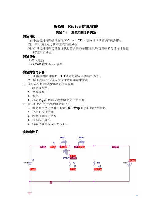
OrCAD PSpice仿真实验实验5.1 直流扫描分析实验实验目的:1)学会使用电路绘制程序在Capture CIS环境内绘制所需要的电路图.2)学习偏压点分析和直流扫描分析.3)练习使用电路仿真程序执行仿真并显示出波形,将仿真结果与理论计算值比较加以验证.实验设备:1)个人电脑2)OrCAD 9.2Release软件实验内容与步骤:1.听指导教师讲解OrCAD基本知识及基本操作方法.2.按下列操作步骤依次完成仿真和结果预测.1)偏压点分析并观察输出文件的内容.1.绘出电路图.2.设置参数.3.保存.4.启动Pspice仿真及观察输出文件的内容.2)直流扫描分析并观察输出波形1.调出原电路图文件并设置DC Sweep直流扫描分析参数.2.存档并执行仿真.3.观察仿真输出结果.4.打印输出波形.5.将输出波形存成图形文件.实验电路图:输出结果:**** INCLUDING wz___3-SCHEMA ***** source WZ___3V_V1 N00113 0 15VdcR_R1 N00113 N00143 12R_R2 0 N00207 10R_R3 0 N00157 40I_I1 N00157 0 DC 4AdcV_PRINT1 N00143 N00221 0V.PRINT DC I(V_PRINT1)V_PRINT2 N00221 N00157 0V.PRINT DC I(V_PRINT2)V_PRINT3 N00207 N00221 0V.PRINT DC I(V_PRINT3)NODE VOL TAGE NODE VOL TAGE NODE VOL TAGE NODE VO L TAGE(N00113) 15.0000 (N00143) -13.2000 (N00157) -13.2000 (N00207) -13.2000(N00221) -13.2000VOL TAGE SOURCE CURRENTSNAME CURRENTV_V1 -2.350E+00V_PRINT1 2.350E+00V_PRINT2 3.670E+00V_PRINT3 1.320E+00实验结果分析:I1=2.350A I2=3.670A I3=1.320AI2=I1+I3 所以结果符合叠加原理实验5.3 交流扫描分析实验实验目的:练习使用Pspice的交流扫描分析(AC sweep)功能,进行交流电路的分析计算,以及电路频率的特性分析.实验设备:1)个人电脑2)OrCAD 9.2Release软件实验内容与步骤:1)绘制电路图.设置参数:分析类型设置为交流扫描(AC sweep),并选择原始频率为1Hz,终止频率为100kHz,每十倍频程的扫描点数Points/decade设置为100.2)执行Pspice仿真完成后,自动进入图形处理界面.3)添加曲线命令.观察波形,打印输出波形.4)查看输出文件.实验电路图:输出图形:输出结果:V_V1 N01192 0 DC 0 AC 220V acR_R2 0 N01110 280L_L2 N01192 N01169 1.65V_PRINT1 N01169 N011430V.PRINT AC IM(V_PRINT1)R_R1 N01143 N01110 20NODE VOL TAGE NODE VOL TAGE NODE VO L TAGE NODE VOL TAGE (N01110) 0.0000 (N01143) 0.0000 (N01169) 0.0000 (N01192) 0.0000VOL TAGE SOURCE CURRENTSNAME CURRENTV_V1 0.000E+00V_PRINT1 0.000E+00TOTAL POWER DISSIPA TION 0.00E+00 W A TTS。


OrCAD/PSpice9的电路仿真方法1、概 述1.1 PSpice 软件P S p i c e是一个电路通用分析程序,是E D A中的重要组成部分,它的主要任务是对电路进行模拟和仿真。
该软件的前身是S P I C E(S i m u l a t i o n P r o g r a m w i t h I n t e g r a t e d C i r c u i t E m p h a s i s),由美国加州大学伯克莱分校于1972年研制。
1975年推出正式实用化版本S P I C E2G,1988年被定为美国国家标准。
1984年M i c r o s i m公司推出了基于S P I C E的微机版本P S p i c e (P e r s o n a l-S P I C E),此后各种版本的S P I C E不断问世,功能也越来越强。
进入20世纪90年代,随着计算机软件的飞速发展,特别是W i n d o w s操作系统的广泛流行,P S p i c e又出现了可在W i n d o w s环境下运行的5.1、6.1、6.2、8.0等版本,也称为窗口版,采用图形输入方式,操作界面更加直观,分析功能更强,元器件参数库及宏模型库也更加丰富。
1998年1月,著名的E D A公司O r C A D公司与开发P S p i c e软件的M i c r o s i m公司实现了强强联合,于1998年11月推出了最新版本O r C A D/P S p i c e9。
为了迅速推广普及O r C A D/P S p i c e9软件,O r C A D公司提供了一张试用光盘O r C A D/P S p i c e 9D e m o, 它与商业版是完全一致的,不同之处只是在元器件上受到一定的限制,因此又被称为普及版。
本章将以普及版为例简要介绍O r C A D/P S p i c e9的功能及使用方法。
本书中所有的虚拟实验都是用O r C A D/P S p i c e9D e m o完成的,所引用的屏幕画面也都是出自于O r C A D/P S p i c e 9D e m o软件。

电路原理仿真练习OrCAD/PSpice软件使用方法简介一、直流电阻电路的仿真直流仿真包括直流工作点(bias point)、直流扫描(DC sweep)和灵敏度(sensitivity)分析。
以OrCAD Demo 9.0为例,仿真步骤如下:1.运行Capture CIS Demo。
2.创建新项目(Project)。
执行File\New\Project,出现“New Project”对话框。
在“Name”处输入设计项目名称;中间的四个选项中点击选中“Analog or Mixed-Signal Ciecuit”;在“Location”处指定项目有关文件所放路径;点击Ok,出现“Analog Mixed-Mode Project Wizard”对话框。
3.添加元件库。
在2中出现的对话框中,用鼠标左键双击左边方框中要用到的元件库名(或先用鼠标选中元件库名,再按Add),则该元件库名出现在右边方框内;按完成按钮。
即出现电路图绘制窗口Schematic。
4.放置元件。
点击Place\Part,出现“Place Part”对话框;在“Libraries”下面方框中选择所要用的元件库。
R, L, C元件及受控源在Analog库中,独立源在Source 库中。
独立电压源元件以V开头,独立电流源元件以I开头,例VDC表示直流电压源,IAC表示交流电流源等。
在Libraries上面的方框中选中元件,按OK,元件就会出现在绘图窗口,按鼠标左键即可将元件放置在所需位置。
若还需再加该种元件,则可再按鼠标左键放置即可。
若要结束该种元件的放置,则按鼠标右键,选“End Mode”。
其它元件可按同样方法绘制。
激活元件按鼠标右键选“rotate”可改变元件方向。
5.设置元件参数。
每个电路元件均有默认值,元件放置后可根据要仿真的的电路设置其参数。
像RLC元件和直流电源,可直接用鼠标点击元件一侧的元件值,在对话框中输入元件值即可。

在O r CAD/PSpice 9.2平台上电子电路设计与仿真Pspice实践练习一:设计与仿真一个单级共射放大电路(提供的参考电路如图一所示)。
要求:放大电路有合适静态工作点、电压放大倍数30左右、输入阻抗大于1KΩ、输出阻抗小于5.1KΩ及通频带大于1MHZ 。
请参照下列方法及步骤,自学完成Pspice实践练习一。
一、启动Pspice9.2 →Capture →在主页下创建一个工程项目exa1。
⒈选File/New/ Project⒉建立一个子目录→Create Dir (键入e:\zhu),并双击、打开子目录;⒊选中●Analog or Mixed- Signal Circuit OK!⒋键入工程项目名exa1;⒌在设计项目创建方式选择对话下,选中●Create a blank pro OK!⒍画一直线,将建立空白的图形文件(exa1.sch)存盘。
二、画电路图(以单级共射放大电路为例,电路如图一所示)⒈打开库浏览器选择菜单Place/Part → Add Library提取:三极管Q2N2222(bipolar库)、电阻R、电容C(analog库)、电源VDC(source库)、模拟地0/Source、信号源VSIN。
⒉移动元、器件。
鼠标选中元、器件并单击(元、器件符号变为红色),然后压住鼠标左键拖到合适位置,放开鼠标左键即可。
⒊删除某一元、器件。
鼠标选中该元、器件并单击(元、器件符号变为红色),选择菜单Edit/delete 。
⒋翻转或旋转某一元、器件符号。
鼠标选中该元、器件并单击(元、器件符号变为红色),可按键Ctrl +R 即可。
⒌画电路连线选择菜单中Place/wire,此时将鼠标箭头变成为一支笔(自己体会)。
⒍为了突出输出端,需要键入标注Vo 字符,选择菜单Place/Net Alias → Vo OK!三、修改元、器件的标号和参数⒈.用鼠标箭头双击该元件符号(R 或C),此时出现修改框,即可进入标号和参数的设置。

OrCAD Flow Tutorial, Product Version 16.02Creating a schematic designThis chapter consists of the following sections:ObjectiveDesign exampleCreating a design in CaptureProcessing a designSummaryWhat's nextRecommended readingObjectiveTo create a schematic design in OrCAD Capture. In this chapter, you will be introduced to basic design steps, such as placing a part, connecting parts using wires, adding ports, generating parts, and so on.The steps for preparing your design for simulation using PSpice and for taking your design for placement and routing to OrCAD Layout or OrCAD PCB Editor are also covered in this chapter.Design exampleIn this chapter, you will create a full adder design in OrCAD Capture. The full adder design covered in this tutorial is a complex hierarchical design that has two hierarchical blocks referringto the same half adder design.Duration:40 minutesCreating a design in CaptureGuidelinesWhen creating a new circuit design in OrCAD Capture, it is recommended that you follow the guidelines listed below.1.Avoid spaces in pathnames and filenames. This is necessary to get your design intodownstream products, such as SPECCTRA for OrCAD.2.Avoid using special characters for naming nets, nodes, projects, or libraries. While namingnets, use of illegal characters listed below might cause the netlister to fail.? (question mark)@ (at symbol)~ (telda)#(hash)& (ampersand)% (percent sign)" (quotation marks)! (exclamation mark)( )(parenthesis)< (smaller than)= (equal)> (greater than)[ ](square parenthesis),* (asterisk)Creating a projectTo create a new project, we will use Capture's Project Wizard. The Project Wizard provides you with the framework for creating any kind of project.unch Capture.2.From the File menu, choose New > Project.3.In the New Project dialog box, specify the project name as FullAdd.4.To specify the project type, select Analog or Mixed A/D.Note: An Analog or Mixed A/D project can easily be simulated using PSpice. It alsoensures that your design flows smoothly into OrCAD Layout for your board design.5.Specify the location where you want the project files to be created and click OK.6.In the Create PSpice Project dialog box, select the Create a blank project option button.Note: When you create a blank project, the project can be simulated in PSpice, butlibraries are not configured by default. When you base your project on an existing project, the new project has same configured libraries.7.Click OK to create the FullAdd project with the above specifications.In case you already have a schematic design file (.dsn) that you want tosimulate using PSpice, you need to create an Analog or Mixed A/D project usingthe File > New > Project command and then add your design to it.The FullAdd project is created. In the Project Manager window, a design file, fulladd.dsn, is created. Below the design file, a schematic folder with the name SCHEMATIC1 is created. This folder has a schematic page named PAGE1.Renaming the schematic folder and the schematic pageYou will now modify the design to change the name of both the schematic folder and the schematic page, to HALFADD.1.In the Project Manager window, right-click on SCHEMA TIC1.2.From the pop-up menu, select Rename.3.In the Rename Schematic dialog box, specify the name as HALFADD.4.Similarly, right-click on PAGE1 and from the pop-up menu select Rename.5.In the Rename Page dialog box, specify the page name as HALFADD and click OK. After renaming of the schematic folder and the schematic page, the directory structure in the Project Manager window should be to similar to the figure below.Using a design templateBefore you start with the design creation process in OrCAD Capture, you can specify the default characteristics of your project using the design template. A design template can be used to specify default fonts, page size, title block, grid references and so on. To set up a design template in OrCAD Capture, use the Design Template dialog box.- To open the Design Template dialog box, from the Options drop-down menu choose Design Template.To know more about setting up the design template, see OrCAD Capture User's Guide. Creating a flat designIn this section, we will create a simple flat half adder design with X and Y as inputs and SUM and CARRY as outputs.Adding partsTo add parts to your design:1.From the Place menu in Capture, select Part.2.In the Place Part dialog box, first select the library from which the part is to be added andthen instantiate the part on the schematic page.The gates shown in Figure 2-1 are available in the 7400.OLB.Use the Part Search button in the Place Part dialog box, to search the library towhich the required part belongs.To add 7400.OLB to the project, select the Add Library button.3.Browse to <install_dir>/tools/capture/library/pspice/7400.olb.Select 7400.OLB and click Open.The 7400 library appears in the Libraries list box.4.From the Part List, select 7408 and click OK.5.Place three instances of the AND gate, 7408, on the schematic page as shown in the figure below.6.Right-click and select End Mode.7.Similarly, place an OR gate (7432) and two NOT gates (7404) as shown in the figurebelow.Connecting partsAfter placing the required parts on the schematic page, you need to connect the parts.1.From the Place menu, choose Wire.The pointer changes to a crosshair.2.Draw the wire from the output of the AND gate, U2A, to the one of the inputs of the ORgate, U1B. To start drawing the wire, click the connection point of the output pin, pin3, on the AND gate.3.Drag the cursor to input pin, pin4, of the OR gate (7432) and click on the pin to end thewire.Clicking on any valid connection point ends a wire.4.Similarly, add wires to the design until all parts are connected as shown in the figurebelow.5.To stop wiring, right-click and select End Wire. The pointer changes to the default arrow. Adding portsTo add input and output ports to the design, complete the following sequence of steps:1.From the Place menu in Capture, select Hierarchical Port.The Place Hierarchical Port dialog box appears.Note: Alternatively, you can select the Place port button from the Tool Palette.2.From the Libraries list box, select CAPSYM.3.First add input ports. From the Symbols list, select PORTRIGHT-R and click OK.4.Place two instances of the port as shown in the figure below5.Right-click and select End Mode.6.To rename the ports to indicate input signals X and Y, double-click the port name.7.In the Display Properties dialog box, change the value of the Name property to X and clickOK.Note: You can also use the Property Editor to edit the property values of a component. To know the details, see OrCAD Capture User's Guide.8.Similarly, change the name of the second port to Y.Note: You cannot use the Place Part dialog box for placing ports, because ports inCAPSYM.OLB are only symbols and not parts. Only parts are listed in the Place Partdialog box.9.Add two output ports as shown in the figure below. To do this, select PORTLEFT-L fromthe CAPSYM library.10.Rename the ports to SUM and CARRY, respectively.11.Save the design.The half adder design is ready. The next step is to create a full adder design that will use the half adder design.Creating a hierarchical designIn Capture, you can create hierarchical designs using one of the following methods:Bottom-up methodTop-down methodAnother method of creating a hierarchical design is to create parts or symbols for the designs at the lowest level, and save the symbols in a user-defined library. You can later add the user-defined library in your projects and use these symbols in the schematic. For example, you can create a part for the half adder design and then instead of hierarchical blocks, use this part in the schematic. To know more about this approach, see Generating parts for a schematic.In this section, we will create the full adder hierarchical design. The half adder design created in the Creating a flat design section will be used as the lowest level design.Bottom-up methodWhen you create a hierarchical design using the bottom-up methodology, you need to follow these steps.Create the lowest-level design.Create higher-level designs that instantiate the lower-level designs in the form ofhierarchical blocks.In this section, we will create a full adder design using bottom-up methodology. The steps involved are:1.Creating a project in Capture. To view the steps, see Creating a project.2.Creating the lowest-level design. In the full adder design example, the lowest-level designis the half adder design. To go through the steps for creating the half adder design, seeCreating a flat design.3.Creating the higher-level design. Create a schematic for the full adder design that uses thehalf adder design created in the previous step. To go through the steps, see Creating thefull adder design.Creating the full adder design1.In the Project Manager window, right-click on fulladd.dsn and select New Schematic.2.In the New Schematic dialog box, specify the name of the new schematic folder asFULLADD and click OK.In the Project Manager window, the FULLADD folder appears below fulladd.dsn.3.Save the design.4.To make the full adder circuit as the root design (high-level design), right-click onFULLADD and from the pop-up menu select Make Root.The FULLADD folder moves up and a forward slash appears in the folder.5.Right-click on FULLADD and select New Page.6.In the New Page in schematic: FULLADD dialog box, specify the page name as FULLADD and click OK.A new page, FULLADD, gets added below the schematic folder FULLADD.7.Double-click the FULLADD page to open it for editing.8.From the Place menu, choose Hierarchical Block.9.In the Place Hierarchical Block dialog box, specify the reference as HALFADD_A1.10.Specify the Implementation Type as Schematic View.11.Specify the Implementation name as HALFADD and click OK.The cursor changes to a crosshair.12.Draw a rectangle on the schematic page.A hierarchical block with input and output ports is drawn on the page.13.If required, resize the block. Also, reposition the input and output ports on the block. Note: To verify if the hierarchical block is correct, right-click on the block and select Descend Hierarchy. The half adder design you created earlier should appear.14.Place another instance of the hierarchical block on the schematic page.a.Select the hierarchical block.b.From the Edit menu, choose Copy.c.From the Edit menu, choose Paste.d.Place the instance of the block at the desired location.Note: Alternatively, you can use the <CTRL>+<C> and <CTRL>+<V> keys to copy-paste the block.15.By default, the reference designator for the second hierarchical block is HALFADD_A2. Double-click on the reference designator, and change the reference value toHALFADD_B1.ing the Place Part dialog box, add an OR gate (7432) to the schematic. (See Figure 2-2.)17.To connect the blocks, add wires to the circuit. From the Place menu, choose Wire.18.Draw wires from all four ports on each of the hierarchical blocks.19.Add wires until all the connections are made as shown in the figure below.20.Add stimulus to the design. In the Place Part dialog box, use the Add Library button to add SOURCSTM.OLB to the design.This library is located at <install_dir>/tools/capture/library/pspice.21.From the Part List, select DigStim1 and click OK.The symbol gets attached to the cursor.22.Place the symbol at three input ports: port X of the HALFADD_A1, port X and Y of HALFADD_B1.23.Right-click on the schematic and select End Mode.24.Specify the value of the Implementation property as Carry, X, and Y, respectively. See Figure 2-2.25.Select the Place Port button, to add an output port, CARRY_OUT, to the output of the OR gate. (See Figure 2-2.)26.From the list of libraries, select CAPSYM.27.From the list of symbols, select PORTLEFT-L and click OK.28.Place the output port as shown in the Figure 2-2.29.Double-click the port name and change the port to CARRY_OUT.30.Save the design.We have only added digital components to the design so far. We will now add a bipolar junction transistor to the SUM port of the HALFADD_A1 block.1.Select the Place Part tool button.2.In the Place Part dialog box, select the Add Library button.3.Select ANALOG.OLB and BIPOLAR.OLB and click Open.4.From the part list, add resistor R. Place this resistor on the schematic and connected oneend of the resistor to the SUM port of HALFADD_A1. See Figure 2-3.5.From the BIPOLAR.OLB, select Q2N2222 and place it on the schematic. See Figure 2-3.plete the circuit by adding a collector resistance, Collector V oltage, and ground. SeeFigure 2-3.Adding Collector Voltagea.To add the voltage, add the SOURCE.OLB library to the project.b.From the Part List select VDC and click OK.c.Place the voltage source on the schematic. See Figure 2-3.d.By default, the source is of 0 volts. Using the Property Editor, change it to a voltagesource of 5V. To do this, double-click the voltage source.e.In the Property Editor window, change the value of the DC parameter to 5.f.Save and close the Property Editor window.Adding Grounda.To add ground, select the Place ground button.b.In the Place Ground dialog box, select the SOURCE library.c.From the part list, select 0 and click OK.d.Place the ground symbol on the schematic. See Figure 2-3.You must use the 0 ground part from the SOURCE.OLB part library. Youcan use any other ground part only if you change its name to 0.7.Add a connector CON2 to the circuit. To do this, add a Capture library,CONNECTOR.OLB to the project.CONNECTOR.OLB is located at <install_dir>/tools/capture/library.You have successfully created the full adder hierarchical design using the bottom-up methodology. As the components used in this design are from the PSpice library, you can simulate this design using PSpice.Top-down methodWhen you create a hierarchical design using the top-down methodology, use the followingsequence of steps:Create the top-level design using functional blocks, the inputs and outputs of which are known.Create a schematic design for the functional block used in the top-level design.This section provides an overview of the steps to be followed for creating a full adder using top-down methodology.1.Create a FullAdd project.To view the steps, see Creating a project.2.Create the top-level design, using the following steps:a.From the Place menu, choose Hierarchical Block.Note: Alternatively, you can select the Place hierarchical block buttonfrom the Tool Palette.b.In the Place Hierarchical Block dialog box, specify the reference as HALFADD_A1,Implementation Type as Schematic View, Implementation name as HALFADD,and click OK.See step 9 to step 11 in the Bottom-up method section.c.Draw the hierarchical block as required.Note that unlike the hierarchical block drawn in the bottom-up methodology, thehierarchical block in the top-down methodology does not have port informationattached to it.d.Select the hierarchical block and then from the Place menu, choose HierarchicalPins.e.In the Place Hierarchical Pin dialog box, specify the pin name as X, Type as Input,and Width as Scalar and click OK.f.Place the pin as shown in the figure below.g.Similarly, add another input pin Y and two output pins, SUM and CARRY, as shown in the figure below.h.Place another hierarchical block with the Implementation Type as HALFADD. The easiest way to do this is to copy the existing hierarchical block and paste it on the schematic page.By default, the reference value of the second hierarchical block is HALFADD_A2. Change this value to HALFADD_B1.Complete the full adder circuit by adding ports, wires, and stimuli. See The full adder circuit.Save the design.3.Draw the lowest-level design using the steps listed below. For the full adder design example, the lowest-level design is a half adder circuit.a.To draw the half adder design, right-click on any one of the HALFADD hierarchicalblock.b.From the pop-up menu, select Descend Hierarchy.c.The New Page in Schematic: 'HALFADD' dialog box appears.Specify the page name as HALFADD and click OK.A new schematic pages appears with two input ports, X and Y, and two output ports, SUM and CARRY.You can now draw the half adder circuit on this schematic page using the steps covered in the Creating a flat design. Also see Figure 2-1.In the Project Manager window, a new schematic folder HALFADD gets added belowfulladd.dsn.Generating parts for a schematicInstead of creating a hierarchical block for the half adder design, you can generate a part for the half adder design and then reuse the part in any design as and when required.In this section of the tutorial, we will generate a part for the half adder circuit that you created in the Creating a flat design section of this chapter.To generate a part from a circuit, complete the following steps.1.In the Project Manager window, select the HALFADD folder.2.From the Tools menu, choose Generate Part.3.In the Generate Part dialog box, specify the location of the design file that contains thecircuit for which the part is to be made.For this design example, specify the location of fulladd.dsn.4.In the Netlist/source file type drop-down list box, specify the source type as CaptureSchematic Design.5.In the Part Name text box, specify the name of the part that is to be created, as HALFADD.6.Specify the name and the location of the library that will contain this new part beingcreated. For the current design example, specify the library name as fulladd.olb.7.If you want the source schematic to be saved along with the new part, select the Copyschematic to library check box. For this design, select the check box.8.Ensure that the Create new part option is selected.9.To specify the schematic folder that contains the design for which the part is to be made,select HALFADD from the Source Schematic name drop-down list box.10.Click OK to generate the HalfAdd part.A new library, fulladd.olb, is generated and is visible under the Outputs folder in the Project Manager window. The new library also gets added in the Place part dialog box. You can now use the Place part dialog box to add the half adder part in any design.Navigating through a hierarchical designTo navigate to the lower levels of the hierarchy, right-click a hierarchical block and choose Descend Hierarchy.Similarly, to move up the hierarchy, right-click and select Ascend Hierarchy.The Ascend Hierarchy and Descend Hierarchy menu options are also available in the View drop-down menu.While working with hierarchical designs, you can make changes to the hierarchical blocks aswell as to the designs at the lowest level.To keep the various hierarchical levels updated with the changes, you can use the Synchronize options available in the View drop-down menu.Select Synchronize Up when you have made changes in the lowest-level design and want these changes to be reflected higher up in the hierarchy.Select Synchronize Across when you have made changes in a hierarchical block and want the changes to be reflected across all instances of the block.Select Synchronize Down when you have made changes in a hierarchical block and want these changes to be reflected in the lowest-level design.Processing a designAfter you have created your schematic design, you may need to process your design by adding information for tasks such as, simulation, synthesis, and board layout. This section covers some of the tasks that you can perform in OrCAD Capture while processing your design.Adding part referencesTo be able to take your schematic design to Layout or PCB Editor for packaging, you need to ensure that all the components in the design are uniquely identified with part references. In OrCAD Capture you can assign references either manually or by using the Annotate command. In the full adder design, annotation is not required at this stage because by default, unique part references are attached to all the components. This is so because by default, Capture adds part reference to all the components placed on the schematic page. If required, you can disable this feature by following the steps listed below.1.From the Options menu, choose Preferences.2.In the Preferences dialog box, select the Miscellaneous tab.3.In the Auto Reference section, clear the Automatically reference placed parts check box.4.Click OK to save these settings.In case the components in your design do not have unique part references attached to them, you must run the Annotate command.To assign unique part references to the components in the FULLADD design using the Annotate command, complete the following steps:1.In the Project Manager window, select the fulladd.dsn file.2.From the Tools drop-down menu, choose Annotate.Note: Alternatively, you can click the Annotate button on the toolbar.3.In the Packaging tab of the Annotate dialog box, specify whether you want the completedesign or only a part of the design to be updated. Select the Update entire design option button.4.In the Actions section, select the Incremental reference update option button.Note: To know about other available options, see the dialog box help.5.The full adder design is a complex hierarchical design. So choose the Update Occurrenceoption button.Note: When you select the Update Occurrence option, you may receive a warningmessage. Ignore this message because for all complex hierarchical designs, the occurrence mode is the preferred mode.6.For the rest of the options, accept default values and click OK to save your settings.The Undo Warning message box appears.7.Click Yes.A message box stating that the annotation will be done appears.8.Click OK.Your design is annotated and saved. You can view the value of updated cross reference designators on the schematic page.If you select the Annotate command after generating the Layout or PCBEditor netlist, you will receive an error message stating that annotating atthis stage may cause the board to go out of sync with the schematic design.This may cause further backannotation problems.Creating a cross reference reportUsing Capture, you can create cross reference reports for all the parts in your design. A cross reference report contains information, such as part name, part reference, and the library from which the part was selected.To generate a cross reference report using Capture:1.From the Tools menu choose Cross References.Alternatively, you can choose the cross reference parts button from the toolbar.2.In the Cross Reference Parts dialog box, ensure that the Cross reference entire designoption button is selected.Note: If you want to generate the cross reference report for a particular schematic folder, select the schematic folder before opening the Cross Reference Parts dialog box, and then select the cross reference selection option button.3.In the Mode section, select the Use Occurrences option button.Note: Ignore the warning that is displayed when you select the Use Occurrences mode.For complex hierarchical designs, you must always use the occurrence mode.4.Specify the report that you want to be generated.5.In case you want the report to be displayed automatically, select the View Output checkbox.6.Click OK to generate the report.A sample output report is shown below.Generating a bill of materialsAfter you have finalized your design, you can use Capture to generate a bill of materials (BOM).A bill of materials is a composite list of all the elements you need for your PCB design. Using Capture, you can generate a BOM report for electrical and as well as non-electrical parts, such as screws. A standard BOM report includes the item, quantity, part reference, and part value.To generate a BOM report:1.In the Project Manager window, select fulladd.dsn.2.From the Tools menu, select Bill of Materials.3.To generate a BOM report for the complete design, ensure that the Process entire designoption button is selected.4.For a complex hierarchical designs, the preferred mode is the occurrence mode. Therefore,select the Use Occurrences option button.Note: In case you receive a warning stating that it is not the preferred mode, ignore the warning.5.Specify the name of the BOM report to be generated. For the current design, accept thedefault name, FULLADD.BOM.Note: By default, the report is named as designname.BOM.6.Click OK.The BOM report is generated. A sample report is shown below:Getting your design ready for simulationTo be able to simulate your design using PSpice, you must have the connectivity information and the simulation settings for the analysis type to be done on the circuit design.The simulation setting information is provided by a simulation profile (*.SIM). This section covers the steps to be followed in Capture for creating a simulation profile.Note: To know more details about getting your design ready for simulation using PSpice, see Chapter 3, Preparing a design for simulation of the PSpice User's Guide.Creating a simulation profile from scratchTo create a new simulation profile to be used for transient analysis, complete the following steps:1.From the PSpice menu in Capture, choose New Simulation Profile.2.In the New Simulation dialog box, specify the name of the new simulation profile asTRAN.3.In the Inherit From text box, ensure that none is selected and click Create.The Simulation Setting dialog box appears with the Analysis tab selected.4.In the Analysis type drop-down list box, Time Domain (Transient) is selected by default.Accept the default setting.5.Specify the options required for running a transient analysis. In the Run to time text box,specify the time as 100u.6.Click OK to save your modifications and to close the dialog box.You can now run transient analysis on the circuit. Note that the Simulation Setting dialog box also provides you with the options for running advanced analysis, such as Monte Carlo (Worst Case) analysis, Parametric analysis and Temperature analysis. You may choose to run these as and when required.Note: To know details about each option in the Simulation Settings dialog box, click the Help button in the dialog box.Creating a simulation profile from an existing profileYou can create a new simulation profile from an existing simulation profile. This section covers the steps for creating a new simulation profile, SWEEP, from an existing simulation profile, named TRAN.1.From the PSpice menu, choose New Simulation Profile.2.In the New Simulation dialog box, specify the profile name as SWEEP.3.In the Inherit From drop-down list box, select FULLADD-TRAN.4.Click the Create button.The Simulation Settings dialog box appears with the general settings inherited from the existing simulation profile. You can now modify the settings as required and run PSpice to simulate your circuit.Adding Layout-specific propertiesTo be able to take your design to OrCAD Layout or OrCAD PCB Editor for placement and routing, you need to add the footprint information for each of the components in your design. By default, some footprint information is available with all the components from the PSpice-compatible libraries located at <install_dir>/tools/capture/library/pspice. However, these footprints are not valid. You need to change these values to valid footprint values. You can add footprint information either at the schematic design stage in OrCAD Capture or during the board design stage in OrCAD Layout. In this section, you will learn to add footprint information to the design components during the schematic design stage.To add footprint information to the OR gate, 7432, in the FULLADD schematic page, complete the following steps.。

University of PennsylvaniaDepartment of Electrical and Systems EngineeringPSPICEA brief primerContents1.Introductione of PSpice with OrCAD Capture2.1 Step 1: Creating the circuit in Capture2.2 Step 2: Specifying the type of analysis and simulationBIAS or DC analysisDC Sweep simulation2.3 Step 3: Displaying the simulation Results2.4 Other types of Analysis:2.4.1 Transient Analysis2.4.2 AC Sweep Analysis3. Additional Circuit Examples with PSpice3.1 Transformer circuit3.2 AC Sweep of Filter with Ideal Op-amp (Filter circuit)3.3 AC Sweep of Filter with Real Op-amp (Filter Circuit)3.4 Rectifier Circuit (peak detector) and the use of a parametric sweep.Peak Detector simulationParametric Sweep3.5AM Modulated Signal3.6 Center Tap Transformer4.Adding and Creating Libraries: Model and Part Symbol files4.1Using and Adding Vendor Libraries4.2Creating PSpice Symbols from an existing PSpice Model file4.3Creating your own PSpice Model file and Symbol PartsReferences1.INTRODUCTIONSPICE is a powerful general purpose analog and mixed-mode circuit simulator that is used to verify circuit designs and to predict the circuit behavior. This is of particular importance for integrated circuits. It was for this reason that SPICE was originally developed at the Electronics Research Laboratory of the University of California, Berkeley (1975), as its name implies:S imulation P rogram for I ntegrated C ircuits E mphasis.PSpice is a PC version of SPICE (which is currently available from OrCAD Corp. of Cadence Design Systems, Inc.). A student version (with limited capabilities) comes with various textbooks. The OrCAD student edition is called PSpice AD Lite. Information about Pspice AD is available from the OrCAD website: /pspicead.aspxThe PSpice Light version has the following limitations: circuits have a maximum of 64 nodes, 10 transistors and 2 operational amplifiers.SPICE can do several types of circuit analyses. Here are the most important ones: •Non-linear DC analysis: calculates the DC transfer curve.•Non-linear transient and Fourier analysis: calculates the voltage and current as a function of time when a large signal is applied; Fourier analysis gives the frequency spectrum.•Linear AC Analysis: calculates the output as a function of frequency. A bode plot is generated.•Noise analysis•Parametric analysis•Monte Carlo AnalysisIn addition, PSpice has analog and digital libraries of standard components (such as NAND, NOR, flip-flops, MUXes, FPGA, PLDs and many more digital components, ). This makes it a useful tool for a wide range of analog and digital applications.All analyses can be done at different temperatures. The default temperature is 300K.The circuit can contain the following components:•Independent and dependent voltage and current sources•Resistors•Capacitors•Inductors•Mutual inductors•Transmission lines•Operational amplifiers•Switches•Diodes•Bipolar transistors•MOS transistors•JFET•MESFET•Digital gates•and other components (see users manual).2. PSpice with OrCAD Capture (release 9.2 Lite edition)Before one can simulate a circuit one needs to specify the circuit configuration. This can be done in a variety of ways. One way is to enter the circuit description as a text file in terms of the elements, connections, the models of the elements and the type of analysis. This file is called the SPICE input file or source file and has been described somewhere else (see /%7Ejan/spice/spice.overview.html).An alternative way is to use a schematic entry program such as OrCAD CAPTURE. OrCAD Capture is bundled with PSpice Lite AD on the same CD that is supplied with the textbook. Capture is a user-friendly program that allows you to capture the schematic of the circuits and to specify the type of simulation. Capture is non only intended to generate the input for PSpice but also for PCD layout design programs.The following figure summarizes the different steps involved in simulating a circuit with Capture and PSpice. We'll describe each of these briefly through a couple of examples.Figure 1: Steps involved in simulating a circuit with PSpice.The values of elements can be specified using scaling factors (upper or lower case):T or Tera (= 1E12);G or Giga (= E9); MEG or Mega (= E6); K or Kilo (= E3);M or Milli (= E-3); U or Micro (= E-6); N or Nano (= E-9); P or Pico (= E-12) F of Femto (= E-15)Both upper and lower case letters are allowed in PSpice and HSpice. As an example, one can specify a capacitor of 225 picofarad in the following ways:225P, 225p, 225pF; 225pFarad; 225E-12; 0.225NNotice that Mega is written as MEG, e.g. a 15 megaOhm resistor can be specified as15MEG, 15MEGohm, 15meg, or 15E6. Be careful not to use M for Mega! When you write 15Mohm or 15M, Spice will read this as 15 milliOhm!We'll illustrate the different types of simulations for the following circuit:Figure 2: Circuit to be simulated (screen shot from OrCAD Capture).2.1 Step 1: Creating the circuit in Capture2.1.1 Create new project:1.Open OrCAD Capture2.Create a new Project: FILE MENU/NEW_PROJECT3.Enter the name of the project4.Select Analog or Mixed-AD5.When the Create PSpice Project box opens, select "Create Blank Project".A new page will open in the Project Design Manager as shown below.Figure 3: Design manager with schematic window and toolbars (OrCAD screen capture)2.1.2. Place the components and connect the parts1.Click on the Schematic window in Capture.2.To Place a part go to PLACE/PART menu or click on the Place Part Icon. This will opena dialog box shown below.Figure 4: Place Part window3.Select the library that contains the required components. Type the beginning of the namein the Part box. The part list will scroll to the components whose name contains the same letters. If the library is not available, you need to add the library, by clicking on the Add Library button. This will bring up the Add Library window. Select the desired library.For Spice you should select the libraries from the Capture/Library/PSpice folder.Analog: contains the passive components (R,L,C), mutual inductane, transmission line, and voltage and current dependent sources (voltage dependent voltage source E, current-dependent current source F, voltage-dependent current source G and current-dependentvoltage source H).Source: give the different type of independent voltage and current sources, such as Vdc, Idc, Vac, Iac, Vsin, Vexp, pulse, piecewise linear, etc. Browse the library to see what isavailable.Eval: provides diodes (D…), bipolar transistors (Q…), MOS transistors, JFETs (J…),real opamp such as the u741, switches (SW_tClose, SW_tOpen), various digital gates and components.Abm: contains a selection of interesting mathematical operators that can be applied tosignals, such as multiplication (MULT), summation (SUM), Square Root (SWRT),Laplace (LAPLACE), arctan (ARCTAN), and many more.Special:contains a variety of other components, such as PARAM, NODESET, etc.4.Place the resistors, capacitor (from the Analog library), and the DC voltage and currentsource. You can place the part by the left mouse click. You can rotate the components by clicking on the R key. To place another instance of the same part, click the left mousebutton again. Hit the ESC key when done with a particular element. You can add initialconditions to the capacitor. Double-click on the part; this will open the Property window that looks like a spreadsheet. Under the column, labeled IC, enter the value of the initial condition, e.g. 2V. For our example we assume that IC was 0V (this is the default value).5.After placing all part, you need to place the Ground terminal by clicking on the GNDicon (on the right side toolbar – see Fig. 3). When the Place Ground window opens, select GND/CAPSYM and give it the name 0 (i.e. zero). Do not forget to change the name to 0, otherwise PSpice will give an error or "Floating Node". The reason is that SPICEneeds a ground terminal as the reference node that has the node number or name 0 (zero).Figure 5: Place the ground terminal box; the ground terminal should have the name 06.Now connect the elements using the Place Wire command from the menu(PLACE/WIRE) or by clicking on the Place Wire icon.7.You can assign names to nets or nodes using the Place Net Alias command (PLACE/NETALIAS menu). We will do this for the output node and input node. Name these Out andIn, as shown in Figure 2.2.1.3. Assign Values and Names to the parts1.Change the values of the resistors by double-clicking on the number next to the resistor.You can also change the name of the resistor. Do the same for the capacitor and voltage and current source.2.If you haven't done so yet, you can assign names to nodes (e.g. Out and In nodes).3.Save the project2.1.4. NetlistThe netlist gives the list of all elements using the simple format:R_name node1 node2 valueC_name nodex nodey value, etc.1.You can generate the netlist by going to the PSPICE/CREATE NETLIST menu.2.Look at the netlist by double clicking on the Output/ file in the Project ManagerWindow (in the left side File window).Note on Current Directions in elements:The positive current direction in an element such as a resistor is from node 1 to node 2. Node1 is either the left pin or the top pin for an horizontal or vertical positioned element (.e.g aresistor). By rotating the element 180 degrees one can switch the pin numbers. To verify the node numbers you can look at the netlist:e.g. R_R2 node1 node2 10ke.g. R_R2 0 OUT 10kSince we are interested in the current direction from the OUT node to the ground, we need to rotate the resistor R2 twice so that the node numbers are interchanged:R_R2 OUT 0 10k2.2 Step 2: Specifying the type of analysis and simulationAs mentioned in the introduction, Spice allows you do to a DC bias, DC Sweep, Transientwith Fourier analysis, AC analysis, Montecarlo/worst case sweep, Parameter sweep and Temperature sweep. We will first explain how to do the Bias and DC Sweep on the circuit of Figure 2.2.2.1 BIAS or DC analysis1.With the schematic open, go to the PSPICE menu and choose NEW SIMULATIONPROFILE.2.In the Name text box, type a descriptive name, e.g. Bias3.From the Inherit From List: select none and click Create.4.When the Simulation Setting window opens, for the Analyis Type, choose Bias Pointand click OK.5.Now you are ready to run the simulation: PSPICE/RUN6. A window will open, letting you know if the simulation was successful. If there areerrors, consult the Simulation Output file.7.To see the result of the DC bias point simulation, you can open the Simulation Outputfile or go back to the schematic and click on the V icon (Enable Bias VoltageDisplay) and I icon (current display) to show the voltage and currents (see Figure 6).The check the direction of the current, you need to look at the netlist: the current ispositive flowing from node1 to node1 (see note on Current Direction above).Figure 6: Results of the Bias simulation displayed on the schematic.2.2.2 DC Sweep simulationWe will be using the same circuit but will evaluate the effect of sweeping the voltage source between 0 and 20V. We'll keep the current source constant at 1mA.1.Create a new New Simulation Profile (from the PSpice Menu); We'll call it DC Sweep2.For analysis select DC Sweep; enter the name of the voltage source to be swept: V1. Thestart and end values and the step need to be specified: 0, 20 and 0.1V, respectively (see Fig. below).Figure 7: Setting for the DC Sweep simulation.3.Run the simulation. PSpice will generate an output file that contains the values of allvoltages and currents in the circuit.2.3 Step 3: Displaying the simulation ResultsPSpice has a user-friendly interface to show the results of the simulations. Once the simulation is finished a Probe window will open.Figure 8: Probe window1.From the TRACE menu select ADD TRACE and select the voltages and current you liketo display. In our case we'll add V(out) and V(in). Click OK.Figure 9: Add Traces window2.You can also add traces using the "Voltage Markers" in the schematic. From the PSPICEmenu select MARKERS/VOLTAGE LEVELS. Place the makers on the Out and In node.When done, right click and select End Mode.Figure 10: Using Voltage Markers to show the simulation result of V(out) and V(in)3.Go to back to PSpice. You will notice that the waveforms will appear.4.You can add a second Y Axis and use this to display e.g. the current in Resistor R2, asshown below. Go to PLOT/Add Y Axis. Next, add the trace for I(R2).5.You can also use the cursors on the graphs for Vout and Vin to display the actual valuesat certain points. Go to TRACE/CURSORS/DISPLAY6.The cursors will be associated with the first trace, as indicated by the small smallrectangle around the legend for V(out) at the bottom of the window. Left click on the first trace. The value of the x and y axes are displayed in the Probe window. When you right click on V(out) the value of the second cursor will be given together with the difference between the first and second cursor.7.To place the second cursor on the second trace (for V(in)), right click the legend forV(in). You'll notice the outline around V(in) at the bottom of the window. When you right click the second trace the cursor will snap to it. The values of the first and second cursor will be shown in Probe window.8.You can chance the X and Y axes by double clicking on them.9.When adding traces you can perform mathematical calculations on the traces, asindicated in the Add Trace Window to the right of Figure 9.Figure 11: Result of the DC sweep, showing Vout, Vin and the current throughresistor R2. Cursors were used for V(out) and V(in).2.4 Other types of Analysis2.4.1 Transient AnalysisWe'll be using the same circuit as for the DC sweep, except that we'll apply the voltage and current sources by closing a switch, as shown in Figure 12.Figure 12: Circuit used for the transient simulation.1.Insert the SW_TCLOSE switch from the EVAL Library as shown above. Double click onthe switch TCLOSE value and enter the value when the switch closes. Lets makeTCLOSE = 5 ms.2.Set up the Transient Analysis: go to the PSPICE/NEW SIMULATION PROFILE.3.Give it a name (e.g. Transient). When the Simulation Settings window opens, select"Time Domain (Transient)" Analysis. Enter also the Run Time. Lets make it 50 ms. For the Max Step size, you can leave it blank or enter 10us.4.Run PSpice.5. A Probe window in PSpice will open. You can now add the traces to display the results.In the figure below we plotted the current through the capacitor in the top window andthe voltage over the capacitor on the bottom one. We use the cursor to find the timeconstant of the exponential waveform (by finding the 0.632 x V(out)max = 9.48. Thecursor gave a corresponding time of 30ms which gives a time constant of 30-5=25ms (5 ms is subtracted because the switch closed at 5ms).Figure 13: Results of the transient simulation of Figure 12.6.Instead of using a switch we can also use a voltage source that changes over time. Thiswas done in Figure 14 where we used the VPULSE and IPULSE sources from theSOURCE Library. We entered the voltage levels (V1 and V2), the delay (TD), Rise and Fall Times, Pulse Width (PW) and the Period (PER). The values are indicated in the figure below. For details on these parameters click here. A description of other Spice elements can be found in the User’s guide or in the Spice Tutorial.(/~jan/spice/)Figure 14: Circuit with a PULSE voltage and current source.7.After doing the transient simulation results can be displayed as was done before8.The last example of a transient analysis is with a sinusoidal signal VSIN. The circuit isshown below. We made the amplitude 10V and frequency 10 Hz.Figure 15: Circuit with a sinusoidal input.9.Create a Simulation Profiler for the transient analysis and run PSpice.10.The result of the simulation for Vout and Vin are given in the figure below.Figure 16: Transient simulation with a sinusoidal input.2.4.2 AC Sweep AnalysisThe AC analysis will apply a sinusoidal voltage whose frequency is swept over a specified range. The simulation calculates the corresponding voltage and current amplitude and phases for each frequency. When the input amplitude is set to 1V, then the output voltage is basically the transfer function. In contrast to a sinusoidal transient analysis, the AC analysis is not a time domain simulation but rather a simulation of the sinusoidal steady state of the circuit. When the circuit contains non-linear element such as diodes and transistors, the elements will be replaced their small-signal models with the parameter values calculated according to the corresponding biasing point.In the first example, we'll show a simple RC filter corresponding to the circuit of Figure 17.Figure 17: Circuit for the AC sweep simulation.1.Create a new project and build the circuit2.For the voltage source use VAC from the Sources library.3.Make the amplitude of the input source 1V.4.Create a Simulation Profile. In the Simulation Settings window, select AC Sweep/Noise.5.Enter the start and end frequencies and the number of points per decade. For our examplewe use 0.1Hz, 10 kHz and 11, respectively.6.Run the simulation7.In the Probe window, add the traces for the input voltage. We added a second window todisplay the phase in addition to the magnitude of the output voltage. The voltage can be displayed in dB by specifying Vdb(out) in the Add Trace window (type Vdb(out) in the Trace Expression box. For the phase, type VP(out).8.An alternative to show the voltage in dB and phase is to use markers on the schematics:PSPICE/MARKERS/ADVANCED/dBMagnitude or Phase of Voltage, or current. Place the markers on the node of interest.9.We used the cursors in Figure 18 to find the 3dB point. The value is 6.49 Hzcorresponding to a time constant of 25 ms (R1||R2.C). At 10 Hz the attenuation of Vout is11.4db or a factor of 3.72. This corresponds to the value of the amplitude of the outputvoltage obtained during the transient analysis of Figure 16 above.3. Additional Circuit Examples with PSpice3.1 Transformer circuitSPICE has no model for an ideal transformer. An ideal transformer is simulated using mutual inductances such that the transformer ratio N1/N2 = sqrt(L1/L2). The part in PSpice is called TFRM_LINEAR (in the Analog Library). Make the coupling factor K close to or equal to one (ex. K=1) and choose L such that wL >> the resistance seen be the inductor. Thesecondary circuit needs a DC connection to ground. This can be accomplished by adding a large resistor to ground or giving the primary and secondary circuits a common node. The following example illustrates how to simulate a transformer.Figure 3.1.1: Circuit with ideal transformerFor the above example, lets make wL2 >> 500 Ohm or L2> 500/(60*2pi) ; lets make L2 at least 10 times larger, ex. L2=20H. L1 can than be found from the turn ratio: L1/L2 =(N1/N2)^2. For a turn ratio of 10 this makes L1=L2x100=2000H. The circuit as entered in PSpice Capture is shown in Figure 3.1.2 and the result in Figure 3.1.3Figure 3.1.2: Circuit with ideal transformer as entered in PSpice Capture (the transformer TX is modeled by the part XFRM_LINEAR of the Analog Library).Figure 3.1.3: Results of the transient simulation of the above circuit.3.2 AC Sweep of Filter with Ideal Op-amp (Filter circuit)The following circuit will be simulated with PSpice.Figure 3.2.1: Active Filter Circuit with ideal op-amp.We have used off-page connectors (OFFPAGELEFT-R from the CAPSYM library; or by clicking on the off-page icon) for the input and outputs. The name of the connectors can be changed by double-clicking on the name of the off-page connector. By giving the same name to two connectors (or nodes), the two nodes will be connected (no wires are needed). For te voltage source we used the VAC from the SOURCE Library. We gave it an amplitude of 1V so that the output voltage will correspond to the amplification (or transfer function) of the filter. In the Simulation Analysis, select AC Sweep, and enter the starting, ending frequency and the number of points per decade.The result is given in the figure below. The magnitude is given on the left Y axis while the phase is given by the right Y axis. The cursors have been used to find the 3db points of the bandpass filters, corresponding to 0.63 Hz and 32 Hz for the low and high breakpoints,respectively. These numbers correspond to the values of the time constants given in Fig.3.2.1. The phase at these points is -135 and -224 degrees.Figure 3.2.2: Results of the AC sweep of the Active Filter Circuit of the figure above.3.3 AC Sweep of Filter with Real Op-amp (Filter circuit)The circuit with a real op-amp is shown below. We selected the U741 op-amp to build the filter. The simulation results are shown in Figure 3.3.2. As one would expect the differences between the filter with the real and ideal op-amps are minimal in this frequency range.Figure 3.3.1: Active Filter Circuit with the U741 Op-amp.Figure 3.3.2: Results of the AC sweep of the Active Filter Circuit with real Op-amp (U741) of the figure above.3.4 Rectifier Circuit (peak detector) and the use of a parametric sweep.3.4.1: Peak Detector simulationFigure 3.4.1: Rectifier circuit with the D1N4148 diode and a load resistor of 500 Ohm.The results of the simulation are given in Fig. 3.4.2. The ripple has a peak-to-peak value of 777mV as indicated by the cursors. The maximum output voltage is 13.997V which is one volt below the input of 15V.Figure 3.4.2: Simulation results of the rectifier circuit.3.4.2 Parametric SweepIt is interesting to see the effect of the load resistance on the output voltage and its ripple voltage. This can be done using the PARAM part.Figure 3.4.3: Circuit used for the parametric sweep of the load resistor.a. Adding the Parameter Parta.Double click on the value (500 Ohms) of the load resistor R1 to {Rval}. Use curlybrackets. PSpice interprets the text between curly brackets as an expression that itevaluate to a numerical expression. Click OK when done.b.Add the PARAM part to the circuit. You'll find this part in the SPECIAL library.c.Double click on the PARAM part. This will open a spreadsheet like windowshowing the PARAM definition. You will need to add a new column to thisspread sheet. Click on NEW COLUMN and enter for Property Name, Rlval(without the curly brackets).d.You will notice that the new column Rlval has been created. Below the Rlvalenter the initial value for the resistor: lets make it 500, as shown in Figure 3.4.4below.Figure 3.4.4: Property Editor window for the PARAM part, showing the newly created Rlval column.e.While the cell in which you entered the value 500 still selected click theDISPLAY button. You can now specify what to display: select Name and Value.Click OK.f.Click the APPLY button before closing the Property editor.g.Save the design.b. Create the Simulation Profile for the Parametric Analysisa.Select PSPICE/NEW_SIMULATION_PROFILEb.Type in the name of the profile, e.g. Parametricc.In the Simulation Setting window, select Analysis Tab if the window does notopen.d.For the Analysis type select Transient (or the type of analysis you intend toperform; in this example we'll do a transient analysis)e.Under Option, slect Parametric sweep as shown in Figure 3.4.5.f.For the Sweep Variable, select Global Parameter and enter the Parameter name:Rlval. Under sweep type give the start, end and increment for the parameter. We'llused 250, 1kOhm and 250, respectively (see Figure 3.4.5).g.Click OKFigure 3.4.5: Window for the Simulation Settings of the Parametric Sweep.c. Run Spice and Display the waveforms.a.Run PSpiceb.When the simulation is finished the Probe window will open and display a pop upbox with the Available Selection. Select ALL and OK.c.The multiple traces will show, as given in Figure 3.4.6.d.You can use the cursors to determined specific valueson the traces; you can alsoadjust the axis by double-clicking on the Y and X axes.Figure 3.4.6: Results of the parametric sweep of the load resistor, varying from 250 to 1000 Ohm in steps of 250 Ohm.3.5 AM Modulated Signal (AM Modulation)An Amplitude modulated (AM) signal has the expression,v am(t) = [(A + V m cos(2πf m t)] cos(2πf c t) = A[1 + m cos(2πf m t)] cos(2πf c t)in which a sinusoidal high frequency carrier waveform cos(2πf c t) is modulated by asinusoidal modulating of frequency f m. The modulating frequency can be any signal. For this example we’ll assume it is a sinusoid. The modulation index is called m.To generate a AM signal in PSpice we can make use of the Multiplication function MULT that can be found in the ABM library. Figure 3.51 shows the schematic that generates the AM signal over the resistor R1.Figure 3.5.1: Schematic for the generation of an AM signalThe result of a transient simulation is shown in the figure below. One can also look at the Fourier of the simulated output signal. In the Probe window click on the FFT icon, located on the top toolbar, or go to the PSPICE/FOURIER menu. The Fourier spectrum of the displayed trace will be shown. You can change the X axis by double-clicking on it. Figure 3.5.3 gives the Fourier spectrum with the main peak corresponding to the carrier frequency of 5kHz and two side peaks at 4.5 and 5.5 kHz, indicating that the modulating frequency is 500Hz. You can use the cursors to get accurate readings.Figure 3.5.2: Simulated waveform (transient analysis) of the circuit above, with (A=1V,f m=500 Hz, f c=5kHz and m=0.5)Figure 3.5.3: Fourier spectrum of the waveform of Figure 3.5.2.3.6. Center Tap TransformerThere is no direct model in PSpice for a center tap transformer. However, one can usemutually coupled inductors to simulate a center tap transformer. Figure 3.6.1 shows the schematic of the circuit. We used one primary inductor L1 and two secondary inductors L1 and L2 put in series. In addition we added a K-Linear element.Figure 3.6.1: Circuit with Center Tap Transformer with a ratio of 10:1.After placing the element on the schematic give each element its value. Use for the input voltage a sinusoid with amplitude of 100 V and frequency 60 Hz. Notice that we added a small resistor R1 in series with the voltage source and the inductor. This was needed to prevent a short circuit in DC (Spice would give en error without this resistor). We have kept it small equal to 1 Ohm. Assume that we want to have a step-down transformer with a ratio of 10:1 to each secondary output. The ratios of the inductors L2/L1 and L3/L1 must then be equal to 1/102 (or =sqrt(L2/L1)=0.1). We made L1=1000 and L2-L3=10H.Double-click on the K-Linear element and type under the column headings for L1, L2, L3, the values LP, Ls1, Ls2. When done, click the APPLY button and close the propertieswindow.Go to PSpice/CREATE_NETLIST to generate the netlist. To see the list, go to the Project Manager and double-click on OUTPUTs: file. The netlist looks as follows: * source CENTERTAPTRANSFOR2Kn_K1 L_Lp L_Ls1 L_Ls2 1L_Lp 0 N00241 1000L_Ls1 0 VO1 10L_Ls2 VO2 0 10V_V1 N00203 0+SIN 0V 100V 60 0 0 0R_R1 N00203 N00241 1kR_R2 0 VO1 1kR_R3 VO2 0 1kCreate a new Simulation Profile (Transient) with " Time to run = 50ms". The result is shown in Figure 3.6.2. Notice that the max output is 10V as one would expect from a transformer ratio of 10:1 with an input voltage of 100Vmax.. The two outputs are 180 degrees out of phase.。
ORCADPSPICE仿真学习(1)hgzty2011-06-27 20:15:00最后发布:2011-06-27 20:15:00首次发布:2011-06-27 20:15:00 版权声明:本文为博主原创文章,遵循 CC 4.0 BY-SA 版权协议,转载请附上原文出处链接和本声明。
本文链接:https:///hgzty/article/details/6571040版权用LTspice仿真有一段时间了,今天试着学学用ORCAD自带的仿真工具。
先从最简单的一阶RC低通滤波器开始。
通过F=1/(2*pi*R*C)计算截止频率为174Hz。
首先加激励源:VAC(这里我发现好像一定要加这个,其他的比如Vsin不可以使用)整体电路如下:(电路中必须有0电位的存在,否则无法进行仿真)1. 交流扫描首先建立一个新的仿真,取名为AC。
这样,你在工程下就会看到一个以“AC”命名的文件夹。
仿真的结果和输出都会在该文件夹下。
接下来是设置,我们用log的方式选取横坐标显示,频率设置从1Hz到10MHz(这里要注意,要表示成MEG才是兆,M会认为是毫)。
确认后,运行仿真。
如果没有在之前的电路上加V探针,则可以通过add trace进行添加,这里得到的V(OUT)的仿真曲线。
我们可以通过cutoff_lowpass_3dB(V(OUT))这个公式得到3db截止频率点为:174.34619Hz,和理论估算的一致。
噪声分析噪声分析不是很清楚原理,但应该和仿真的模型有关。
在设置这里选输出电压为V(OUT),I/V Source 为V1,频率点设为每隔4点计算一次。
所得到的结果输出在AC.out文件中。
这里简单讲一下。
至于options下的选项,好像都和模型相关的,以后仔细研究了再说。
2. 直流扫描选取DC Sweep,在直流扫描中,电容等效于开路,电感等效于短路。
各个信号源取其直流电平值。
确定即可,V(OUT)为斜率为1的直线。
电路原理仿真练习OrCAD/PSpice软件使用方法简介一、直流电阻电路的仿真直流仿真包括直流工作点(bias point)、直流扫描(DC sweep)和灵敏度(sensitivity)分析。
以OrCAD Demo 9.0为例,仿真步骤如下:1.运行Capture CIS Demo。
2.创建新项目(Project)。
执行File\New\Project,出现“New Project”对话框。
在“Name”处输入设计项目名称;中间的四个选项中点击选中“Analog or Mixed-Signal Ciecuit”;在“Location”处指定项目有关文件所放路径;点击Ok,出现“Analog Mixed-Mode Project Wizard”对话框。
3.添加元件库。
在2中出现的对话框中,用鼠标左键双击左边方框中要用到的元件库名(或先用鼠标选中元件库名,再按Add),则该元件库名出现在右边方框内;按完成按钮。
即出现电路图绘制窗口Schematic。
4.放置元件。
点击Place\Part,出现“Place Part”对话框;在“Libraries”下面方框中选择所要用的元件库。
R, L, C元件及受控源在Analog库中,独立源在Source 库中。
独立电压源元件以V开头,独立电流源元件以I开头,例VDC表示直流电压源,IAC表示交流电流源等。
在Libraries上面的方框中选中元件,按OK,元件就会出现在绘图窗口,按鼠标左键即可将元件放置在所需位置。
若还需再加该种元件,则可再按鼠标左键放置即可。
若要结束该种元件的放置,则按鼠标右键,选“End Mode”。
其它元件可按同样方法绘制。
激活元件按鼠标右键选“rotate”可改变元件方向。
5.设置元件参数。
每个电路元件均有默认值,元件放置后可根据要仿真的的电路设置其参数。
像RLC元件和直流电源,可直接用鼠标点击元件一侧的元件值,在对话框中输入元件值即可。
OrCAD 培训教材深圳光映计算机软件有限公司——洪永思Capture FeaturesVendor specific librariesIntegration with all other OrCAD EDA toolsNetlist interface to other PCB desig1packagesCross-probing and bi-directional annotation between schematic and PCB designs.Integration of company parts database (Capture CIS).Customized Bill of Materials reportsPSpice Features提供一个对电路进行仿真的环境分析验证你的电路对电路进行参数优化对器件的模型参数进行提取Layout Features提供对PCB板进行设计的环境周到齐全的EDA软件接口功能强大的机械设计环境(Visual CCAD)与制作加工相结合的GerbTool工具功能多样的策略与模板OrCAD的基础知识OrCAD常用文档类型*.opj—项目管理文件*.dsn—电路图文件*.olb—图形符号库文件*.lib—仿真模型描述库文件*.mnl—网络表文件*.max—电路板文件*.tch—技术档文件*.gbt—光绘文件*.llb—PCB封装库文件*.log *.lis—记录说明文件*.tpl—板框文件*.sf—策略档文件OrCAD软件包含的库1、*.olb-Capture专用的图形符号库只有电气特性,没有仿真特性的库。
此类库没有相应的*.lib库,且器件属性中没有PspiceTemplate属性。
能够利用PSpice进行仿真的库。
此类库有相应的*.lib库,且器件属性中有PspiceTemplate属性。
2、*.lib-PSpice仿真库,利用Spice语言对Capture中的图形符号进行功能定义与描述,可以编辑。