OrCAD-PSpice教程
- 格式:ppt
- 大小:1.79 MB
- 文档页数:86
Orcad使用教程1第一章概论本章在简要介绍计算机辅助设计(CAD: Computer Aided Design)和电子设计自动化(EDA: Electronic Design Automation)基本概念的基础上,介绍OrCAD/PSpice软件的功能和特点,并具体说明调用PSpice软件进行电路模拟的基本步骤。
1-1 EDA技术和PSpice软件1-1-1 CAD和EDA进行电子线路设计,就是根据给定的设计要求,包括功能和特性指标要求,通过各种方法,确定应采用什么样的线路拓扑结构以及线路中各个元器件应采用什么参数值。
有时还需将设计好的线路进一步转换为印刷电路板版图设计。
要完成上述设计任务,一般需经过设计方案提出、验证和修改(若需要的话)三个阶段,有时甚至要经历几个反复,才能完成一个比较好的电路设计。
按照上述三个阶段中完成任务的手段不同,可将电子线路的设计方式分为不同类型。
如果方案的提出、验证和修改都是人工完成的,则称之为人工数字电路激励信号源J 结型场效应晶体管(JFET) V 独立电压源K 互感(磁芯),传输线耦合 W 电流控制开关L 电感 X 单元子电路调用M MOS场效应晶体管(MOSFET) Z 绝缘栅双极晶体管(IGBT)注:表中N器件和O器件是在数/模混合电路中对数/模接口型节点进行接口电路转换时引进的两种等效器件,详见第八章。
2. 元器件模型电路模拟的精度很大程度上取决于电路中代表各种元器件特性的模型参数值是否精确。
为了方便用户使用,PSpice A/D提供的模型参数库中包括有超过11300种的半导体器件和模拟集成电路产品的模型参数,以及1600多种数字电路单元产品的参数。
其中不但包括了最新的GaAs器件和IGBT器件模型参数,对MOSFET器件还提供了6种不同级别的模型,适用于先进的亚微米工艺器件。
第十章将介绍不同元器件模型参数的基本含义及其对电路特性模拟的影响。
在本书所附的光盘中,Document路径下的Analog和Digital两个文件分别列出了模型参数库中包括的模拟和数字两类元器件名称清单。
xiaoyllyPSPICE简明教程宾西法尼亚大学电气与系统工程系University of PennsylvaniaDepartment of Electrical and Systems Engineering编译:陈拓2009年8月4日原文作者:Jan Van der Spiegel, ©2006 jan_at_Updated March 19, 2006目录1. 介绍2. 带OrCAD Capture的Pspice用法2.1 第一步:在Capture 中创建电路2.2 第二步:指定分析和仿真类型偏置或直流分析(BIAS or DC analysis)直流扫描仿真(DC Sweep simulation)2.3 第三步:显示仿真结果2.4 其他分析类型:2.4.1瞬态分析(Transient Analysis)2.4.2 交流扫描分析(AC Sweep Analysis)3. 附加的使用Pspice电路的例子3.1变压器电路3.2 使用理想运算放大器的滤波器交流扫描(滤波器电路)3.3 使用实际运算放大器的滤波器交流扫描(滤波器电路)3.4 整流电路(峰值检波器)和参量扫描的使用3.4.1 峰值检波器仿真(Peak Detector simulation)3.4.2 参量扫描(Parametric Sweep)3.5 AM 调制信号3.6 中心抽头变压器4. 添加和创建库:模型和元件符号文件4.1 使用和添加厂商库4.2 从一个已经存在的Pspice模型文件创建Pspice符号4.3 创建你自己的Pspice模型文件和符号元件参考书目1. 介绍是一种强大的通用模拟混合模式电路仿真器,可以用于验证电路设计并且预知 SPICE电路的行为,这对于集成电路特别重要,1975年SPICE最初在加州大学伯克利分校被开发时也是基于这个原因,正如同它的名字所暗示的那样:S imulation P rogram for I ntegrated C ircuits E mphasis.PSpice 是一个PC版的SPICE(Personal-SPICE),可以从属于Cadence设计系统公司的OrCAD公司获得。

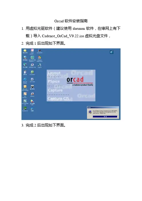
Orcad软件安装指南1.用虚拟光驱软件(建议使用daemon软件,在缘网上有下载)导入Cadence_OrCad_V9.22.iso虚拟光盘文件,2.完成1后出现如下界面。
3.完成2后出现如下界面。
5.出现下列界面,开始安装软件。
6.点击Next,进入下一界面。
7.点击Yes,出现下一界面。
8.点击Next,出现下一界面。
9.点击Next,出现下一界面。
在本界面中输入B,F,I,K(大小写都可以),要换行输入。
10.点击Next,出现如下界面。
输入序列号1356-04-4068。
11.点击Next,出现下列界面。
Name中的字符有可能与上图不一致,别管他。
输入Company (任意字符),12.点击Next,出现下列对话框,可能与下图不一致,别管他。
13.点击Yes,出现下列对话框。
注意:此对话框出现后一定要选中Custom,不能选Typical。
用Browse按钮改变安装路径。
然后点击Next。
出现14.点击Next。
出现下列对话框。
注意:一定要选中Schematics。
如下图所示。
然后点击Next。
一路点击Next,进行安装。
15.当出现下列对话框时,点击“是”。
16.当出现下列对话框时,点击“是”。
17.当出现下列对话框时,如果你的计算机上已安装了Acrobat Reader软件就点击对话框右上角的X,如果没安装就点击确定。
18.下一步出现下列安装完成对话框。
点击Finish按钮,到此步软件安装完成下面需要对本软件进行破解。
破解方法如下步骤:19.用资源管理器,浏览虚拟光盘文件,如下图所示。
20.进入到Crack文件夹。
将PDXOrCAD.exe文件复制到你所安装ORCAD软件的文件夹中。
如下图所示(有可能你的与我不同,主要取决于你的第13步)。
21.双击PDXOrCAD.exe文件,出现下列对话框。
22.点击[…]按钮,出现下列对话框。
23.点击Select按钮,出现下列对话框。
24.点击Apply按钮。


OrCAD PSpice 培训教材培训目标:熟悉PSpice的仿真功能,熟练掌握各种仿真参数的设置方法,综合观测并分析仿真结果,熟练输出分析结果,能够综合运用各种仿真对电路进行分析,学会修改模型参数。
一、PSpice分析过程二、绘制原理图原理图的具体绘制方法差不多在Capture中讲过了,下面要紧讲一下在使用PSpice时绘制原理图应该注意的地点。
1、新建Project时应选择Analog or Mixed-signal Circuit2、调用的器件必须有PSpice模型首先,调用OrCAD软件本身提供的模型库,这些库文件存储的路径为Capture\Library\pspice,此路径中的所有器件都有提供PSpice模型,能够直接调用。
其次,若使用自己的器件,必须保证*.olb、*.lib两个文件同时存在,而且器件属性中必须包含PSpice Template属性。
3、原理图中至少必须有一条网络名称为0,即接地。
4、必须有激励源。
原理图中的端口符号并不具有电源特性,所有的激励源都存储在Source和SourceTM库中。
5、电源两端不同意短路,不同意仅由电源和电感组成回路,也不同意仅由电源和电容组成的割集。
解决方法:电容并联一个大电阻,电感串联一个小电阻。
6、最好不要使用负值电阻、电容和电感,因为他们容易引起不收敛。
三、仿真参数设置1、PSpice能够仿确实类型在OrCAD PSpice中,能够分析的类型有以下8种,每一种分析类型的定义如下:直流分析:当电路中某一参数(称为自变量)在一定范围内变化时,对自变量的每一个取值,计算电路的直流偏置特性(称为输出变量)。
交流分析:作用是计算电路的交流小信号频率响应特性。
噪声分析:计算电路中各个器件对选定的输出点产生的噪声等效到选定的输入源(独立的电压或电流源)上。
即计算输入源上的等效输入噪声。
瞬态分析:在给定输入激励信号作用下,计算电路输出端的瞬态响应。
差不多工作点分析:计算电路的直流偏置状态。

University of PennsylvaniaDepartment of Electrical and Systems EngineeringPSPICEA brief primerContents1.Introductione of PSpice with OrCAD Capture2.1 Step 1: Creating the circuit in Capture2.2 Step 2: Specifying the type of analysis and simulationBIAS or DC analysisDC Sweep simulation2.3 Step 3: Displaying the simulation Results2.4 Other types of Analysis:2.4.1 Transient Analysis2.4.2 AC Sweep Analysis3. Additional Circuit Examples with PSpice3.1 Transformer circuit3.2 AC Sweep of Filter with Ideal Op-amp (Filter circuit)3.3 AC Sweep of Filter with Real Op-amp (Filter Circuit)3.4 Rectifier Circuit (peak detector) and the use of a parametric sweep.Peak Detector simulationParametric Sweep3.5AM Modulated Signal3.6 Center Tap Transformer4.Adding and Creating Libraries: Model and Part Symbol files4.1Using and Adding Vendor Libraries4.2Creating PSpice Symbols from an existing PSpice Model file4.3Creating your own PSpice Model file and Symbol PartsReferences1.INTRODUCTIONSPICE is a powerful general purpose analog and mixed-mode circuit simulator that is used to verify circuit designs and to predict the circuit behavior. This is of particular importance for integrated circuits. It was for this reason that SPICE was originally developed at the Electronics Research Laboratory of the University of California, Berkeley (1975), as its name implies:S imulation P rogram for I ntegrated C ircuits E mphasis.PSpice is a PC version of SPICE (which is currently available from OrCAD Corp. of Cadence Design Systems, Inc.). A student version (with limited capabilities) comes with various textbooks. The OrCAD student edition is called PSpice AD Lite. Information about Pspice AD is available from the OrCAD website: /pspicead.aspxThe PSpice Light version has the following limitations: circuits have a maximum of 64 nodes, 10 transistors and 2 operational amplifiers.SPICE can do several types of circuit analyses. Here are the most important ones: •Non-linear DC analysis: calculates the DC transfer curve.•Non-linear transient and Fourier analysis: calculates the voltage and current as a function of time when a large signal is applied; Fourier analysis gives the frequency spectrum.•Linear AC Analysis: calculates the output as a function of frequency. A bode plot is generated.•Noise analysis•Parametric analysis•Monte Carlo AnalysisIn addition, PSpice has analog and digital libraries of standard components (such as NAND, NOR, flip-flops, MUXes, FPGA, PLDs and many more digital components, ). This makes it a useful tool for a wide range of analog and digital applications.All analyses can be done at different temperatures. The default temperature is 300K.The circuit can contain the following components:•Independent and dependent voltage and current sources•Resistors•Capacitors•Inductors•Mutual inductors•Transmission lines•Operational amplifiers•Switches•Diodes•Bipolar transistors•MOS transistors•JFET•MESFET•Digital gates•and other components (see users manual).2. PSpice with OrCAD Capture (release 9.2 Lite edition)Before one can simulate a circuit one needs to specify the circuit configuration. This can be done in a variety of ways. One way is to enter the circuit description as a text file in terms of the elements, connections, the models of the elements and the type of analysis. This file is called the SPICE input file or source file and has been described somewhere else (see /%7Ejan/spice/spice.overview.html).An alternative way is to use a schematic entry program such as OrCAD CAPTURE. OrCAD Capture is bundled with PSpice Lite AD on the same CD that is supplied with the textbook. Capture is a user-friendly program that allows you to capture the schematic of the circuits and to specify the type of simulation. Capture is non only intended to generate the input for PSpice but also for PCD layout design programs.The following figure summarizes the different steps involved in simulating a circuit with Capture and PSpice. We'll describe each of these briefly through a couple of examples.Figure 1: Steps involved in simulating a circuit with PSpice.The values of elements can be specified using scaling factors (upper or lower case):T or Tera (= 1E12);G or Giga (= E9); MEG or Mega (= E6); K or Kilo (= E3);M or Milli (= E-3); U or Micro (= E-6); N or Nano (= E-9); P or Pico (= E-12) F of Femto (= E-15)Both upper and lower case letters are allowed in PSpice and HSpice. As an example, one can specify a capacitor of 225 picofarad in the following ways:225P, 225p, 225pF; 225pFarad; 225E-12; 0.225NNotice that Mega is written as MEG, e.g. a 15 megaOhm resistor can be specified as15MEG, 15MEGohm, 15meg, or 15E6. Be careful not to use M for Mega! When you write 15Mohm or 15M, Spice will read this as 15 milliOhm!We'll illustrate the different types of simulations for the following circuit:Figure 2: Circuit to be simulated (screen shot from OrCAD Capture).2.1 Step 1: Creating the circuit in Capture2.1.1 Create new project:1.Open OrCAD Capture2.Create a new Project: FILE MENU/NEW_PROJECT3.Enter the name of the project4.Select Analog or Mixed-AD5.When the Create PSpice Project box opens, select "Create Blank Project".A new page will open in the Project Design Manager as shown below.Figure 3: Design manager with schematic window and toolbars (OrCAD screen capture)2.1.2. Place the components and connect the parts1.Click on the Schematic window in Capture.2.To Place a part go to PLACE/PART menu or click on the Place Part Icon. This will opena dialog box shown below.Figure 4: Place Part window3.Select the library that contains the required components. Type the beginning of the namein the Part box. The part list will scroll to the components whose name contains the same letters. If the library is not available, you need to add the library, by clicking on the Add Library button. This will bring up the Add Library window. Select the desired library.For Spice you should select the libraries from the Capture/Library/PSpice folder.Analog: contains the passive components (R,L,C), mutual inductane, transmission line, and voltage and current dependent sources (voltage dependent voltage source E, current-dependent current source F, voltage-dependent current source G and current-dependentvoltage source H).Source: give the different type of independent voltage and current sources, such as Vdc, Idc, Vac, Iac, Vsin, Vexp, pulse, piecewise linear, etc. Browse the library to see what isavailable.Eval: provides diodes (D…), bipolar transistors (Q…), MOS transistors, JFETs (J…),real opamp such as the u741, switches (SW_tClose, SW_tOpen), various digital gates and components.Abm: contains a selection of interesting mathematical operators that can be applied tosignals, such as multiplication (MULT), summation (SUM), Square Root (SWRT),Laplace (LAPLACE), arctan (ARCTAN), and many more.Special:contains a variety of other components, such as PARAM, NODESET, etc.4.Place the resistors, capacitor (from the Analog library), and the DC voltage and currentsource. You can place the part by the left mouse click. You can rotate the components by clicking on the R key. To place another instance of the same part, click the left mousebutton again. Hit the ESC key when done with a particular element. You can add initialconditions to the capacitor. Double-click on the part; this will open the Property window that looks like a spreadsheet. Under the column, labeled IC, enter the value of the initial condition, e.g. 2V. For our example we assume that IC was 0V (this is the default value).5.After placing all part, you need to place the Ground terminal by clicking on the GNDicon (on the right side toolbar – see Fig. 3). When the Place Ground window opens, select GND/CAPSYM and give it the name 0 (i.e. zero). Do not forget to change the name to 0, otherwise PSpice will give an error or "Floating Node". The reason is that SPICEneeds a ground terminal as the reference node that has the node number or name 0 (zero).Figure 5: Place the ground terminal box; the ground terminal should have the name 06.Now connect the elements using the Place Wire command from the menu(PLACE/WIRE) or by clicking on the Place Wire icon.7.You can assign names to nets or nodes using the Place Net Alias command (PLACE/NETALIAS menu). We will do this for the output node and input node. Name these Out andIn, as shown in Figure 2.2.1.3. Assign Values and Names to the parts1.Change the values of the resistors by double-clicking on the number next to the resistor.You can also change the name of the resistor. Do the same for the capacitor and voltage and current source.2.If you haven't done so yet, you can assign names to nodes (e.g. Out and In nodes).3.Save the project2.1.4. NetlistThe netlist gives the list of all elements using the simple format:R_name node1 node2 valueC_name nodex nodey value, etc.1.You can generate the netlist by going to the PSPICE/CREATE NETLIST menu.2.Look at the netlist by double clicking on the Output/ file in the Project ManagerWindow (in the left side File window).Note on Current Directions in elements:The positive current direction in an element such as a resistor is from node 1 to node 2. Node1 is either the left pin or the top pin for an horizontal or vertical positioned element (.e.g aresistor). By rotating the element 180 degrees one can switch the pin numbers. To verify the node numbers you can look at the netlist:e.g. R_R2 node1 node2 10ke.g. R_R2 0 OUT 10kSince we are interested in the current direction from the OUT node to the ground, we need to rotate the resistor R2 twice so that the node numbers are interchanged:R_R2 OUT 0 10k2.2 Step 2: Specifying the type of analysis and simulationAs mentioned in the introduction, Spice allows you do to a DC bias, DC Sweep, Transientwith Fourier analysis, AC analysis, Montecarlo/worst case sweep, Parameter sweep and Temperature sweep. We will first explain how to do the Bias and DC Sweep on the circuit of Figure 2.2.2.1 BIAS or DC analysis1.With the schematic open, go to the PSPICE menu and choose NEW SIMULATIONPROFILE.2.In the Name text box, type a descriptive name, e.g. Bias3.From the Inherit From List: select none and click Create.4.When the Simulation Setting window opens, for the Analyis Type, choose Bias Pointand click OK.5.Now you are ready to run the simulation: PSPICE/RUN6. A window will open, letting you know if the simulation was successful. If there areerrors, consult the Simulation Output file.7.To see the result of the DC bias point simulation, you can open the Simulation Outputfile or go back to the schematic and click on the V icon (Enable Bias VoltageDisplay) and I icon (current display) to show the voltage and currents (see Figure 6).The check the direction of the current, you need to look at the netlist: the current ispositive flowing from node1 to node1 (see note on Current Direction above).Figure 6: Results of the Bias simulation displayed on the schematic.2.2.2 DC Sweep simulationWe will be using the same circuit but will evaluate the effect of sweeping the voltage source between 0 and 20V. We'll keep the current source constant at 1mA.1.Create a new New Simulation Profile (from the PSpice Menu); We'll call it DC Sweep2.For analysis select DC Sweep; enter the name of the voltage source to be swept: V1. Thestart and end values and the step need to be specified: 0, 20 and 0.1V, respectively (see Fig. below).Figure 7: Setting for the DC Sweep simulation.3.Run the simulation. PSpice will generate an output file that contains the values of allvoltages and currents in the circuit.2.3 Step 3: Displaying the simulation ResultsPSpice has a user-friendly interface to show the results of the simulations. Once the simulation is finished a Probe window will open.Figure 8: Probe window1.From the TRACE menu select ADD TRACE and select the voltages and current you liketo display. In our case we'll add V(out) and V(in). Click OK.Figure 9: Add Traces window2.You can also add traces using the "Voltage Markers" in the schematic. From the PSPICEmenu select MARKERS/VOLTAGE LEVELS. Place the makers on the Out and In node.When done, right click and select End Mode.Figure 10: Using Voltage Markers to show the simulation result of V(out) and V(in)3.Go to back to PSpice. You will notice that the waveforms will appear.4.You can add a second Y Axis and use this to display e.g. the current in Resistor R2, asshown below. Go to PLOT/Add Y Axis. Next, add the trace for I(R2).5.You can also use the cursors on the graphs for Vout and Vin to display the actual valuesat certain points. Go to TRACE/CURSORS/DISPLAY6.The cursors will be associated with the first trace, as indicated by the small smallrectangle around the legend for V(out) at the bottom of the window. Left click on the first trace. The value of the x and y axes are displayed in the Probe window. When you right click on V(out) the value of the second cursor will be given together with the difference between the first and second cursor.7.To place the second cursor on the second trace (for V(in)), right click the legend forV(in). You'll notice the outline around V(in) at the bottom of the window. When you right click the second trace the cursor will snap to it. The values of the first and second cursor will be shown in Probe window.8.You can chance the X and Y axes by double clicking on them.9.When adding traces you can perform mathematical calculations on the traces, asindicated in the Add Trace Window to the right of Figure 9.Figure 11: Result of the DC sweep, showing Vout, Vin and the current throughresistor R2. Cursors were used for V(out) and V(in).2.4 Other types of Analysis2.4.1 Transient AnalysisWe'll be using the same circuit as for the DC sweep, except that we'll apply the voltage and current sources by closing a switch, as shown in Figure 12.Figure 12: Circuit used for the transient simulation.1.Insert the SW_TCLOSE switch from the EVAL Library as shown above. Double click onthe switch TCLOSE value and enter the value when the switch closes. Lets makeTCLOSE = 5 ms.2.Set up the Transient Analysis: go to the PSPICE/NEW SIMULATION PROFILE.3.Give it a name (e.g. Transient). When the Simulation Settings window opens, select"Time Domain (Transient)" Analysis. Enter also the Run Time. Lets make it 50 ms. For the Max Step size, you can leave it blank or enter 10us.4.Run PSpice.5. A Probe window in PSpice will open. You can now add the traces to display the results.In the figure below we plotted the current through the capacitor in the top window andthe voltage over the capacitor on the bottom one. We use the cursor to find the timeconstant of the exponential waveform (by finding the 0.632 x V(out)max = 9.48. Thecursor gave a corresponding time of 30ms which gives a time constant of 30-5=25ms (5 ms is subtracted because the switch closed at 5ms).Figure 13: Results of the transient simulation of Figure 12.6.Instead of using a switch we can also use a voltage source that changes over time. Thiswas done in Figure 14 where we used the VPULSE and IPULSE sources from theSOURCE Library. We entered the voltage levels (V1 and V2), the delay (TD), Rise and Fall Times, Pulse Width (PW) and the Period (PER). The values are indicated in the figure below. For details on these parameters click here. A description of other Spice elements can be found in the User’s guide or in the Spice Tutorial.(/~jan/spice/)Figure 14: Circuit with a PULSE voltage and current source.7.After doing the transient simulation results can be displayed as was done before8.The last example of a transient analysis is with a sinusoidal signal VSIN. The circuit isshown below. We made the amplitude 10V and frequency 10 Hz.Figure 15: Circuit with a sinusoidal input.9.Create a Simulation Profiler for the transient analysis and run PSpice.10.The result of the simulation for Vout and Vin are given in the figure below.Figure 16: Transient simulation with a sinusoidal input.2.4.2 AC Sweep AnalysisThe AC analysis will apply a sinusoidal voltage whose frequency is swept over a specified range. The simulation calculates the corresponding voltage and current amplitude and phases for each frequency. When the input amplitude is set to 1V, then the output voltage is basically the transfer function. In contrast to a sinusoidal transient analysis, the AC analysis is not a time domain simulation but rather a simulation of the sinusoidal steady state of the circuit. When the circuit contains non-linear element such as diodes and transistors, the elements will be replaced their small-signal models with the parameter values calculated according to the corresponding biasing point.In the first example, we'll show a simple RC filter corresponding to the circuit of Figure 17.Figure 17: Circuit for the AC sweep simulation.1.Create a new project and build the circuit2.For the voltage source use VAC from the Sources library.3.Make the amplitude of the input source 1V.4.Create a Simulation Profile. In the Simulation Settings window, select AC Sweep/Noise.5.Enter the start and end frequencies and the number of points per decade. For our examplewe use 0.1Hz, 10 kHz and 11, respectively.6.Run the simulation7.In the Probe window, add the traces for the input voltage. We added a second window todisplay the phase in addition to the magnitude of the output voltage. The voltage can be displayed in dB by specifying Vdb(out) in the Add Trace window (type Vdb(out) in the Trace Expression box. For the phase, type VP(out).8.An alternative to show the voltage in dB and phase is to use markers on the schematics:PSPICE/MARKERS/ADVANCED/dBMagnitude or Phase of Voltage, or current. Place the markers on the node of interest.9.We used the cursors in Figure 18 to find the 3dB point. The value is 6.49 Hzcorresponding to a time constant of 25 ms (R1||R2.C). At 10 Hz the attenuation of Vout is11.4db or a factor of 3.72. This corresponds to the value of the amplitude of the outputvoltage obtained during the transient analysis of Figure 16 above.3. Additional Circuit Examples with PSpice3.1 Transformer circuitSPICE has no model for an ideal transformer. An ideal transformer is simulated using mutual inductances such that the transformer ratio N1/N2 = sqrt(L1/L2). The part in PSpice is called TFRM_LINEAR (in the Analog Library). Make the coupling factor K close to or equal to one (ex. K=1) and choose L such that wL >> the resistance seen be the inductor. Thesecondary circuit needs a DC connection to ground. This can be accomplished by adding a large resistor to ground or giving the primary and secondary circuits a common node. The following example illustrates how to simulate a transformer.Figure 3.1.1: Circuit with ideal transformerFor the above example, lets make wL2 >> 500 Ohm or L2> 500/(60*2pi) ; lets make L2 at least 10 times larger, ex. L2=20H. L1 can than be found from the turn ratio: L1/L2 =(N1/N2)^2. For a turn ratio of 10 this makes L1=L2x100=2000H. The circuit as entered in PSpice Capture is shown in Figure 3.1.2 and the result in Figure 3.1.3Figure 3.1.2: Circuit with ideal transformer as entered in PSpice Capture (the transformer TX is modeled by the part XFRM_LINEAR of the Analog Library).Figure 3.1.3: Results of the transient simulation of the above circuit.3.2 AC Sweep of Filter with Ideal Op-amp (Filter circuit)The following circuit will be simulated with PSpice.Figure 3.2.1: Active Filter Circuit with ideal op-amp.We have used off-page connectors (OFFPAGELEFT-R from the CAPSYM library; or by clicking on the off-page icon) for the input and outputs. The name of the connectors can be changed by double-clicking on the name of the off-page connector. By giving the same name to two connectors (or nodes), the two nodes will be connected (no wires are needed). For te voltage source we used the VAC from the SOURCE Library. We gave it an amplitude of 1V so that the output voltage will correspond to the amplification (or transfer function) of the filter. In the Simulation Analysis, select AC Sweep, and enter the starting, ending frequency and the number of points per decade.The result is given in the figure below. The magnitude is given on the left Y axis while the phase is given by the right Y axis. The cursors have been used to find the 3db points of the bandpass filters, corresponding to 0.63 Hz and 32 Hz for the low and high breakpoints,respectively. These numbers correspond to the values of the time constants given in Fig.3.2.1. The phase at these points is -135 and -224 degrees.Figure 3.2.2: Results of the AC sweep of the Active Filter Circuit of the figure above.3.3 AC Sweep of Filter with Real Op-amp (Filter circuit)The circuit with a real op-amp is shown below. We selected the U741 op-amp to build the filter. The simulation results are shown in Figure 3.3.2. As one would expect the differences between the filter with the real and ideal op-amps are minimal in this frequency range.Figure 3.3.1: Active Filter Circuit with the U741 Op-amp.Figure 3.3.2: Results of the AC sweep of the Active Filter Circuit with real Op-amp (U741) of the figure above.3.4 Rectifier Circuit (peak detector) and the use of a parametric sweep.3.4.1: Peak Detector simulationFigure 3.4.1: Rectifier circuit with the D1N4148 diode and a load resistor of 500 Ohm.The results of the simulation are given in Fig. 3.4.2. The ripple has a peak-to-peak value of 777mV as indicated by the cursors. The maximum output voltage is 13.997V which is one volt below the input of 15V.Figure 3.4.2: Simulation results of the rectifier circuit.3.4.2 Parametric SweepIt is interesting to see the effect of the load resistance on the output voltage and its ripple voltage. This can be done using the PARAM part.Figure 3.4.3: Circuit used for the parametric sweep of the load resistor.a. Adding the Parameter Parta.Double click on the value (500 Ohms) of the load resistor R1 to {Rval}. Use curlybrackets. PSpice interprets the text between curly brackets as an expression that itevaluate to a numerical expression. Click OK when done.b.Add the PARAM part to the circuit. You'll find this part in the SPECIAL library.c.Double click on the PARAM part. This will open a spreadsheet like windowshowing the PARAM definition. You will need to add a new column to thisspread sheet. Click on NEW COLUMN and enter for Property Name, Rlval(without the curly brackets).d.You will notice that the new column Rlval has been created. Below the Rlvalenter the initial value for the resistor: lets make it 500, as shown in Figure 3.4.4below.Figure 3.4.4: Property Editor window for the PARAM part, showing the newly created Rlval column.e.While the cell in which you entered the value 500 still selected click theDISPLAY button. You can now specify what to display: select Name and Value.Click OK.f.Click the APPLY button before closing the Property editor.g.Save the design.b. Create the Simulation Profile for the Parametric Analysisa.Select PSPICE/NEW_SIMULATION_PROFILEb.Type in the name of the profile, e.g. Parametricc.In the Simulation Setting window, select Analysis Tab if the window does notopen.d.For the Analysis type select Transient (or the type of analysis you intend toperform; in this example we'll do a transient analysis)e.Under Option, slect Parametric sweep as shown in Figure 3.4.5.f.For the Sweep Variable, select Global Parameter and enter the Parameter name:Rlval. Under sweep type give the start, end and increment for the parameter. We'llused 250, 1kOhm and 250, respectively (see Figure 3.4.5).g.Click OKFigure 3.4.5: Window for the Simulation Settings of the Parametric Sweep.c. Run Spice and Display the waveforms.a.Run PSpiceb.When the simulation is finished the Probe window will open and display a pop upbox with the Available Selection. Select ALL and OK.c.The multiple traces will show, as given in Figure 3.4.6.d.You can use the cursors to determined specific valueson the traces; you can alsoadjust the axis by double-clicking on the Y and X axes.Figure 3.4.6: Results of the parametric sweep of the load resistor, varying from 250 to 1000 Ohm in steps of 250 Ohm.3.5 AM Modulated Signal (AM Modulation)An Amplitude modulated (AM) signal has the expression,v am(t) = [(A + V m cos(2πf m t)] cos(2πf c t) = A[1 + m cos(2πf m t)] cos(2πf c t)in which a sinusoidal high frequency carrier waveform cos(2πf c t) is modulated by asinusoidal modulating of frequency f m. The modulating frequency can be any signal. For this example we’ll assume it is a sinusoid. The modulation index is called m.To generate a AM signal in PSpice we can make use of the Multiplication function MULT that can be found in the ABM library. Figure 3.51 shows the schematic that generates the AM signal over the resistor R1.Figure 3.5.1: Schematic for the generation of an AM signalThe result of a transient simulation is shown in the figure below. One can also look at the Fourier of the simulated output signal. In the Probe window click on the FFT icon, located on the top toolbar, or go to the PSPICE/FOURIER menu. The Fourier spectrum of the displayed trace will be shown. You can change the X axis by double-clicking on it. Figure 3.5.3 gives the Fourier spectrum with the main peak corresponding to the carrier frequency of 5kHz and two side peaks at 4.5 and 5.5 kHz, indicating that the modulating frequency is 500Hz. You can use the cursors to get accurate readings.Figure 3.5.2: Simulated waveform (transient analysis) of the circuit above, with (A=1V,f m=500 Hz, f c=5kHz and m=0.5)Figure 3.5.3: Fourier spectrum of the waveform of Figure 3.5.2.3.6. Center Tap TransformerThere is no direct model in PSpice for a center tap transformer. However, one can usemutually coupled inductors to simulate a center tap transformer. Figure 3.6.1 shows the schematic of the circuit. We used one primary inductor L1 and two secondary inductors L1 and L2 put in series. In addition we added a K-Linear element.Figure 3.6.1: Circuit with Center Tap Transformer with a ratio of 10:1.After placing the element on the schematic give each element its value. Use for the input voltage a sinusoid with amplitude of 100 V and frequency 60 Hz. Notice that we added a small resistor R1 in series with the voltage source and the inductor. This was needed to prevent a short circuit in DC (Spice would give en error without this resistor). We have kept it small equal to 1 Ohm. Assume that we want to have a step-down transformer with a ratio of 10:1 to each secondary output. The ratios of the inductors L2/L1 and L3/L1 must then be equal to 1/102 (or =sqrt(L2/L1)=0.1). We made L1=1000 and L2-L3=10H.Double-click on the K-Linear element and type under the column headings for L1, L2, L3, the values LP, Ls1, Ls2. When done, click the APPLY button and close the propertieswindow.Go to PSpice/CREATE_NETLIST to generate the netlist. To see the list, go to the Project Manager and double-click on OUTPUTs: file. The netlist looks as follows: * source CENTERTAPTRANSFOR2Kn_K1 L_Lp L_Ls1 L_Ls2 1L_Lp 0 N00241 1000L_Ls1 0 VO1 10L_Ls2 VO2 0 10V_V1 N00203 0+SIN 0V 100V 60 0 0 0R_R1 N00203 N00241 1kR_R2 0 VO1 1kR_R3 VO2 0 1kCreate a new Simulation Profile (Transient) with " Time to run = 50ms". The result is shown in Figure 3.6.2. Notice that the max output is 10V as one would expect from a transformer ratio of 10:1 with an input voltage of 100Vmax.. The two outputs are 180 degrees out of phase.。


OrCADPSpice培训教材培训教材培训目标:熟悉PSpice的仿真功能,闇练操纵各类仿真参数的设置方法,综合不雅测并分析仿真成果,闇练输出分析成果,能够或许综合应用各类仿真对电路进行分析,学会修改模型参数。
一、PSpice分析过程二、绘制道理图道理图的具体绘制方法差不多在Capture中讲过了,下面重要讲一下在应用PSpice时绘制道理图应当留意的处所。
1、新建Project时应选择Analog or Mixed-signal Circuit2、调用的器件必须有PSpice模型起首,调用OrCAD软件本身供给的模型库,这些库文件储备的路径为Capture\Library\pspice,此路径中的所有器件都有供给PSpice 模型,能够直截了当调用。
其次,若应用本身的器件,必须包管*.olb、*.lib两个文件同时存在,同时器件属性中必须包含PSpice Template属性。
3、道理图中至少必须有一条收集名称为0,即接地。
4、必须有鼓舞源。
道理图中的端口符号并不具有电源特点,所有的鼓舞源都储备在Source和SourceTM库中。
5、电源两端不许可短路,不许可仅由电源和电感构成回路,也不许可仅由电源和电容构成的割集。
解决方法:电容并联一个大年夜电阻,电感串联一个小电阻。
6、最好不要应用负值电阻、电容和电感,因为他们轻易引起不收敛。
三、仿真参数设置1、PSpice能够或许仿确实类型在OrCAD PSpice中,能够分析的类型有以下8种,每一种分析类型的定义如下:直流分析:当电路中某一参数(称为自变量)在必定范畴内变更时,对自变量的每一个取值,运算电路的直流偏置特点(称为输出变量)。
交换分析:感化是运算电路的交换小旌旗灯号频率响应特点。
噪声分析:运算电路中各个器件对选定的输出点产生的噪声等效到选定的输入源(自力的电压或电流源)上。
即运算输入源上的等效输入噪声。
瞬态分析:在给定输入鼓舞旌旗灯号感化下,运算电路输出端的瞬态响应。
PSPICE 简明教程宾西法尼亚大学电气与系统工程系University of PennsylvaniaDepartment of Electrical and Systems Engineering编译:陈拓2009年8月4日原文作者:Jan Van der Spiegel, ©2006 jan_at_Updated March 19, 2006目录1. 介绍2.带OrCAD Capture 的Pspice 用法2.1 第一步:在Capture 中创建电路2.2 第二步:指定分析和仿真类型偏置或直流分析(BIAS or DC analysis)直流扫描仿真(DC Sweep simulation)2.3 第三步:显示仿真结果2.4 其他分析类型:瞬态分析(Transient Analysis)交流扫描分析(AC Sweep Analysis)3. 附加的使用Pspice 电路的例子3.1 变压器电路3.2 使用理想运算放大器的滤波器交流扫描(滤波器电路)3.3 使用实际运算放大器的滤波器交流扫描(滤波器电路)3.4 整流电路(峰值检波器)和参量扫描的使用峰值检波器仿真(Peak Detector simulation)参量扫描(Parametric Sweep)3.5 AM 调制信号3.6 中心抽头变压器4. 添加和创建库:模型和元件符号文件4.1 使用和添加厂商库4.2 从一个已经存在的Pspice 模型文件创建Pspice 符号4.3 创建你自己的Pspice 模型文件和符号元件参考书目1. 介绍SPICE 是一种强大的通用模拟混合模式电路仿真器,可以用于验证电路设计并且预知电路的行为,这对于集成电路特别重要,1975 年SPICE 最初在加州大学伯克利分校被开发时也是基于这个原因,正如同它的名字所暗示的那样:S imulation P rogram for I ntegrated C ircuits E mphasis.PSpice 是一个PC 版的SPICE(Personal-SPICE),可以从属于Cadence 设计系统公司的OrCAD 公司获得。
Pspice教程(基础篇)Pspice教程课程内容:在这个教程中,我们没有提到关于网络表中的Pspice的网络表文件输出,有关内容将会在后面提到!而且我想对大家提个建议:就是我们不要只看波形好不好,而是要学会分析,分析不是分析的波形,而是学会分析数据,找出自己设计中出现的问题!有时候大家可能会看到,其实电路并没有错,只是有时候我们的仿真设置出了问题,需要修改。
有时候是电路的参数设计的不合理,也可能导致一些莫明的错误!我觉得大家做一个分析后自己看看OutFile文件!点一.直流分析直流分析:PSpice可对大信号非线性电子电路进行直流分析。
它是针对电路中各直流偏压值因某一参数(电源、元件参数等等)改变所作的分析,直流分析也是交流分析时确定小信号线性模型参数和瞬态分析确定初始值所需的分析。
模拟计算后,可以利用Probe功能绘出V o- Vi曲线,或任意输出变量相对任一元件参数的传输特性曲线。
首先我们开启Capture / Capture CIS.打开如下图所示的界面( Fig.1)。
( Fig 1)我们来建立一个新的一程,如下方法打开! ( Fig.2)( Fig.2)我们来选取一个新建的工程文件!我们可以看到以下的提示窗口。
(Fig.3)(Fig.3)我们可以给这个工程取个名字,因为我们要做Pspice仿真,所以我们要勾选第一个选项,在标签栏中选中!其它的选项是什么意思呢?Analog or Mixed A/D 数模混合仿真PC Board Wizard 系统级原理图设计Programmable Logic Wizard CPLD或FPGA设计Schematic 原理图设计接下来我们看到了Pspice工程窗口,即我们的原理图窗口属性的选择。
(Fig.4)(Fig.4)我们在Creat based upon an existing project 下可以看到几个画版工程选项!其中包括:新的空的画版,带层次原理图的画版等等。