MT7812B规格书-中文 _Rev1.15
- 格式:pdf
- 大小:529.29 KB
- 文档页数:7

jw7105b 规格书English Answer:The JW7105B is a high-performance, low-power consumption 32-bit RISC-V microprocessor designed for a wide range of embedded applications. It features a 3-stage pipeline architecture, a 32-bit data bus, and a 32-bit address bus. The JW7105B operates at a maximum frequency of 100MHz and has a power consumption of less than 100mW.The JW7105B has a rich set of peripherals, including a UART, a SPI, an I2C, a PWM, and a timer. It also has a 16-bit ADC and a 16-bit DAC. The JW7105B is packaged in a 48-pin QFN package.The JW7105B is a powerful and versatile microprocessor that is ideal for a wide range of embedded applications. It is easy to use and has a low power consumption, making it a great choice for battery-powered devices.中文回答:JW7105B是一款高性能、低功耗的32位RISC-V微处理器,专为广泛的嵌入式应用而设计。
它采用3级流水线架构、32位数据总线和32位地址总线。

LM78M12中⽂资料LM341/LM78MXX Series3-Terminal Positive Voltage RegulatorsGeneral DescriptionThe LM341and LM78MXX series of three-terminal positive voltage regulators employ built-in current limiting,thermal shutdown,and safe-operating area protection which makes them virtually immune to damage from output overloads.With adequate heatsinking,they can deliver in excess of 0.5A output current.Typical applications would include local (on-card)regulators which can eliminate the noise and de-graded performance associated with single-point regulation.Featuresn Output current in excess of 0.5A n No external componentsn Internal thermal overload protection n Internal short circuit current-limitingn Output transistor safe-area compensationnAvailable in TO-220,TO-39,and TO-252D-PAK packagesn Output voltages of 5V,12V,and 15VConnection DiagramsTO-39Metal Can Package (H)DS010484-5Bottom ViewOrder Number LM78M05CH,LM78M12CH or LM78M15CHSee NS Package Number H03ATO-220Power Package (T)DS010484-6Top ViewOrder Number LM341T-5.0,LM341T-12,LM341T-15,LM78M05CT,LM78M12CT or LM78M15CTSee NS Package Number T03BTO-252DS010484-19Top ViewOrder Number LM78M05CDT See NS Package Number TD03BJuly 1999LM341/LM78MXX Series 3-Terminal Positive Voltage Regulators1999National Semiconductor Corporation /doc/96ef4d46852458fb770b5641.htmlAbsolute Maximum Ratings(Note1)If Military/Aerospace specified devices are required, please contact the National Semiconductor Sales Office/ Distributors for availability and specifications.Lead Temperature(Soldering,10seconds)TO-39Package(H)300?C TO-220Package(T)260?C Storage Temperature Range?65?C to+150?C Operating Junction TemperatureRange?40?C to+125?C Power Dissipation(Note2)Internally Limited Input Voltage5V≤V O≤15V35V ESD Susceptibility TBDElectrical CharacteristicsLimits in standard typeface are for T J=25?C,and limits in boldface type apply over the?40?C to+125?C operating temperature range.Limits are guaranteed by production testing or correlation techniques using standard Statistical Quality Control(SQC) methods.LM341-5.0,LM78M05CUnless otherwise specified:V IN=10V,C IN=0.33µF,C O=0.1µFSymbol Parameter Conditions Min Typ Max Units V O Output Voltage I L=500mA 4.8 5.0 5.2V5mA≤I L≤500mA 4.75 5.0 5.25P D≤7.5W,7.5V≤V IN≤20VV R LINE Line Regulation7.2V≤V IN≤25V I L=100mA50mVI L=500mA100V R LOAD Load Regulation5mA≤I L≤500mA100I Q Quiescent Current I L=500mA410.0mA ?I Q Quiescent Current Change5mA≤I L≤500mA0.57.5V≤V IN≤25V,I L=500mA 1.0V n Output Noise Voltage f=10Hz to100kHz40µVElectrical CharacteristicsLimits in standard typeface are for T J=25?C,and limits in boldface type apply over the?40?C to+125?C operating temperature range.Limits are guaranteed by production testing or correlation techniques using standard Statistical Quality Control(SQC) methods.(Continued)LM341-12,LM78M12CUnless otherwise specified:V IN=19V,C IN=0.33µF,C O=0.1µFSymbol Parameter Conditions Min Typ Max UnitsV O Output Voltage I L=500mA11.51212.5V5mA≤I L≤500mA11.41212.6P D≤7.5W,14.8V≤V IN≤27VV R LINE Line Regulation14.5V≤V IN≤30V I L=100mA120mVI L=500mA240V R LOAD Load Regulation5mA≤I L≤500mA240I Q Quiescent Current I L=500mA410.0mAI Q Quiescent Current Change5mA≤I L≤500mA0.514.8V≤V IN≤30V,I L=500mA 1.0V n Output Noise Voltage f=10Hz to100kHz75µVRipple Rejection f=120Hz,I L=500mA69dBV IN Input Voltage Required I L=500mA17.6V to Maintain Line RegulationV O Long Term Stability I L=500mA60mV/khrs Note1:Absolute maximum ratings indicate limits beyond which damage to the component may occur.Electrical specifications do not apply when operating the de-vice outside of its rated operating conditions.Note2:The typical thermal resistance of the three package types is:T(TO-220)package:θ(JA)=60?C/W,θ(JC)=5?C/WH(TO-39)package:θ(JA)=120?C/W,θ(JC)=18?C/WDT(TO-252)package:θ(JA)=92?C/W,θ(JC)=10?C/W3/doc/96ef4d46852458fb770b5641.htmlSchematic DiagramDS010484-1 /doc/96ef4d46852458fb770b5641.html 4 Typical Performance CharacteristicsPeak Output CurrentDS010484-10Ripple RejectionDS010484-11Ripple RejectionDS010484-12Dropout VoltageDS010484-13Output Voltage(Normalizedto1V at T J=25?C)DS010484-14Quiescent CurrentDS010484-15/doc/96ef4d46852458fb770b5641.html 5Typical Performance Characteristics(Continued)Design ConsiderationsThe LM78MXX/LM341XX fixed voltage regulator series has built-in thermal overload protection which prevents the de-vice from being damaged due to excessive junction tem-perature.The regulators also contain internal short-circuit protection which limits the maximum output current,and safe-area pro-tection for the pass transistor which reduces the short-circuit current as the voltage across the pass transistor is in-creased.Although the internal power dissipation is automatically lim-ited,the maximum junction temperature of the device must be kept below +125?C in order to meet data sheet specifica-tions.An adequate heatsink should be provided to assure this limit is not exceeded under worst-case operating condi-tions (maximum input voltage and load current)if reliable performance is to be obtained).1.0Heatsink ConsiderationsWhen an integrated circuit operates with appreciable cur-rent,its junction temperature is elevated.It is important to quantify its thermal limits in order to achieve acceptable per-formance and reliability.This limit is determined by summing the individual parts consisting of a series of temperature rises from the semiconductor junction to the operating envi-ronment.A one-dimension steady-state model of conduction heat transfer is demonstrated in The heat generated at thedevice junction flows through the die to the die attach pad,through the lead frame to the surrounding case material,to the printed circuit board,and eventually to the ambient envi-ronment.Below is a list of variables that may affect the ther-mal resistance and in turn the need for a heatsink.R θJC (Component Variables)R θCA (Application Variables)Leadframe Size &Material Mounting Pad Size,Material,&LocationNo.of Conduction Pins Placement of Mounting Pad Die SizePCB Size &Material Die Attach MaterialTraces Length &WidthMolding Compound Size and MaterialAdjacent Heat Sources Volume of Air Air FlowAmbient Temperature Shape of Mounting PadQuiescent CurrentDS010484-16Output ImpedanceDS010484-17Line Transient Response DS010484-7Load Transient ResponseDS010484-8/doc/96ef4d46852458fb770b5641.html6Design Considerations(Continued)The LM78MXX/LM341XX regulators have internal thermal shutdown to protect the device from over-heating.Under all possible operating conditions,the junction temperature of the LM78MXX/LM341XX must be within the range of 0?C to 125?C.A heatsink may be required depending on the maxi-mum power dissipation and maximum ambient temperature of the application.To determine if a heatsink is needed,the power dissipated by the regulator,P D ,must be calculated:I IN =I L +I GP D =(V IN ?V OUT )I L +V IN I Gshows the voltages and currents which are present in the circuit.The next parameter which must be calculated is the maxi-mum allowable temperature rise,T R (max):θJA =TR (max)/P D If the maximum allowable value for θJA ?C/w is found to be ≥60?C/W for TO-220package or ≥92?C/W for TO-252pack-age,no heatsink is needed since the package alone will dis-sipate enough heat to satisfy these requirements.If the cal-culated value for θJA fall below these limits,a heatsink is required.As a design aid,Table 1shows the value of the θJA of TO-252for different heatsink area.The copper patterns that we used to measure these θJA are shown at the end of the Application Note Section.reflects the same test results as what are in the Table 1shows the maximum allowable power dissipation vs.ambi-ent temperature for theTO-252device.shows the maximum allowable power dissipation vs.copper area (in 2)for the TO-252device.Please see AN1028for power enhancement techniques to be used with TO-252package.TABLE 1.θJA Different Heatsink AreaLayoutCopper AreaThermal Resistance Top Sice (in 2)*Bottom Side (in 2)(θJA ,?C/W)TO-25210.0123010320.06608730.306040.5305450.7605261047700.284800.470900.6631000.857110157120.0660.06689130.1750.17572140.2840.28461150.3920.39255160.50.553*Tab of device attached to topside copperDS010484-23FIGURE 1.Cross-sectional view of Integrated Circuit Mounted on a printed circuit board.Note that the case temperature is measured at the point where the leadscontact with the mounting pad surface DS010484-24FIGURE 2.Power Dissipation Diagram/doc/96ef4d46852458fb770b5641.html 7Design Considerations(Continued)Typical ApplicationDS010484-20FIGURE 3.θJA vs.2oz Copper Area for TO-252DS010484-22FIGURE 4.Maximum Allowable Power Dissipation vs.Ambient Temperature for TO-252DS010484-21FIGURE 5.Maximum Allowable Power Dissipation vs.2oz.Copper Area for TO-252DS010484-9*Required if regulator input is more than 4inches from input filter capacitor (or if no input filter capacitor is used).**Optional for improved transient response./doc/96ef4d46852458fb770b5641.html 8 Physical Dimensions inches(millimeters)unless otherwise notedTO-39Metal Can Package(H)Order Number LM78M05CH,LM78M12CH or LM78M15CHNS Package Number H03A9/doc/96ef4d46852458fb770b5641.htmlPhysical Dimensions inches(millimeters)unless otherwise noted(Continued)TO-220Power Package(T)Order Number LM341T-5.0,LM341T-12,LM341T-15,LM78M05CT,LM78M12CT or LM78M15CT NS Package Number T03B/doc/96ef4d46852458fb770b5641.html 10Physical Dimensionsinches (millimeters)unless otherwise noted (Continued)LIFE SUPPORT POLICYNATIONAL’S PRODUCTS ARE NOT AUTHORIZED FOR USE AS CRITICAL COMPONENTS IN LIFE SUPPORT DEVICES OR SYSTEMS WITHOUT THE EXPRESS WRITTEN APPROVAL OF THE PRESIDENT AND GENERAL COUNSEL OF NATIONAL SEMICONDUCTOR CORPORATION.As used herein:1.Life support devices or systems are devices or systems which,(a)are intended for surgical implant into the body,or (b)support or sustain life,and whose failure to perform when properly used in accordance with instructions for use provided in the labeling,can be reasonably expected to result in a significant injury to the user.2.A critical component is any component of a life support device or system whose failure to perform can be reasonably expected to cause the failure of the life support device or system,or to affect its safety or effectiveness.National Semiconductor Corporation AmericasTel:1-800-272-9959Fax:1-800-737-7018Email:support@/doc/96ef4d46852458fb770b5641.htmlNational Semiconductor EuropeFax:+49(0)180-5308586Email:europe.support@/doc/96ef4d46852458fb770b5641.htmlDeutsch Tel:+49(0)180-5308585English Tel:+49(0)180-5327832Fran?ais Tel:+49(0)180-5329358Italiano Tel:+49(0)180-5341680National Semiconductor Asia Pacific Customer Response Group Tel:65-2544466Fax:65-2504466Email:sea.support@/doc/96ef4d46852458fb770b5641.htmlNational Semiconductor Japan Ltd.Tel:81-3-5639-7560Fax:81-3-5639-7507/doc/96ef4d46852458fb770b5641.htmlTO-252Order Number LM78M05CDT NS Package Number TD03BLM341/LM78MXX Series 3-Terminal Positive Voltage RegulatorsNational does not assume any responsibility for use of any circuitry described,no circuit patent licenses are implied and National reserves the right at any time without notice to change said circuitry andspecifications.。

MTMT00A08-1415034-19-1415043-17-1393163-37-1415043-1 8-1393163-3MTMT00A0..MT7874002-2017, Rev. © 2015 Tyco Electronics Corporation,a TE Connectivity Ltd. company Datasheets and product specification according to IEC 61810-1 and to be used only together with the ‘Definitions’ section.Datasheets and product data is subject to the terms of the disclaimer and all chapters of the ‘Definitions’ section, available at /definitionsDatasheets, product data, ‘Definitions’ sec-tion, application notes and all specifications are subject to change.1SCHRACKn Snap-on mounting on DIN-rail n Screw mountingn Pozidrive screws with rising clamp terminals n Logical layout of input-/output connections n White marking areaMT DIN-rail sockets with screw-type terminalsMT 78 750 MT3 DIN-rail socket with screw-type terminals, 11-pin MT 78 755 MT2 DIN-rail socket with screw-type terminals, 8-pinMT78 760 MT3 DIN-rail socket with screw-type terminals, 11-pinMT 78 740 MT3 DIN-rail socket with screw-type terminals, 11-pin MT 78 745 MT2 DIN-rail socket with screw-type terminals, 8-pinGeneral Purpose Relays AccessoriesAccessories Multimode Relay MTZF0235-BF0103-BS0414-AB S0414-ACF0103-BS0311-BB S0414-AAF0200-BS0366-ASocket system MT 78 740 and MT 78 745n 8/11 pin socket for MT2 / MT3n Double A2 screw for simple further connection of coil supplyZ Zb02-2017, Rev. 0217© 2015 Tyco Electronics Corporation, a TE Connectivity Ltd. company Datasheets and product specificationaccording to IEC 61810-1 and to be usedonly together with the ‘Definitions’ section.Datasheets and product data is subject to theterms of the disclaimer and all chapters ofthe ‘Definitions’ section, available at/definitionsDatasheets, product data, ‘Definitions’ sec-tion, application notes and all specificationsare subject to change.2SCHRACKType Part NumberMT 28 800Metal retaining clip MT 8-1393163-0LED and Protection modules for MT 78 740, MT 78 745Type Part NumberMTM T0 0A0Protection diode 1N4007 (A1+, A2-) 7-1393163-6MTM U0 730RC-network 110...230 VAC 7-1393163-8MTM L0 024red LED 24 VAC / VDC 7-1393163-4Function modules for MT 78 740, MT 78 745Type Part NumberMTM Z0 W00 Delay ON 7-1393163-9MTM F0 W00Multifunction 7-1393163-3Technical data - Function modulesNominal voltage 24...240 VDC / VACMains frequency 48...63 HzPrecision of time setting + 0.5 %Readiness for repetition ≤ 0.5 % or 5 msInfluence of temperature ≤ 0.1 %/°CTime range switchable 0.05s...240h in 8 rangesMaterial compliance: EU RoHS/ELV, China RoHS, REACH, Halogen contentrefer to the Product Compliance Support Center at/customersupport/rohssupportcenterAmbient temperature range -25…+55˚CGeneral Purpose RelaysAccessoriesAccessories Multimode Relay MT (Continued)ApprovalsVDE Cert. No. 40009096, cULus E135149Technical data MT78 750/755/760/740/745Rated voltage/Max. switching voltage AC 240/400 VACRated current 10 ADielectric strengthcoil-contact circuit 2500 V rmsopen contact circuit 1500 V rmsadjacent contact circuit 2500 V rmsClearance / creepage coil-contact circuit ≥ 2.8/4 mmMaterial group of insulation parts IIIaInsulation to IEC 60664-1Type of insulation coil-contact circuit basicopen contact circuit functionaladjacent contact circuits basicRated insulation voltage 250 VPollution degree 2Rated voltage system 230/400 VOvervoltage category IIIMaterial compliance: EU RoHS/ELV, China RoHS, REACH, Halogen contentrefer to the Product Compliance Support Center at/customersupport/rohssupportcenterAmbient temperature range -20…+80˚CTerminals screwTerminal screw torque acc. IEC 61984 0.5 Nmmax. 0.7 NmWire strip length 9 mmWire cross sectionsingle wire 2 x 2.5 mm2fine wire 2 x 2.5 mm2with bootlace crimp (DIN 46228/1) 2 x 1.5 mm2Insertion cycles A (10)Max. Insertion Force total 100 NMounting distance ≥ 0 mm, dense packingWeightMT 78 750/760 54 gMT 78 755 47 gMT 78 740 62 gMT 78 745 56 gPackaging unit 25 pcsDIN-rail sockets with screw-type terminalsType Part NumberMT 78 750DIN-rail socket with screw-type 1415035-1terminals, 11-pinMT 78 755DIN-rail socket with screw-type 3-1415035-1terminals, 8-pinMT 78 760DIN-rail socket with screw-type 8-1415034-1terminals, 11-pinMT 78 740DIN-rail socket with screw-type 8-1393163-3terminals, 11-pinMT 78 745DIN-rail socket with screw-type8-1393163-4F0201-BF0203-BF0204-B02-2017, Rev. 0117© 2015 Tyco Electronics Corporation, a TE Connectivity Ltd. company Datasheets and product specificationaccording to IEC 61810-1 and to be usedonly together with the ‘Definitions’ section.Datasheets and product data is subject to theterms of the disclaimer and all chapters ofthe ‘Definitions’ section, available at/definitionsDatasheets, product data, ‘Definitions’ sec-tion, application notes and all specificationsare subject to change.3SCHRACKFunction modules for MT 78 740, MT 78 745FunctionDelay ONDelay OFFsingle shot leading edgesingle shot trailing edgeDelay ONtriggerd by signal contactsingle shotflasher starting with pauseflasher starting with pulseAccessories Multimode Relay MT(Continued)Technical data MT78 602/603/612/613Rated voltage/Max. switching voltage AC 240/400 VACRated current 10 ADielectric strengthcoil-contact circuit 2500 V rmsopen contact circuit 1500 V rmsadjacent contact circuits 2500 V rmsClearance / creepage coil-contact circuit ≥ 2.8/4 mmMaterial group of insulation parts IIIaInsulation to IEC 60664-1Type of insulation coil-contact circuit basicopen contact circuit functionaladjacent contact circuits basicRated insulation voltage 250 VPollution degree 2Rated voltage system 230/400 VOvervoltage category IIIMaterial compliance: EU RoHS/ELV, China RoHS, REACH, Halogen contentrefer to the Product Compliance Support Center at/customersupport/rohssupportcenterAmbient temperature range -40…+70˚CTerminals pcb, solder terminalsInsertion cycles A (10)Max. Insertion Force total 100 NMounting distance ≥ 0 mm, dense packingResistance to soldering heat 270°C/10sWeight 7 gPackaging unit 25 pcsSockets with solder and PCB terminalsType Part NumberMT 78 612Socket 8-pin with solder terminals 7-1415043-1MT 78 613Socket 11-pin with solder terminals 8-1415043-1MT 78 602Socket 8-pin with PCB terminals 9-1415043-1MT 78 603Socket 11-pin with PCB terminals 1415044-1MT 78 613Socket 11-pin with solder terminalsMT 78 603Socket 11-pin with PCB terminalsF0107-AS0309-AAF0104-AS0309-ABF0105-AS0309-ACF0106-AS0309-ADGeneral Purpose RelaysAccessoriesMTMT00A08-1415034-19-1415043-17-1393163-37-1415043-1 8-1393163-3MTMT00A0..MT78740。
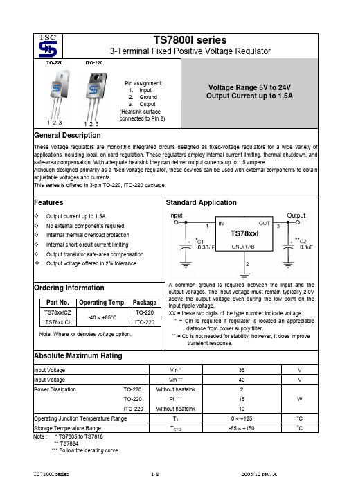
TS7800I series3-Terminal Fixed Positive Voltage RegulatorPin assignment:1. Input2. Ground3. Output (Heatsink surfaceconnected to Pin 2)Voltage Range 5V to 24V Output Current up to 1.5AGeneral DescriptionThese voltage regulators are monolithic integrated circuits designed as fixed-voltage regulators for a wide variety of applications including local, on-card regulation. These regulators employ internal current limiting, thermal shutdown, and safe-area compensation. With adequate heatsink they can deliver output currents up to 1.5 ampere.Although designed primarily as a fixed voltage regulator, these devices can be used with external components to obtain adjustable voltages and currents.This series is offered in 3-pin TO-220, ITO-220 package.FeaturesOutput current up to 1.5A No external components required Internal thermal overload protection Internal short-circuit current limitingOutput transistor safe-area compensationOutput voltage offered in 2% toleranceOrdering InformationNote: Where xx denotes voltage option. Part No. Operating Temp. Package TS78xxICZ TO-220 TS78xxICI -40 ~ +85o CITO-220Standard ApplicationA common ground is required between the input and the output voltages. The input voltage must remain typically 2.0V above the output voltage even during the low point on theInput ripple voltage. XX = these two digits of the type number indicate voltage.* = Cin is required if regulator is located an appreciable distance from power supply filter.** = Co is not needed for stability; however, it does improvetransient response.Absolute Maximum RatingInput Voltage Vin * 35 V Input VoltageVin ** 40 V Power Dissipation TO-220 TO-220 ITO-220 Without heatsinkPt *** Without heatsink2 15 10 WOperating Junction Temperature Range T J 0 ~ +125 o C Storage Temperature Range T STG-65 ~ +150oCNote : * TS7805 to TS7818 ** TS7824ITO-220TS7805I Electrical Characteristics(Vin=10V, Iout=500mA, 0o C ≤Tj ≤125o C, Cin=0.33uF, Cout=0.1uF; unless otherwise specified.)Parameter Symbol Test Conditions Min Typ Max UnitTj=25o C4.90 55.10 Output voltageVout7.5V ≤Vin ≤20V, 10mA ≤Iout ≤1.5A, PD ≤15W4.80 55.20V7.5V ≤Vin ≤25V -- 3 100 Line Regulation REGline Tj=25o C 8V ≤Vin ≤12V -- 1 5010mA ≤Iout ≤1.5A -- 15 100 Load Regulation REGload Tj=25o C250mA ≤Iout ≤750mA-- 5 50mVQuiescent Current Iq Iout=0, Tj=25o C -- 4.2 8 7.5V ≤Vin ≤25V -- -- 1.3Quiescent Current Change ∆Iq10mA ≤Iout ≤1.5A -- -- 0.5mA Output Noise Voltage Vn 10Hz ≤f ≤100KHz, Tj=25o C-- 40 -- uV Ripple Rejection Ratio RR f=120Hz, 8V ≤Vin ≤18V 6278--dBVoltage DropVdrop Iout=1.0A, Tj=25o C -- 2 -- VOutput Resistance Rout f =1KHz-- 17 -- m Ω Output Short Circuit Current Ios Tj=25o C -- 750 -- mAPeak Output CurrentIo peakTj=25o C-- 2.2 -- A Temperature Coefficient of Output Voltage∆Vout/ ∆Tj Iout =10mA, 0o C ≤Tj ≤125o C-- -0.6 -- mV/oCTS7806I Electrical Characteristics(Vin=11V, Iout=500mA, 0o C ≤Tj ≤125o C, Cin=0.33uF, Cout=0.1uF; unless otherwise specified.)Parameter Symbol Test Conditions Min Typ Max UnitTj=25o C5.88 66.12 Output VoltageVout8.5V ≤Vin ≤21V, 10mA ≤Iout ≤1.5A, PD ≤15W5.76 66.24V8.5V ≤Vin ≤25V -- 5 120 Line Regulation REGline Tj=25o C 9V ≤Vin ≤13V -- 1.5 6010mA ≤Iout ≤1.5A -- 14 120 Load Regulation REGload Tj=25o C250mA ≤Iout ≤750mA -- 4 60mVQuiescent Current Iq Iout=0, Tj=25o C -- 4.3 8 8.5V ≤Vin ≤25V -- -- 1.3 Quiescent Current Change ∆Iq 10mA ≤Iout ≤1.5A -- -- 0.5 mA Output Noise Voltage Vn 10Hz ≤f ≤100KHz, Tj=25o C-- 45 -- uVRipple Rejection Ratio RR f=120Hz, 9V ≤Vin ≤19V 59 75 -- dBVoltage DropVdrop Iout=1.0A, Tj=25o C -- 2 -- VOutput Resistance Rout f =1KHz-- 19 -- m Ω Output Short Circuit Current Ios Tj=25o C -- 550 -- mAPeak Output CurrentIo peakTj=25o C-- 2.2 -- ATemperature Coefficient ofOutput Voltage ∆Vout/ ∆Tj Iout 10mA, 0o C ≤Tj ≤125o C-- -0.7 -- mV/oC z Pulse testing techniques are used to maintain the junction temperature as close to the ambient temperature aspossible, and thermal effects must be taken into account separately.TS7808I Electrical Characteristics(Vin=14V, Iout=500mA, 0o C ≤Tj ≤125o C, Cin=0.33uF, Cout=0.1uF; unless otherwise specified.)Parameter Symbol Test Conditions Min Typ Max UnitTj=25o C7.84 8 8.16 Output VoltageVout10.5V ≤Vin ≤23V,10mA ≤Iout ≤1.5A, PD ≤15W7.68 8 8.32V10.5V ≤Vin ≤25V -- 6 160 Line Regulation REGline Tj=25o C 11V ≤Vin ≤17V -- 2 8010mA ≤Iout ≤1.5A -- 12 160 Load Regulation REGload Tj=25o C250mA ≤Iout ≤750mA -- 4 80mVQuiescent Current Iq Iout=0, Tj=25o C -- 4.3 8 10.5V ≤Vin ≤25V -- -- 1Quiescent Current Change ∆Iq 10mA ≤Iout ≤1.5A -- -- 0.5 mA Output Noise Voltage Vn 10Hz ≤f ≤100KHz, Tj=25o C-- 52 -- uVRipple Rejection Ratio RR f=120Hz, 11V ≤Vin ≤21V 56 72 -- dB Voltage DropVdrop Iout=1.0A, Tj=25o C -- 2 -- VOutput Resistance Rout f =1KHz-- 16 -- m Ω Output Short Circuit Current Ios Tj=25o C -- 450 -- mAPeak Output CurrentIo peakTj=25o C-- 2.2 -- A Temperature Coefficient of Output Voltage∆Vout/ ∆Tj Iout =10mA, 0o C ≤Tj ≤125o C-- -0.8 -- mV/oCTS7809I Electrical Characteristics(Vin=15V, Iout=500mA, 0o C ≤Tj ≤125o C, Cin=0.33uF, Cout=0.1uF; unless otherwise specified.)Parameter Symbol Test Conditions Min Typ Max UnitTj=25o C8.82 9 9.18 Output VoltageVout11.5V ≤Vin ≤23V,10mA ≤Iout ≤1.5A, PD ≤15W8.64 9 9.36V11.5V ≤Vin ≤26V -- 6 180 Line Regulation REGline Tj=25o C 12V ≤Vin ≤17V -- 2 9010mA ≤Iout ≤1.5A -- 12 180 Load Regulation REGload Tj=25o C250mA ≤Iout ≤750mA -- 4 90mVQuiescent Current Iq Iout=0, Tj=25o C -- 4.3 8 11.5V ≤Vin ≤26V -- -- 1 Quiescent Current Change ∆Iq 10mA ≤Iout ≤1.5A -- -- 0.5 mA Output Noise Voltage Vn 10Hz ≤f ≤100KHz, Tj=25o C-- 52 -- uVRipple Rejection Ratio RR f=120Hz, 12V ≤Vin ≤22V 55 72 -- dBVoltage DropVdrop Iout=1.0A, Tj=25o C -- 2 -- VOutput Resistance Rout f =1KHz-- 16 -- m Ω Output Short Circuit Current Ios Tj=25o C -- 450 -- mAPeak Output CurrentIo peakTj=25o C-- 2.2 -- ATemperature Coefficient ofOutput Voltage ∆Vout/ ∆Tj Iout 10mA, 0o C ≤Tj ≤125o C -- -1 -- mV/oC z Pulse testing techniques are used to maintain the junction temperature as close to the ambient temperature aspossible, and thermal effects must be taken into account separately.TS7810I Electrical Characteristics(Vin=16V, Iout=500mA, 0o C ≤Tj ≤125o C, Cin=0.33uF, Cout=0.1uF; unless otherwise specified.)Parameter Symbol Test Conditions Min Typ Max UnitTj=25o C 9.8 10 10.2Output VoltageVout12.5V ≤Vin ≤25V,10mA ≤Iout ≤1.5A, PD ≤15W9.6 10 10.4V12.5V ≤Vin ≤28V -- 7 200 Line Regulation REGline Tj=25o C 13V ≤Vin ≤17V -- 2 10010mA ≤Iout ≤1.5A -- 12 200 Load Regulation REGload Tj=25o C250mA ≤Iout ≤750mA -- 4 100mVQuiescent Current Iq Iout=0, Tj=25o C -- 4.3 8 12.5V ≤Vin ≤28V -- -- 1Quiescent Current Change ∆Iq 10mA ≤Iout ≤1.5A -- -- 0.5 mA Output Noise Voltage Vn 10Hz ≤f ≤100KHz, Tj=25o C-- 70 -- uVRipple Rejection Ratio RR f=120Hz, 13V ≤Vin ≤23V 55 71 -- dB Voltage DropVdrop Iout=1.0A, Tj=25o C -- 2 -- VOutput Resistance Rout f =1KHz-- 18 -- m Ω Output Short Circuit Current Ios Tj=25o C -- 400 -- mAPeak Output CurrentIo peakTj=25o C-- 2.2 -- ATemperature Coefficient of Output Voltage∆Vout/ ∆Tj Iout =10mA, 0o C ≤Tj ≤125o C -- -1 -- mV/oCTS7812I Electrical Characteristics(Vin=19V, Iout=500mA, 0o C ≤Tj ≤125o C, Cin=0.33uF, Cout=0.1uF; unless otherwise specified.)Parameter Symbol Test Conditions Min Typ Max UnitTj=25o C11.76 12 12.24 Output VoltageVout14.5V ≤Vin ≤27V,10mA ≤Iout ≤1.5A, PD ≤15W11.52 12 12.48V14.5V ≤Vin ≤30V -- 10 240 Line Regulation REGline Tj=25o C 15V ≤Vin ≤19V -- 3 12010mA ≤Iout ≤1.5A -- 12 240 Load Regulation REGload Tj=25o C250mA ≤Iout ≤750mA -- 4 120mVQuiescent Current Iq Tj=25o C, Iout=0--4.3814.5V ≤Vin ≤30V -- -- 1 Quiescent Current Change ∆Iq 10mA ≤Iout ≤1.5A -- -- 0.5 mA Output Noise Voltage Vn 10Hz ≤f ≤100KHz, Tj=25o C-- 75 -- uVRipple Rejection Ratio RR f=120Hz, 15V ≤Vin ≤25V 55 71 -- dBVoltage DropVdrop Iout=1.0A, Tj=25o C -- 2 -- VOutput Resistance Rout f =1KHz-- 18 -- m Ω Output Short Circuit Current Ios Tj=25o C -- 350 -- mAPeak Output CurrentIo peakTj=25o C-- 2.2 -- ATemperature Coefficient ofOutput Voltage ∆Vout/ ∆Tj Iout 10mA, 0o C ≤Tj ≤125o C -- -1 -- mV/oC z Pulse testing techniques are used to maintain the junction temperature as close to the ambient temperature aspossible, and thermal effects must be taken into account separately.TS7815I Electrical Characteristics(Vin=23V, Iout=500mA, 0o C ≤Tj ≤125o C, Cin=0.33uF, Cout=0.1uF; unless otherwise specified.)Parameter Symbol Test Conditions Min Typ Max UnitTj=25o C14.70 15 15.30 Output VoltageVout17.5V ≤Vin ≤30V,10mA ≤Iout ≤1.5A, PD ≤15W14.40 15 15.60V17.5V ≤Vin ≤30V -- 12 300 Line Regulation REGline Tj=25o C 18V ≤Vin ≤22V -- 3 15010mA ≤Iout ≤1.5A -- 12 300 Load Regulation REGload Tj=25o C250mA ≤Iout ≤750mA -- 4 150mVQuiescent Current Iq Tj=25o C, Iout=0--4.3817.5V ≤Vin ≤30V -- -- 1Quiescent Current Change ∆Iq 10mA ≤Iout ≤1.5A -- -- 0.5 mA Output Noise Voltage Vn 10Hz ≤f ≤100KHz, Tj=25o C-- 90 -- uVRipple Rejection Ratio RR f=120Hz, 18V ≤Vin ≤28V 54 70 -- dB Voltage DropVdrop Iout=1.0A, Tj=25o C -- 2 -- VOutput Resistance Rout f =1KHz-- 19 -- m Ω Output Short Circuit Current Ios Tj=25o C -- 230 -- mAPeak Output CurrentIo peakTj=25o C-- 2.2 -- ATemperature Coefficient of Output Voltage∆Vout/ ∆Tj Iout =10mA, 0o C ≤Tj ≤125o C -- -1 -- mV/oCTS7818I Electrical Characteristics(Vin=27V, Iout=500mA, 0o C ≤Tj ≤125o C, Cin=0.33uF, Cout=0.1uF; unless otherwise specified.)Parameter Symbol Test Conditions Min Typ Max UnitTj=25o C17.64 18 18.36 Output VoltageVout21V ≤Vin ≤33V, 10mA ≤Iout ≤1.5A, PD ≤15W17.28 18 18.72V21V ≤Vin ≤33V -- 15 360 Line Regulation REGline Tj=25o C 22V ≤Vin ≤26V -- 5 18010mA ≤Iout ≤1.5A -- 12 360 Load Regulation REGload Tj=25o C250mA ≤Iout ≤750mA -- 4 180mVQuiescent Current Iq Tj=25o C, Iout=0--4.5821V ≤Vin ≤33V -- -- 1 Quiescent Current Change ∆Iq 10mA ≤Iout ≤1.5A -- -- 0.5 mA Output Noise Voltage Vn 10Hz ≤f ≤100KHz, Tj=25o C -- 110 -- uV Ripple Rejection Ratio RR f=120Hz, 21V ≤Vin ≤31V 54 70 -- dBVoltage DropVdrop Iout=1.0A, Tj=25o C -- 2 -- VOutput Resistance Rout f =1KHz-- 22 -- m Ω Output Short Circuit Current Ios Tj=25o C -- 200 -- mAPeak Output CurrentIo peakTj=25o C-- 2.2 -- ATemperature Coefficient ofOutput Voltage ∆Vout/ ∆Tj Iout 10mA, 0o C ≤Tj ≤125o C -- -1 -- mV/oC z Pulse testing techniques are used to maintain the junction temperature as close to the ambient temperature aspossible, and thermal effects must be taken into account separately.TS7824I Electrical Characteristics(Vin=33V, Iout=500mA, 0o C ≤Tj ≤125o C, Cin=0.33uF, Cout=0.1uF; unless otherwise specified.)Parameter Symbol Test Conditions Min Typ Max UnitTj=25o C23.52 24 24.48 Output VoltageVout27V ≤Vin ≤38V, 10mA ≤Iout ≤1.5A, PD ≤15W23.04 24 24.96V27V ≤Vin ≤38V -- 18 480 Line Regulation REGline Tj=25o C 28V ≤Vin ≤32V -- 6 24010mA ≤Iout ≤1.5A -- 12 480 Load Regulation REGload Tj=25o C250mA ≤Iout ≤750mA -- 4 240mVQuiescent Current Iq Iout=0, Tj=25o C -- 4.6 8 27V ≤Vin ≤38V -- -- 1Quiescent Current Change ∆Iq 10mA ≤Iout ≤1.5A -- -- 0.5 mA Output Noise Voltage Vn 10Hz ≤f ≤100KHz, Tj=25o C -- 170 -- uVRipple Rejection Ratio RR f=120Hz, 27V ≤Vin ≤37V 54 70 -- dB Voltage DropVdrop Iout=1.0A, Tj=25o C -- 2 -- VOutput Resistance Rout f =1KHz-- 28 -- m Ω Output Short Circuit Current Ios Tj=25o C -- 150 -- mAPeak Output CurrentIo peakTj=25o C-- 2.2 -- ATemperature Coefficient ofOutput Voltage ∆Vout/ ∆Tj Iout =10mA, 0o C ≤Tj ≤125o C-- -1.5 -- mV/oC z Pulse testing techniques are used to maintain the junction temperature as close to the ambient temperature aspossible, and thermal effects must be taken into account separately.z This specification applies only for DC power dissipation permitted by absolute maximum ratings.Electrical Characteristics CurveFIGURE 1 - Worst Case Power Dissipation v.s.Ambient TemperatureFIGURE 2 - Peak Output Current v.s.Input-Output Differential VoltageFIGURE 3 – Quiescent Current v.s.Junction TemperatureFIGURE 4 – Input Output Differential v.s.Junction TemperatureFIGURE 5 – Output Voltage v.s.Junction TemperatureFIGURE 6 – Output Impedance v.s.Output Voltage。

Information their respective owners.Rev. Gfurnished by Analog Devices is believed to be accurate and reliable. However , no responsibility is assumed by Analog Devices for its use, nor for any infringements of patents or other rights of third parties that may result from its use. Speci cations subject to change without notice. No license is granted by implication or otherwise under any patent or patent rights of Analog Devices. T rademarks and registered trademarks are the property ofOne Technology Way, P.O. Box 9106, Norwood, MA 02062-9106, U.S.A.Tel: 781.329.4700 Fax: 781.461.3113 ©2000–2011 Analog Devices, Inc. All rights reserved.引脚配置01525-001OUT A 1V–2+IN 3V+5–IN4AD8601TOP VIEW (Not to Scale)图1. 5引脚SOT-23(RJ 后缀)OUT A 1–IN A 2+IN A 3V–4V+8OUT B 7–IN B6+IN B5AD8602TOP VIEW (Not to Scale)01525-002图2. 8引脚MSOP(RM 后缀)和8引脚SOIC(R 后缀)01525-0031234567AD8604–IN A +IN A V+OUT B –IN B +IN B OUT A 141312111098–IN D +IN D V–OUT C–IN C +IN C OUT D TOP VIEW (Not to Scale)图3. 14引脚TSSOP(RU 后缀)和14引脚SOIC(R 后缀)12345678161514131211109–IN A +IN A V+OUT B–IN B +IN B OUT A –IN D+IN D V–OUT CNCNCNC = NO CONNECT–IN C +IN C OUT D TOP VIEW (Not to Scale)AD860401525-004图4. 16引脚紧缩小型封装QSOP(RQ 后缀)ADI 中文版数据手册是英文版数据手册的译文,敬请谅解翻译中可能存在的语言组织或翻译错误,ADI 不对翻译中存在的差异或由此产生的错误负责。
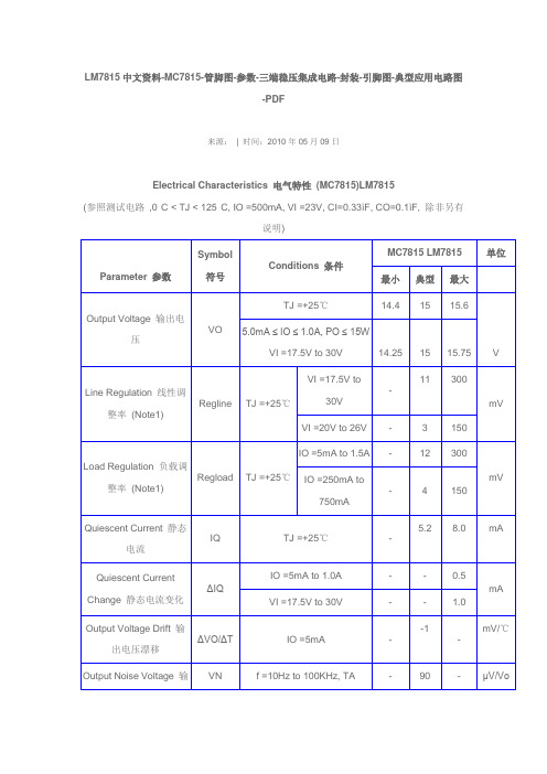
LM7815中文资料目录1.lm7815介绍2.实际应用3.引脚序号、引脚功能4.lm7815应用电路5.7815电参数三端稳压集成电路lm7815。
电子产品中,常见的三端稳压集成电路有正电压输出的lm78 ×× 系列和负电压输出的lm79××系列。
顾名思义,三端IC是指这种稳压用的集成电路,只有三条引脚输出,分别是输入端、接地端和输出端。
它的样子象是普通的三极管,TO- 220 的标准封装,也有lm9013样子的TO-92封装。
1.lm7815介绍用lm78/lm79系列三端稳压IC来组成稳压电源所需的外围元件极少,电路内部还有过流、过热及调整管的保护电路,使用起来可靠、方便,而且价格便宜。
该系列集成稳压IC型号中的lm78或lm79后面的数字代表该三端集成稳压电路的输出电压,如lm7806表示输出电压为正6V,lm7909表示输出电压为负9V。
因为三端固定集成稳压电路的使用方便,电子制作中经常采用。
最大输出电流1.5A,LM78XX系列输出电压分别为5V;6V;8V;9V;10V;12V;15V;18V;24V。
2.实际应用在实际应用中,应在三端集成稳压电路上安装足够大的散热器(当然小功率7815IC内部电路图.的条件下不用)。
当稳压管温度过高时,稳压性能将变差,甚至损坏。
当制作中需要一个能输出1.5A以上电流的稳压电源,通常采用几块三端稳压电路并联起来,使其最大输出电流为N个1.5A,但应用时需注意:并联使用的集成稳压电路应采用同一厂家、同一批号的产品,以保证参数的一致。
另外在输出电流上留有一定的余量,以避免个别集成稳压电路失效时导致其他电路的连锁烧毁。
在lm78 ** 、lm79 ** 系列三端稳压器中最常应用的是TO-220 和TO-202 两种封装。
这两种封装的图形以及引脚序号、引脚功能如附图所示。
图中的引脚号标注方法是按照引脚电位从高到底的顺序标注的。