单节锂离子电池保护芯片
- 格式:pdf
- 大小:262.61 KB
- 文档页数:6

单节锂离子电池保护芯片的设计前言锂离子电池保护芯片的设计与其封装结构密切相关,为封装在锂离子电池内部的保护电路的基本结构。
在正常情况下,充电控制端CO 和放电控制端DO 为高电位,N型放电控制管FET1和充电控制管FET2处于导通状态,电路的工作方式可以是电池向负载放电,也可以是充电器对电池进行充电;当保护电路检测到异常现象(过充电、过放电和过电流)时,使CO 或DO输出低电平,从而切断充电或放电回路,实现保护功能。
为了有效利用放电电流或充电电流,FET1和FET2采用导通电阻很小的功率管。
它们的选择原则除了导通电阻要小,还要求体积小,并且关闭时源漏击穿电压要能经受不匹配充电器的影响。
从理论上说,FET1和FET2可以用N 管也可以用P 管。
但由于单节锂离子电池保护电路的电源电压较低,为了减小导通电阻,一般都采用N管。
图1中二极管是FET1和FET2的寄生二极管,它们的存在使系统在过放电状态下能对电池充电,在过充电状态下能对负载放电。
图1 3.6V 锂离子电池保护电路封装结构锂离子电池保护芯片的应用场合要求其具有低电流驱动、高精度检测的特点,另外由于保护电路的供电电源即为电池电压,因此在电池电压的变化范围内,保护电路必须正常工作,本文根据图1 所示的连接关系,设计一种低功耗单节锂离子电池保护芯片,其电池电压可以在1V—5.5V范围内变化。
系统结构设计锂离子电池保护芯片的基本功能是进行过充电保护、过放电保护和过电流保护,其中过电流保护包括充电过流保护和放电过流保护。
下面以保护电路的基本功能为出发点,分析其系统的组成。
检测异常现象锂离子电池保护电路为了实现其基本功能,首先需要检测异常现象。
过充电和过放电检测是将电池电压进行分压(采样)后与基准电压比较实现的;而对于过流检测,保护芯片首先将充放电过程中的电流转化为在功率管FET1、FET2上的电压,然后通过VM与基准电压比较完成,放电过流检测的是正电压,充电过流检测的是负电压。
DP4056替代LTC4056TP4056锂电池充电保护芯⽚_1000mADP4056是⼀款完整的单节锂离⼦电池采⽤恒定电流/恒定电压线性充电器。
其底部带有散热⽚的SOP8/MSOP封装与较少的外部元件数⽬使得DP4056成为便携式应⽤的理想选择。
DP4056适合USB电源和适配器电源⼯作。
由于采⽤了内部PMOSFET架构,加上防倒充电路,所以不需要外部隔离⼆极管。
热反馈可对充电电流进⾏⾃动调节,以便在⼤功率操作或⾼环境温度条件下对芯⽚温度加以限制。
充电电压固定于4.2V,⽽充电电流可通过⼀个电阻器进⾏外部设置。
当充电电流在达到最终浮充电压之后降⾄设定值1/10时,DP4056将⾃动终⽌充电循环。
当输⼊电压(交流适配器或USB电源)被拿掉时,⾃动进⼊⼀个低电流状态,将电池漏电流降⾄2uA以下。
在有电源时也可置于停机模式,以⽽将供电电流降⾄55uA。
的其他特点包括电池温度检测、⽋压闭锁、⾃动再充电和两个⽤于指⽰充电、结束的LED 状态引脚。
最⼤额定值⊙输⼊电源电压(Vcc):-0.3V~9.6V⊙ PROG:-0.3V~Vcc+0.3V⊙ BAT:-0.3V~7V⊙ CHRG:-0.3V~10V⊙ STDBY:-0.3V~10V⊙ TEMP:-0.3V~10V⊙ CE:-0.3V~10V⊙ BAT短路持续时间:连续⊙ BAT引脚电流:1200mA⊙ PROG引脚电流:1200uA⊙最⼤结温:145℃⊙⼯作环境温度范围:-40℃~85℃⊙贮存温度范围:-65℃~125℃⊙引脚温度(焊接时间10秒):260℃DP4056芯⽚特性替代LTC4056替代TP4056⊙⾼达1000mA的充电电流⊙⽆需MOSFET、检测电阻或隔离⼆极管⊙⽤于单节锂离⼦电池、采⽤SOP封装的完整线性充电器⊙恒定电流/恒定电压操作,并具有可在⽆过热危险的情况下实现充电速率最⼤化的热调节功能⊙稳定的 1A 恒流充电,⼤幅减少 5000mAh 锂电池充电时间⊙精度达到±1%的 4.2V 预设充电电压⊙⽤于电池电量检测的充电电流监控器输出⊙⾃动再充电⊙充电状态双输出、⽆电池和故障状态显⽰⊙ C/10充电终⽌⊙待机模式下的供电电流为55uA⊙ 2.9V涓流充电⊙软启动限制了浪涌电流⊙电池温度监测功能⊙采⽤8引脚ESOP/MSOP封装典型应⽤原理图应⽤领域⊙⼿机⊙ MP3、MP4播放器⊙数码相机⊙电⼦词典⊙ GPS⊙便携式设备、各种充电器。
DW02D (文件编号:S&CIC0921)二合一锂电池保护IC一、概述DW02D 产品是单节锂离子/锂聚合物可充电电池组保护的高集成度解决方案。
DW02D 包括了先进的功率MOSFET ,高精度的电压检测电路和延时电路。
DW02D 具有非常小的SOT23-6的封装并且只需要一个外部元器件,这使得该器件非常适合应用于空间限制得非常小的可充电电池组应用。
DW02D 具有过充,过放,过流,短路等所有的电池所需保护功能,并且工作时功耗非常低。
该芯片不仅仅是为手机而设计,也适用于一切需要锂离子或锂聚合物可充电电池长时间供电的各种信息产品的应用场合。
二、特点内部集成等效70mΩ的先进的功率MOSFET ; SOT23-6封装;只需要一个外部电容; 过充电流保护;3段过流保护:过放电流1、过放电流2(可选)、负载短路电流;充电器检测功能; 延时时间内部设定; 高精度电压检测;低静态耗电流:正常工作5.0uA (典型值);休眠状态不超过0.1uA ;兼容ROHS 和无铅标准。
封装形式管脚号管脚名称管脚描述VC CGN DVD DNC BA T T T EST 1234561VCC 内部电路供电端2GND 接地端,接电池芯负极3VDD 正电源供电端4NC 悬空5BATT 电池组的负极,内部FET 开关连接到GND 6TEST测试端正常工作模式如果没有检测到任何异常情况,充电和放电过程都将自由转换。
这种情况称为正常工作模式。
过充电压情况在正常条件下的充电过程中,当电池电压高于过充检测电压(VCU),并持续时间达到过充电压检测延迟时间(tCU)或更长,DW02D 将控制MOSFET 以停止充电。
这种情况称为过充电压情况。
以下两种情况下,过充电压情况将被释放:1、当电池电压低于过充解除电压(VCL),DW02D 控制充电的FET 导通,回到正常工作模式下。
2、当连接一个负载并且开始放电,DW02D 控制充电的FET 导通回到正常工作模式下。
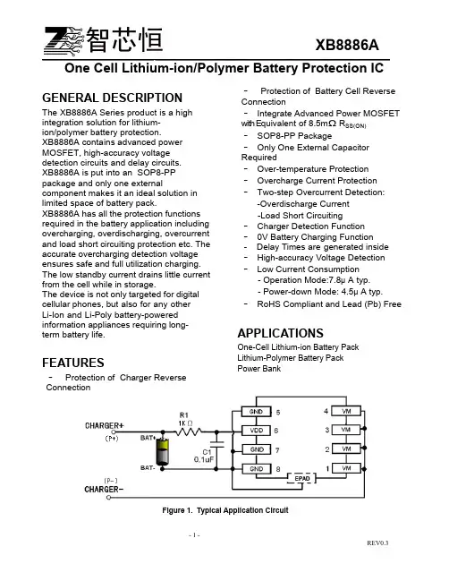
XB8886A ______________________________________ ________________________________________________________________________________ One Cell Lithium-ion/Polymer Battery Protection ICGENERAL DESCRIPTIONThe XB8886A Series product is a high integration solution for lithium-ion/polymer battery protection.XB8886A contains advanced power MOSFET, high-accuracy voltage detection circuits and delay circuits.XB8886A is put into an SOP8-PP package and only one external component makes it an ideal solution in limited space of battery pack.XB8886A has all the protection functions required in the battery application including overcharging, overdischarging, overcurrent and load short circuiting protection etc. The accurate overcharging detection voltage ensures safe and full utilization charging. The low standby current drains little current from the cell while in storage.The device is not only targeted for digital cellular phones, but also for any otherLi-Ion and Li-Poly battery-powered information appliances requiring long-term battery life.FEATURES·Protection of Charger Reverse Connection·Protection of Battery Cell Reverse Connection·Integrate Advanced Power MOSFET with Equivalent of 8.5mΩ R SS(ON)·SOP8-PP Package·Only One External Capacitor Required·Over-temperature Protection ·Overcharge Current Protection ·Two-step Overcurrent Detection: -Overdischarge Current-Load Short Circuiting·Charger Detection Function·0V Battery Charging Function- Delay Times are generated inside ·High-accuracy Voltage Detection ·Low Current Consumption- Operation Mode:7.8μA typ.- Power-down Mode: 4.5μA typ. ·RoHS Compliant and Lead (Pb) FreeAPPLICATIONSOne-Cell Lithium-ion Battery PackLithium-Polymer Battery PackPower BankFigure 1. Typical Application CircuitORDERING INFORMATIONNote: “YW ” is manufacture date code, “Y ” means the year, “W ” means the weekPIN CONFIGURATIONFigure 2. PIN ConfigurationPIN DESCRIPTIONABSOLUTE MAXIMUM RATINGS(Note: Do not exceed these limits to prevent damage to the device. Exposure to absolute maximum rating conditions for long periods may affect device reliability.)ELECTRICAL CHARACTERISTICSTypicals and limits appearing in normal type apply for T A= 25o C, unless otherwise specifiedThe parameter is guaranteed by design.Figure 3. Functional Block DiagramFUNCTIONAL DESCRIPTIONThe XB8886A monitors the voltage andcurrent of a battery and protects it frombeing damaged due to overcharge voltage,overdischarge voltage, overdischargecurrent, and short circuit conditions bydisconnecting the battery from the loador charger. These functions are required inorder to operate the battery cell withinspecified limits.The device requires only one externalcapacitor. The MOSFET is integrated andits R SS(ON) is as low as8.5mΩtypical.Normal operating modeIf no exception condition is detected, charging and discharging can be carried out freely. This condition is called the normal operating mode.Overcharge ConditionWhen the battery voltage becomes higher than the overcharge detection voltage (V CU) during charging under normal conditionand the state continues for the overcharge detection delay time (t CU) or longer, theXB8886A turns the charging control FEToff to stop charging. This condition is called the overcharge condition. The overcharge condition is released in the following two cases:1, When the battery voltage drops below the overcharge release voltage (V CL), the XB8886A turns the charging control FETon and returns to the normal condition.2, When a load is connected and discharging starts, the XB8886A turns the charging control FET on and returns to the normal condition. The release mechanism is as follows: the discharging current flows through an internal parasitic diode of the charging FET immediately after a load is connected and discharging starts, and the VM pin voltage increases about 0.7 V (forward voltage of the diode) from the GND pin voltage momentarily. TheXB8886A detects this voltage and releases the overcharge condition. Consequently, in the case that the battery voltage is equal to or lower than the overcharge detection voltage (V CU), the XB8886A returns to the normal condition immediately, but in the case the battery voltage is higher than the overcharge detection voltage (V CU),the chip does not return to the normal conditionuntil the battery voltage drops below the overcharge detection voltage (V CU) even if the load is connected. In addition, if the VM pin voltage is equal to or lower than the overcurrent detection voltage when a load is connected and discharging starts, the chip does not return to the normal condition.Remark If the battery is charged to a voltage higher than the overcharge detection voltage (V CU) andthe battery voltage does not drops below the overcharge detection voltage (V CU) even when a heavy load, which causes an overcurrent, is connected, the overcurrent do not work until the battery voltage drops below the overcharge detection voltage (V CU). Since an actual battery has, however, an internal impedance of several dozens of mΩ, and the battery voltage drops immediately after a heavy load which causes an overcurrent is connected, the overcurrent work. Detection of load short-circuiting works regardless of the battery voltage.Overdischarge ConditionWhen the battery voltage drops below the overdischarge detection voltage (V DL) during discharging under normal condition and it continues for the overdischarge detection delay time (t DL) or longer, theXB8886A turns the discharging control FET off and stops discharging. This condition is called overdischarge condition. After the discharging control FET is turned off, the VM pin is pulled up by the R VMD resistorbetween VM and VDD in XB8886A. Meanwhile when VM is bigger than 1.5V (typ.) (the load short-circuiting detection voltage), the current of the chip is reduced to the power-down current (I PDN). This condition is called power-down condition. The VM and VDD pins are shorted by theR VMD resistor in the IC under the overdischarge and power-down conditions. The power-down condition is released when a charger is connected and the potential difference between VM and VDD becomes 1.3 V (typ.) or higher (load short-circuiting detection voltage). At this time, the FET is still off. When the battery voltage becomes the overdischarge detection voltage (V DL) or higher (see note),the XB8886A turns the FET on and changes to the normal condition from the overdischarge condition.Remark If the VM pin voltage is no less than the charger detection voltage (V CHA), when the battery under overdischarge condition is connected to a charger, the overdischarge condition is released (the discharging control FET is turned on) as usual, provided that the battery voltage reaches the overdischarge release voltage (V DU) or higher. Overcurrent ConditionWhen the discharging current becomes equal to or higher than a specified value (the VM pin voltage is equal to or higher than the overcurrent detection voltage) during discharging under normal condition and the state continues for the overcurrent detection delay time or longer, theXB8886A turns off the discharging control FET to stop discharging. This condition is called overcurrent condition. (The overcurrentincludes overcurrent, or load short-circuiting.)The VM and GND pins are shorted internally by the R VMS resistor under the overcurrent condition. When a load is connected, the VM pin voltage equals the VDD voltage due to the load.The overcurrent condition returns to the normal condition when the load is released and the impedance between the B+ and B- pins becomes higher than the automatic recoverable impedance. When the load is removed, the VM pin goes back to the GND potential since the VM pin is shorted the GND pin with the R VMS resistor. Detecting that the VM pin potential is lower than the overcurrent detection voltage(V IOV1), the IC returns to the normal condition.Abnormal Charge Current DetectionIf the VM pin voltage drops below the charger detection voltage (V CHA) during charging under the normal condition and it continues for the overcharge detection delay time (t CU) or longer, the XB8886A turns the charging control FET off and stops charging. This action is called abnormal charge current detection. Abnormal charge current detection works when the discharging control FET is on and the VM pin voltage drops below the charger detection voltage (V CHA). When an abnormal charge current flows into a battery in the overdischarge condition, the XB8886A consequently turns the charging control FET off and stops charging after the battery voltage becomes the overdischarge detection voltage and the overcharge detection delay time (t CU) elapses.Abnormal charge current detection is released when the voltage difference between VM pin and GND pin becomes lower than the charger detection voltage (V CHA) by separating the charger. Since the 0 V battery charging function has higher priority than the abnormal charge current detection function, abnormal charge current may not be detected by the product with the 0 V battery charging function while the battery voltage is low.Load Short-circuiting conditionIf voltage of VM pin is equal or below short circuiting protection voltage (V SHORT), the XB8886A will stop discharging and battery is disconnected from load. The maximum delay time to switch current off is t SHORT. This status is released when voltage of VM pin is higher than short protection voltage (V SHORT), such as when disconnecting the load.Delay CircuitsThe detection delay time for overdischarge current 2 and load short-circuiting startswhen overdischarge current 1 is detected.As soon as overdischarge current 2 or load short-circuiting is detected over detection delay time for overdischarge current 2 or load short- circuiting, the XB8886A stops discharging. When battery voltage falls below overdischarge detection voltage due to overdischarge current, the XB8886A stop discharging by overdischarge current detection. In this case the recovery of battery voltage is so slow that if battery voltage after overdischarge voltage detection delay time is still lower than overdischarge detection voltage, the XB8886A shifts to power-down.Figure 4. Overcurrent delay time0V Battery Charging Function (1) (2) (3)This function enables the charging of a connected battery whose voltage is 0 V by self-discharge. When a charger having 0 V battery start charging charger voltage(V0CHA) or higher is connected between B+ and B- pins, the charging control FET gate is fixed to VDD potential. When the voltage between the gate and the source of the charging control FET becomes equal to or higher than the turn-on voltage by the charger voltage, the charging control FET is turned on to start charging. At this time, the discharging control FET is off and the charging current flows through the internal parasitic diode in the discharging control FET. If the battery voltage becomes equal to or higher than the overdischarge release voltage (V DU), the normal condition returns. Note(1) Some battery providers do not recommend charging of completely discharged batteries. Please refer to battery providers before the selection of 0 V battery charging function.(2) The 0V battery charging function has higher priority than the abnormal charge current detection function. Consequently, a product with the 0 V battery charging function charges a battery and abnormal charge current cannot be detected during the battery voltage is low (at most 1.8 V or lower).(3) When a battery is connected to the IC for the first time, the IC may not enter the normal condition in which discharging is possible. In this case, set the VM pin voltage equal to the GND voltage (short the VM and GND pins or connect a charger) to enter the normal condition.TIMING CHART1.Overcharge and overdischarge detectionV V CU -V V DL +V V DL ONONCHARGEV DDV ov1V SS V VMFigure5-1 Overcharge and Overdischarge Voltage Detection2.Overdischarge current detectionV CU V CU -V HC V DL +V DH V DLONDISCHARGEOFFV DDV V ov2V ov1V SS(1)(4)(1)(1)(1)(4)(4)Figure5-2 Overdischarge Current DetectionRemark: (1) Normal condition (2) Overcharge voltage condition (3) Overdischarge voltage condition (4)Overcurrent conditionXB8886A ______________________________________ ____________________________________________________ ___________________________ 3.Charger DetectionVV CU-VV DL+VV DLONV DDVMV SSVFigure5-3 Charger Detection4.Abnormal Charger DetectionVV CU-VV DL+VV DLONONCHARGEV DDVMV SSVFigure5-4 Abnormal Charger DetectionRemark: (1) Normal condition (2) Overcharge voltage condition (3) Overdischarge voltage condition (4)Overcurrent condition)XB8886A ______________________________________ ____________________________________________________ ___________________________ TYPICAL APPLICATIONAs shown in Figure 6, the bold line is the high density current path which must be kept as short as possible. For thermal management, ensure that these trace widths are adequate. C1& R1 is a decoupling capacitor & resistor which should be placed as close as possible toXB8886A.Fig 6 XB8886A in a Typical Battery Protection CircuitPrecautions• Pay attention to the operating conditions for input/output voltage and load current so that the power loss in XB8886A does not exceed the power dissipation of the package.• Do not apply an electrostatic discharge to this XB8886A that exceeds the performance ratings of the built-in electrostatic protection circuit.XB8886A ______________________________________ ____________________________________________________ ___________________________ - 11 -REV0.3 PACKAGE OUTLINE SOP8-EPAD PACKAGE OUTLINE AND DIMENSIONSIn order to increase the driver current capability of XB8886A and improve the temperature of package, Please ensure Epad and enough ground PCB to release energy.。
单节锂电池保护芯片锂电池是一种重要的电池,广泛应用于手机、电动车和便携式电子设备等领域。
为了保证锂电池的安全和性能,需要使用单节锂电池保护芯片对锂电池进行保护。
单节锂电池保护芯片是一种集成电路,主要用于监测锂电池的电压、电流和温度,并在必要时采取措施保护锂电池。
保护芯片通常由主控芯片、保护单元、电源管理单元和通信接口等组成。
主控芯片是单节锂电池保护芯片的核心部件,负责控制和协调保护单元、电源管理单元和通信接口的工作。
主控芯片能够实时监测锂电池的电压、电流和温度,并根据设定的阈值进行判断和控制。
保护单元是单节锂电池保护芯片的关键部件,负责监测锂电池的电压和电流,并在必要时采取措施进行保护。
保护单元可以通过切断电路、放电保护和过压保护等方式来保护锂电池,避免发生过放电、过充电和短路等危险情况。
电源管理单元是单节锂电池保护芯片的重要组成部分之一,用于管理锂电池的充放电过程。
电源管理单元可以通过控制充电电流和放电电流来保护锂电池,并且可以实现恒流充电和恒压充电等充电模式,提高锂电池的充电效率和充电质量。
通信接口是单节锂电池保护芯片的重要功能之一,用于与外部设备进行通信和数据传输。
通过通信接口,可以实现对锂电池的状态监测和控制,以及对充电器和电池管理系统的通信和控制。
单节锂电池保护芯片具有多种保护功能,可以有效地保护锂电池的安全和性能。
首先,它可以监测锂电池的电压,当电压超出设定的范围时,可以及时切断电路,避免电压过高或过低导致锂电池损坏。
其次,它可以监测锂电池的电流,当电流异常时,可以及时采取措施,避免电流过大导致锂电池过热。
此外,单节锂电池保护芯片还可以监测锂电池的温度,并在必要时控制充电或放电,避免温度过高引发火灾等安全问题。
总之,单节锂电池保护芯片是一种重要的电子元器件,可以有效地保护锂电池的安全和性能。
在使用锂电池的电子设备中,应该广泛应用单节锂电池保护芯片,以提高锂电池的使用寿命和安全性。
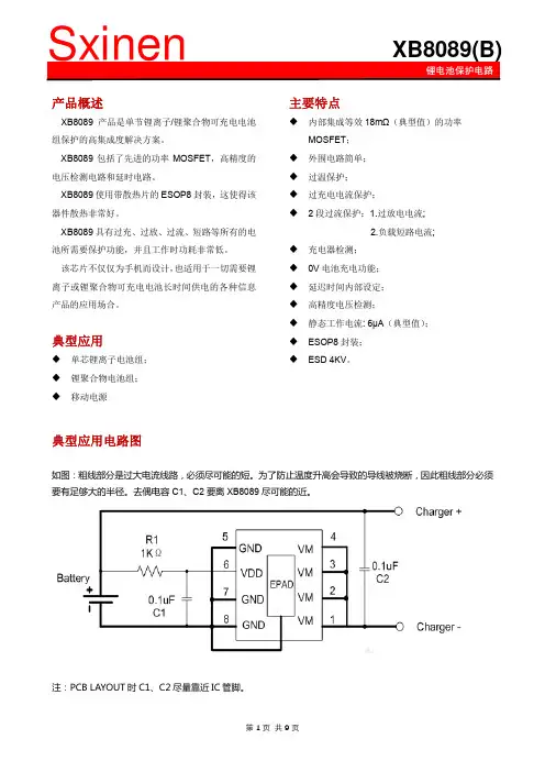
产品概述XB8089产品是单节锂离子/锂聚合物可充电电池组保护的高集成度解决方案。
XB8089包括了先进的功率MOSFET ,高精度的电压检测电路和延时电路。
XB8089使用带散热片的ESOP8封装,这使得该器件散热非常好。
XB8089具有过充、过放、过流、短路等所有的电池所需要保护功能,并且工作时功耗非常低。
该芯片不仅仅为手机而设计,也适用于一切需要锂离子或锂聚合物可充电电池长时间供电的各种信息产品的应用场合。
典型应用◆ 单芯锂离子电池组; ◆ 锂聚合物电池组; ◆ 移动电源主要特点◆ 内部集成等效18m Ω(典型值)的功率MOSFET ; ◆ 外围电路简单; ◆ 过温保护; ◆ 过充电电流保护;◆ 2段过流保护:1.过放电电流;2.负载短路电流;◆ 充电器检测; ◆ 0V 电池充电功能; ◆ 延迟时间内部设定; ◆ 高精度电压检测;◆ 静态工作电流: 6μA (典型值); ◆ ESOP8封装; ◆ ESD 4KV 。
典型应用电路图如图:粗线部分是过大电流线路,必须尽可能的短。
为了防止温度升高会导致的导线被烧断,因此粗线部分必须要有足够大的半径。
去偶电容C1、C2要离XB8089尽可能的近。
注:PCB LAYOUT 时C1、C2尽量靠近IC管脚。
智芯恒参考价:0.03X引脚定义电路内部结构框图注意:1.注意输入输出电压和负载电流情况,保证芯片功耗不超过封装所承受的最大功耗。
2.本产品具有防静电保护功能,但不要超过产品最大的承受静电能力。
典型参数(除非特别指定,T A =25℃)参数 符号 测试条件 最小典型最大值 单位检测电压过充电检测电压CUV-- 4.25 4.3 4.35 V过充电释放电压CLV-- 4.05 4.1 4.15 V过放电检测电压DLV-- 2.3 2.4 2.5 V过放电释放电压DRV-- 2.9 3.0 3.1 V充电器检测电压CHAV-- -0.12 V检测电流过放电电流检测11IOVI Vdd=3.5V 8 A负载短路检测电流SHORTI Vdd=3.5V 40 A静态电流正常工作电流 OPEI Vdd=3.5V, 6 12 uA待机状态电流 PDNI Vdd=2V,VMfloating 3 uA开关管导通阻抗等效导通阻抗 DSR Vdd=3.6V,18 mΩ过温保护过温保护 120 ℃过温恢复 100 ℃迟延时间过充电检测迟延时间CUT VDD=3.6V~4.4V 150 ms过放电检测迟延时间DLT VDD=3.6V~2.0V 35 ms过电流1检测迟延时间1IOVT VDD=3.6V 8 ms负载短路电流检测延迟时间SHORTT VDD=3.6V 70 us 极限参数(注意:不要超过这些参数以免对器件造成损坏,长期超出工作范围条件时会影响器件的可靠性)参数 参数范围 单位 VDD管脚输入电压 -0.3~6 VVM管脚输入电压 -4~8 V工作温度 -40~+85 ℃最大结温度 125 ℃存储温度 -55-150 ℃ 焊接温度(10秒) 260 ℃功耗(25℃) 0.625 W封装热阻(θJA) 100 ℃/W封装热阻(θJC) 130 ℃/WESD 2000 V功能及参数XB8089监控电池的电压和电流,并通过断开充电器或负载,保护单节可充电锂电池不会因为过充电压,过放电压,过充电流,过放电流以及短路等情况而损坏。
Protection IC for 1-Cell Battery PackFeaturesHigh Detection AccuracyOvercharge Detection: ±25mVOverdischarge Detection: ±50mVDischarge Overcurrent Detection: ±15mVCharge Overcurrent Detection: ±30mV High Withstand VoltageAbsolute maximum ratings: 28V(V- pin and CO pin)Ultra Small PackageSOT-23-6 DescriptionThe 8261 is the 1-cell protection IC for lithium-ion/lithium-polymer rechargeable battery pack. The high accuracy voltage detector and delay time circuits are built in 8261 with state-of-art design and process.To minimize power consumption, 8261 activates power down mode when an overdischarge event is detected (for power-down mode enabled version). Besides, 8261 performs protection functions with four external components for miniaturized PCB.The tiny package is especially suitable for compact portable device, i.e. slim mobile phone and Bluetooth earphone.ApplicationMobile phone battery packsDigital camera battery packsBluetooth earphone Li-ion battery module Typical Application CircuitPackage and Pin DescriptionOrdering Information Marking InformationPin No. Symbol pin Description1 DO Connection of discharge control FET gate2 V-Voltage detection between V- pin and VSS pin(Overcurrent / charger detection pin)3 CO Connection of charge control FET gate4 NC No connection5 V DD Connection for positive power supply input6 V SS Connection for negative power supply inputVersion codeSOT-23-61 2 36 5 41) ~ 3) : Version codeProduct version code:8261 OverchargeDetectionVoltageV DET1 (V)OverchargeReleaseVoltageV REL1 (V)OverdischargeDetectionVoltageV DET2 (V)OverdischargeRelease VoltageV REL2 (V)OvercurrentDetectionVoltage V DET3 (V)0V BatteryCharge FunctionPower downmodeFunctionG3P 4.200 4.100 2.750 2.850 0.150 Unavailable Yes G2J 4.325 4.125 2.500 2.900 0.150 Unavailable Yes G3J 4.280 4.080 3.000 3.000 0.080 Available Yes G2N 4.275 4.175 2.300 2.400 0.100 Available Yes Remark Please contact our sales office for the products with detection voltage value other than those specified above.Absolute Maximum RatingsSymbol Descriptions RatingUnits V DDSupply Voltage -0.3 to 7V V-V- pin V DD - 28 to V DD + 0.3 V V COCO pin V DD -28 to V DD + 0.3 V V DOOutput VoltageDO pin Vss - 0.3 to V DD + 0.3VP D Power Dissipation SOT23-6250 mW T OPTOperating Temperature Range -40 to +85 °C T STGStorage Temperature Range -55 to +125°CApplying any over “Absolute Maximum Ratings” practice can permanently damage the device. These data are indicated the absolute maximum values only but not implied any operating performance.Electrical CharacteristicsSymbolItem Conditions MIN TYP MAX UnitDetection VoltageV DET1 Overcharge detection voltage -- V DET1-0.025 V DET1 V DET1+0.025VV REL1 Overcharge release voltage V DET1 ≠ V REL1V REL1-0.05 V REL1 V REL1+0.05 V V DET2 Over-discharge detection voltage -- V DET2-0.05 V DET2 V DET2+0.05 V V REL2 Over-discharge release voltage V DET2 ≠ V REL2 V REL2-0.10 V REL2 V REL2+0.10 V V DET3 Discharge overcurrent detection voltageV DD =3.5V V DET3-0.015 V DET3V DET3+0.015VV DET4 Charge overcurrent detection V DD =3.5V -0.13 -0.10 -0.07 V V SHORTLoad short-circuiting detection voltageV DD =3.5V0.30 0.50 0.70 VDetection Delay Time- 0.96 1.2 1.4 sVDD=4.28V , C ISS =1200pF ,V TH =0.6V0.96 1.22 1.42 s t VDET1* Output delay time of overchargeVDD=4.28V , C ISS =1200pF ,V TH =0.4V0.95 1.23 1.43 s V DET2 >2.5V 120 150 180 ms t VDET2 Output delay time of overdischarge V DET2 ≦2.5V 100 150 200 ms V DET2 >2.5V 7.2 9 11 ms t VDET3Output delay time of discharge overcurrent V DET2 ≦2.5V 6 9 12 ms t SHORTOutput delay time of Load short-circuiting detectionV DD =3.5V 240 300 360μs V DD = 3.5V 7.2 9 11 msV DD =3.5V ,C ISS =1200pF , V TH =0.6V 15.1 19.5 23.8 ms t VDET4*Output delay time of charge overcurrentV DD =3.5V ,C ISS =1200pF , V TH =0.4V16.8 21.6 26.4 ms(Ta = 25o C)(Continued)Symbol Item ConditionsMINTYPMAXUnitCurrent Consumption (power-down function enabled)V DD Operating input voltage V DD - V SS 2.2 6.0VI DD Supplycurrent V DD= 3.5V,V-=0V 1.0 3.0 5.5 μAI STANDBY Power-down current (power-downfunction enabled IC only)V DD=2.0V, V- floating 0.2 μA0V battery Charging FunctionV0CHA 0 V battery charge starting chargervoltage0 V battery chargingfunction “available”1.0 VV0INH 0V battery charge inhibition batteryvoltage0 V battery chargingfunction “unavailable”(Vcharger=4V~14V)0.3 VOutput ResistanceR COH CO pin H resistance V CO=3.0V, V DD=3.5V,V-=0V- 5 10KΩR COL CO pin L resistance V CO=0.5V, V DD=4.5V,V-=0V- 5 10MΩR DOH DO pin H resistance V DO=3.0V, V DD=3.5V,V-=0V- 5 10KΩR DOL DO pin L resistance V DO=0.5V, V DD=1.8V,V-=0V- 5 10KΩV- internal ResistanceR VMD Internal resistance between V- andV DDV DD= 1.8V,V-=0V 100 300 900 KΩR VMS Internal resistance between V- andV SSV DD= 3.5V,V-= 1.0V 100 200 400 KΩ*: Please note that a N-channel MOSFET“turning off delay time”will be affected by 1.Input capacitance (C ISS). 2.Gate threshold voltage (V TH); It causes the delay times of overcharge (tV DET1) and charge overcurrent (tV DET4) of 8261 are prolonged approximately “10ms” to turn off the N-channel MOSFETs to cutting off the current flowing path.Test CircuitsOvercharge, overdischarge and the release detection voltages (test circuit 1)1) Set V1=3.5V, V2=0V, S1=ON and S2=OFF, then 8261 enters operating mode.2) Increase V1 voltage (from 3.5V) gradually. The V1 voltage is the overcharge detection voltage (V DET1)when CO pin goes low (from high).3) Decrease V1 gradually. The V1 voltage is the overcharge release detection voltage (V REL1) when CO pingoes high again.4) Continue decreasing V1. The V1 voltage is the overdischarge detection voltage (V DET2) when DO pin goeslow. Then increase V1 gradually. The V1 voltage is the overdischarge release detection voltage (V REL2), when DO pin returns to high.Note: The overcharge and overdischarge release voltages are defined in versions.Discharge overcurrent detection voltage (test circuit 1)1) Set V1=3.5 V, V2=0V, S1=ON and S2=OFF and XY8261 enter operating condition.2) Increase V2 (from 0V) gradually. The V2 voltage is the discharge overcurrent detection voltage (V DET3)when DO pin goes low (from high).Charge overcurrent detection voltage (test circuit 1)1) Set V1=3.5V, V3=0V, S1=OFF and S2=ON and XY8261 enter operating condition.2) Increase V3 gradually. The V3 voltage is the charge overcurrent detection voltage (V DET4) when CO pingoes low (from high).Load short-circuiting detection voltage (test circuit 1)1) Set V1=3.5V, V2=0V, S1=ON and S2=OFF and 8261 enter operating condition.2) Increase V2 immediately (within 10uS) till DO pin goes “low” from high with a delay time which isbetween the minimum and the maximum of Load short-circuiting delay time.Overcharge, overdischarge delay time (test circuit 1)1) Set V1=3.5V, V2=0V, S1=ON and S2=OFF to enter operating condition.2) Increase V1 from V DET1-0.2V to V DET1+0.2V immediately (within 10us). The overcharge detection delaytime (t VDET1) is the period from the time V1 gets to V DET1+0.2V till CO pin switches from high to low. 3) Set V1=3.5V, V2=0V, S1=ON and S2 = OFF to enter operating condition.4) Decrease V1 from V DET2+0.2V to V DET2-0.2V immediately (within 10us). The overdischarge detection delaytime (t VDET2) is the period from the time V1 gets to V DET2-0.2V till DO pin switches from high to low.Discharge overcurrent delay time (test circuit 1)1) Set V1=3.5V, V2=0V, S1=ON and S2=OFF to enter operating condition.2) Increase V2 from 0V to 0.25V immediately (within 10us). The discharge overcurrent detection delay time(t VDET3) is the period from the time V2 gets to 0.25V till DO pin switches from high to low.Charge overcurrent delay time (test circuit 1)1) Set V1=3.5V, V3=0V, S1=OFF and S2=ON to enter operating condition.2) Increase V3 from 0V to 0.3V immediately (within 10us). The charge overcurrent detection delay time(t VDET4) is the period from the time V3 gets to 0.3V till CO pin gets to low from high.8261高精度单节锂电保护芯片Load short-circuiting delay time (test circuit 1)1)Set V1=3.5V, V2=0V, S1=ON and S2=OFF to enter operating condition.2)Increase V2 from 0V to 1.6V immediately (within 10us). The Load short-circuiting detection voltage delaytime (t SHORT) is the period from the time V2 gets to 1.6V till DO pin switches from high to low.Operating & power down current consumption (test circuit 2)1)Set V1=3.5V, V2=0V and S1=ON to enter operating condition and measure the current I1. I1 is theoperating condition current consumption (I DD).2)Set V1=V2=1.5V and S1=ON enter overdischarge condition and measure current I1. I1 is the powerdown current consumption (I STANDBY).Resistance between V- and V DD, V- and V SS (test circuit 2)1)Set V1=1.8V, V2=0V and S1=ON and XY8261 enters overdischarge condition. V1/I1 is the internalresistance between V- and VDD pin (R VMD).2)Set V1=3.5V, V2=1.0V and S1=ON and XY8261 enters discharge overcurrent condition. V2/I2 is theinternal resistance between V- and V SS pin (R VMS).Output resistance (test circuit 3)1)Set V1=3.5V, V2=0V, V3=3.0V, S1=OFF and S2=ON to enter operating condition. (V3-V1)/I2 is theinternal resistance (R COH).2)Set V1=4.5V, V2=0V, V3 =0.5V, S1=OFF and S2=ON to enter overcharge condition. V3/I2 is the internalresistance (R COL).3)Set V1=3.5V, V2=0V, V3=3.0V, S1=ON and S2=OFF to enter operating condition. (V3-V1)/I2 is theinternal resistance (R DOH).4)Set V1=1.8 V, V2=0V, V3 =0.5V, S1=ON and S2=OFF to enter overdischarge condition. V3/I2 is theinternal resistance (R DOL).0V battery charge starting charger voltage (products with 0V battery charging function is “Available”) (test circuit 4)1)Set V1=V2=0V, increase V2 gradually.2)The V1 voltage is the 0V charge inhibition voltage (V0INH) when CO pin switches from low to high (V V- +0.1V or higher).0V battery charge inhibition battery voltage (products with 0V battery charging function is “Unavailable”) (test circuit 4)1)Set V1=0V, V2=4V and increase V1 gradually.2)The V1 voltage is the 0V charge inhibition voltage (V0INH) when CO pin switches from low to high (V V- +0.1V or higher).Note: The charger voltage should not be higher than 14V of 0V battery charge inhibition battery voltage.Recommended:1) '0 V charge available' doesn't means 8261 can reco ver the zero-V cell to be full charged if this cell hasbeen already damaged due to too low voltage.2) In 8261, the '0 V charge inhibition' voltage is rather lower (0.3V~0.5V). That is, 8261 allowscharging such low voltage cell and recover it.3) For safety consideration, we strongly recommended to select '0 V charge inhibition' to prevent fromcharging a damaged cell.TestCircuitTest circuit 1 Test circuit 2Test circuit 4Test circuit 3OperationThe 8261 provides overcharge, overdischarge, discharge overcurrent, charge overcurrent and loadshort-circuiting protections for the 1-cell battery pack. 8261 continuously monitors the voltage of battery between V DD pin and VSS pin to control overcharge and overdischarge protections. When the battery pack is in charging stage, the current flows from the charger to the battery through EB+ and EB-; the voltage between V- pin and VSS pin is negative. On the other hand, when the battery pack is in discharging stage, the current flows from battery to the load through EB+ and EB-; the voltage between V- pin and VSS pin is positive. The 8261 also monitors the voltage which is determined by the current of charge and discharge and the series Rds(on) of MOSFETs between V- pin and V SS pin to detect charge overcurrent and discharge overcurrent current conditions. (1) Normal Condition (Operation mode)The 8261 turns both the charging and discharging control MOSFETs on when the voltage of battery is in the range from overcharge detection voltage (V DET1) to overdischarge detection voltage (V DET2), and the VM pin voltage is in the range from overcurrent detection voltage (V DET4) to discharge overcurrent detection voltage (V DET3). This is called the normal condition that charging and discharging can be carried out freely.Caution: The XY8261 may be needed connecting a charger to return to normal condition, when the batteryis connected for the first time.(2) Overcharge Condition1) Overcharge Protection:When the V DD voltage is higher than the overcharge detection voltage (V DET1) and lasts for longer than the overcharge detection delay time (t VDET1), 8261 turns off the external charging MOSFET to protect the pack from being overcharged, which CO pin turns to “L” from “H” level. 2) Overcharge Protection Release:When the battery voltage is lower than V REL1 and the V- pin voltage is between charge overcurrent detection voltage (V DET4) and discharge overcurrent detection voltage (V DET3), the XY8261 would release this condition.When the battery voltage is lower than V DET1 and charger is removed, the 8261 can be released from this condition. (3) Overdischarge Condition1) Overdischarge Protection:When the V DD voltage is lower than the overdischarge detection voltage (V DET2) and lasts longer than overdischarge detection delay time (t VDET2), 8261 turns off the external discharge MOSFET to protect the pack from being overdischarged, which DO pin turns to “L” from “H” level. In overdischarge condition V- pin is pulled-up to V DD by a resistor (R VMD ) between the V- pin and V DD pin. After that, when V- pin voltage is higher than V DD /2(Typ), the IC gets to power down mode. 2) Overdischarge Protection Release:The overdischarge protection is released when(a) a charger is connected and V- pin voltage is lower than -0.7V (Typ.) and battery voltage is higher thanthe overdischarge voltage, or8261高精度单节锂电保护芯片(b)a charger is connected, and V- pin voltage is higher than –0.7V (Typ.) and battery voltage is higherthan the overdischarge release voltage.(4) Discharge Overcurrent Condition1) Discharge Overcurrent Protection:The 8261 provides discharge overcurrent protection and load short-circuiting protection:(a) Discharge overcurrent protection occurs when V- pin voltage between V DET3 and V SHORT and lasts for acertain delay time (t VDET3) or longer .(b) Load short-circuiting protection occurs when V- pin voltage higher than V SHORT and lasts for a certaindelay time (t SHORT ) or longer .When above conditions happen, the DO pin goes “L” from ”H” to turn off the discharging MOSFET .In discharge overcurrent and load short-circuiting conditions, V- pin is pulled-down to V SS pin by the internal resistor (R VMS ). 2) Discharge Overcurrent and Load Short-Circuiting Protection Release:The IC detects the status by monitoring V- pin voltage that is inversely proportional to the impedance (Rload) between two terminals (EB+ and EB-). The Rload increases while the V- pin voltage decreases. When the V- pin voltage equals to V SHORT or lower , discharge overcurrent status returns to normal mode. The relation between V- and Rload is shown as follows:(5) Charge Overcurrent ConditionThe 8261 provides charge overcurrent protection to prevent the battery pack from being connected to an unexpected charger .1) Charge Overcurrent ProtectionWhen the voltage of V- pin is lower than charge overcurrent detection voltage (V DET4) and lasts for a certain delay time (t DET4) or longer , the CO pin goes “L” from ”H” to turn off the charging MOSFET . 2) Charge Overcurrent Release: Charge overcurrent protection can be only released by disconnecting thecharger . (6) Power Down Condition1) Entering to Power Down Mode:8261 enters the power down mode when overdischarge protection occurs and V- pin voltage is higher than V DD /2 (typical). The V- pin voltage is pulled-up to the V DD through the R VMD resistor. The internal circuits is shut off, therefore, the power-down current (I STANDBY ) is reduced to be low 0.2uA (Max.). 2) Power Down Mode Release:The power down mode is released when a charger is connected and V- pin voltage is lower than V DD /2 (typical).Note: Power down condition is for power down mode enabled version only.RVMSRVMS + RloadX VDD V-=; whereV- ≦ Vshort8261高精度单节锂电保护芯片Block DiagramVSS DO V-COVDD(a) Normal condition (b) Overcharge condition (c) Charge overcurrent condition*: The charger is assumed to charge with a constant current.Timing Chart(1) Overcharge, Charge Overcurrent OperationV V V V V V CO pin voltageBattery voltagecurrentCharge/Discharge V-pin voltageV V(2) Overdischarge, Discharge Overcurrent, Load Short-Circuiting Operation(a) Normal condition (b) Overdischarge condition (c) Discharge overcurrent condition (d) Load short-circuit condition*: The charger is assumed to charge with a constant current.BatteryV-Charge/DO pin V tV V V V V tttvoltagepin voltageV V Charge CurrentDischarge currentvoltageVRecommended Application CircuitTable1 Constant for external componentsSymbol Parts Purpose Recommended Min . Max . RemarksFET1N channelMOSFETDischarge control------------*1) 0.4 V < Threshold voltage < Overdischarge detection voltage. Gate to source withstand voltage > Charger voltage.FET2N channel MOSFETCharge control ---- ---- ----*1) 0.4 V < Threshold voltage <Overdischarge detection voltage. Gate to source withstand voltage > Charger voltage.R1 ResistorESD protection for power fluctuation470Ω 240Ω 1K Ω *2) Set Resistance to the value 2R1<R2.C1Capacitor For power fluctuation0.1uF0.022uF1.0uF*3) Install a 0.22uF capacitor or higher .R2 Resistor Protection for reverseconnection of a charger 1K Ω 300Ω 2K Ω *4) The resistor is preventing big current when a charger is connectedin reverse.*1) If the threshold voltage of an FET is lower than 0.4V, the FET may failed to stop the charging current.If an FET has a threshold voltage equal to or higher than the overdischarge detection voltage, discharging may be stopped before overdischarge is detected.If the charger voltage is higher than the withstanding voltage between the gate and source, the FET may be damaged. *2) Employing an over-specification (listed in above table) R1 may result in overcharge detection voltage and release voltagehigher than the defined voltage (listed in page 4)If R1 has a higher resistance, the IC may be damaged caused by over absolute maximum rating of VDD voltage when a charger is connected reversely.EB+EB-*3) Applying a smaller capacitance C1 to system, DO may failed to function when load short-circuiting is detected.*4) If R2 resistance is higher than 2kΩ, the charging current may not be cut when a high-voltage charger is connected.Caution: 1) The above constants may be changed without notice.2) The application circuit above is for reference only. To determine the correct constants,evaluation of actual application is required.Precautions: 1) The application condition for the input voltage, output voltage, and load current should not exceed the package power dissipation.2) Do not apply an electrostatic discharge to this IC that exceeds the performance ratingsof the built-in electrostatic protection circuit.Package InformationSOT-23-6 Dimensionsθ°θ12. Reference: JEDECMO-178AA3. SOT23-5 / SOT23-6。