SX4059-DATASHEET-V1.0(单节锂电池充电管理带锂电保护复合芯片)
- 格式:pdf
- 大小:577.88 KB
- 文档页数:13
公司推出单节锂离子电池线性充电的LY4059系列锂电池充电IC芯片。
LY4059采用小型SO P-8封装锂电池充电IC芯片,以及标准的SOT-25锂电池充电IC芯片和SOT-89-5锂电池充电IC芯片封装,包括有参考电压、电池电压监测、驱动晶体管、恒流/恒压充电电路、过热保护电路、相位补偿电路。
电池充电终端电压内部设定为4.2V,精度为±0.7%,涓流充电电压为2.9V,精度为±3%。
LY4059是一款具有恒流恒压充电模式的锂电池充电管理芯片。
可以对单节(4.2V/4.34)锂电池进行快速高效地充电。
其采用电流模式PWM 降压型开关控制结构,为锂电池快速充电提供了微型、简单且高效的解决方案。
LY4059内置防倒灌功能,所以实际应用不需要输入端接二极管防倒灌。
LY4059由外部Sense 电阻设定出高精度的充电电流,内部由分压电阻和精准的参考电压将电池的浮充电压设定在4.2V/4.34V 同时具有高达±1%的精度。
当输入电源去掉后,芯片会自动进入低电流休眠模式,电池的漏电流低至1μA。
当充电周期结束后,如果单节电池电压降到4.1V/4.15V 后,芯片将自动重新对电池进行充电。
● 输入电压范围: 4.7V-6V● 内置防倒灌功能● 内置软启动,防止上电瞬间的大电流过冲● 高效电流模式PWM降压型开关控制结构● 充电结束时电流检测输出● 采用固定开关频率以保证最小的噪声● ±1%的充电电压(4.2V/4.34V)精度● 自动再充电● 输入电源去除自动进入休眠模式● 电池电压较低时自动进入涓流充电模式● 采用低ESR的陶瓷电容输出稳定● 电池温度检测。
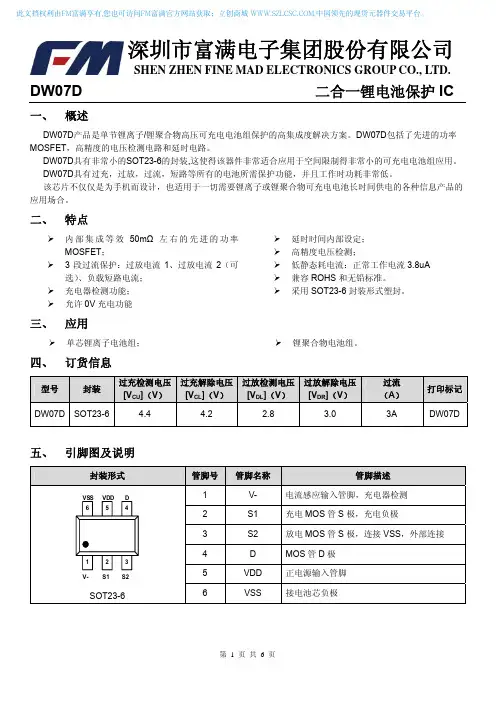
DW07D 二合一锂电池保护IC一、 概述DW07D 产品是单节锂离子/锂聚合物高压可充电电池组保护的高集成度解决方案。
DW07D 包括了先进的功率MOSFET ,高精度的电压检测电路和延时电路。
DW07D 具有非常小的SOT23-6的封装,这使得该器件非常适合应用于空间限制得非常小的可充电电池组应用。
DW07D 具有过充,过放,过流,短路等所有的电池所需保护功能,并且工作时功耗非常低。
该芯片不仅仅是为手机而设计,也适用于一切需要锂离子或锂聚合物可充电电池长时间供电的各种信息产品的应用场合。
二、 特点¾ 内部集成等效50m Ω左右的先进的功率MOSFET ;¾ 3段过流保护:过放电流1、过放电流2(可选)、负载短路电流; ¾ 充电器检测功能; ¾ 允许0V 充电功能¾ 延时时间内部设定; ¾ 高精度电压检测;¾ 低静态耗电流:正常工作电流3.8uA ¾ 兼容ROHS 和无铅标准。
¾采用SOT23-6封装形式塑封。
三、 应用¾ 单芯锂离子电池组;¾ 锂聚合物电池组。
四、 订货信息型号封装过充检测电压 [V CU ](V ) 过充解除电压[V CL ](V )过放检测电压[V DL ](V )过放解除电压 [V DR ](V )过流 (A )打印标记DW07D SOT23-6 4.4 4.2 2.8 3.0 3A DW07D五、 引脚图及说明DW07D二合一锂电池保护IC六、 极限参数参数符号参数范围单位电源电压VDD VSS-0.3~VSS+12 V CSI输入管脚电压VCSI VDD+15~VDD+0.3 V 工作温度Topr -40~+85 ℃存储温度Tstg -40~+125 ℃七、 电气特性参数参数符号测试条件最小值典型值最大值单位工作电压工作电压VDD -- 1.5--10V 电流消耗工作电流IDD VDD= 3.9V --3.06.0 uA检测电压过充电检测电压A档VOCP --4.350 4.375V B档 4.375 4.400 4.425C档 4.425 4.450过充电释放电压VOCR -- 4.15 4.20 4.25 V 过放电检测电压VODP -- 2.72 2.80 2.88 V 过放电释放电压VODR -- 2.92 3.00 3.08 V 过电流1检测电压VOI1 -- 0.12 0.15 0.18 V 过电流2(短路电流)检测电压VOI2 VDD= 3.6V 0.80 1.00 1.20 V 过电流复位电阻Rshort VDD= 3.6V 50100150 KΩ过电器检测电压VCHA -- -0.8 -0.5 -0.2 V 向0V电池充电的功能充电器起始电压V0CH 允许向0V电池充电功能1.2 -- -- V迟延时间过充电检测迟延时间TOC VDD= 3.6V~4.4V -- 110 200 ms过放电检测迟延时间TOD VDD= 3.6V~2.0V -- 80 140 ms过电流1检测迟延时间TOI1 VDD= 3.6V 51320 ms过电流2(短路电流)检测迟延时间TOI2 VDD= 3.6V --550 usMOS参数单个MOS管漏极到源极的导通阻抗R DS(on) V GS = 2.5V, I D =0.5A-- 22.0 30.0 mΩR DS(on) V GS = 4.5V, I D = 1.0A-- 16.0 25.0过流I ODC VDD= 3.6V 2.0 3.0 4.0 A 漏-源击穿电压V(BR)DSS V GS = 0V, I D= 250μA19 20 -- V连续的漏极电流I D(DeviceRef.)T J= 25°C 5 ADW07D二合一锂电池保护IC 栅极阈值电压V GS(th)V DS=VGS, I D=250μA0.55 0.65 0.95 V漏-源极电流I DSS V DS=20V, V GS= 0V,T J= 25°C1 uA栅-源极电流I GSS V GS= ±10V 100 nA 八、功能描述DW07D监控电池的电压和电流,并通过断开充电器或负载,保护单节可充电锂电池不会因为过充电压,过放电压,过放电流以及短路等情况而损坏。
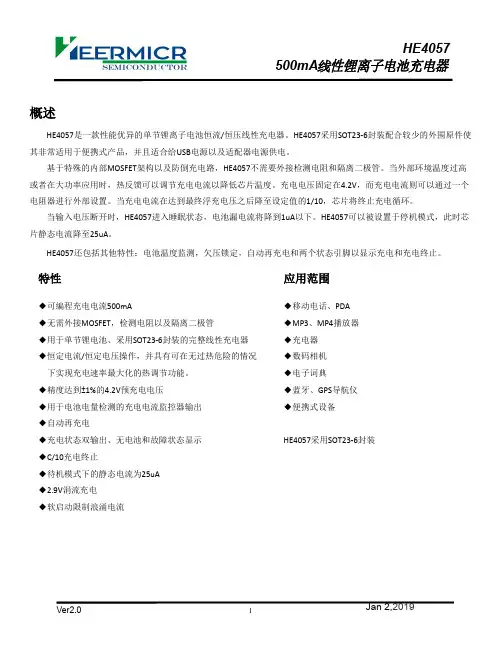
概述HE4057是一款性能优异的单节锂离子电池恒流/恒压线性充电器。
HE4057采用SOT23-6封装配合较少的外围原件使其非常适用于便携式产品,并且适合给USB电源以及适配器电源供电。
基于特殊的内部MOSFET架构以及防倒充电路,HE4057不需要外接检测电阻和隔离二极管。
当外部环境温度过高或者在大功率应用时,热反馈可以调节充电电流以降低芯片温度。
充电电压固定在4.2V,而充电电流则可以通过一个电阻器进行外部设置。
当充电电流在达到最终浮充电压之后降至设定值的1/10,芯片将终止充电循环。
当输入电压断开时,HE4057进入睡眠状态,电池漏电流将降到1uA以下。
HE4057可以被设置于停机模式,此时芯片静态电流降至25uA。
HE4057还包括其他特性:电池温度监测,欠压锁定,自动再充电和两个状态引脚以显示充电和充电终止。
特性◆可编程充电电流500mA◆无需外接MOSFET,检测电阻以及隔离二极管◆用于单节锂电池、采用SOT23-6封装的完整线性充电器◆恒定电流/恒定电压操作,并具有可在无过热危险的情况下实现充电速率最大化的热调节功能。
◆精度达到±1%的4.2V预充电电压◆用于电池电量检测的充电电流监控器输出◆自动再充电◆充电状态双输出、无电池和故障状态显示◆C/10充电终止◆待机模式下的静态电流为25uA◆2.9V涓流充电◆软启动限制浪涌电流应用范围◆移动电话、PDA◆MP3、MP4播放器◆充电器◆数码相机◆电子词典◆蓝牙、GPS导航仪◆便携式设备HE4057采用SOT23-6封装HE4057 500mA线性锂离子电池充电器典型应用打标说明及管脚分布SOT23-6管脚图丝印字符丝印字符说明 左示意图57BM芯片..Y 年号 W 周号 XXXX生产批号管脚描述57BM YWXXXX最大额定值(注)ESD与Latch-up等级结构框图(如果没有特殊说明,环境温度= 25︒C,输入电压=5V)注释(1): 这时处于充电状态,I CC= I VCC- I BAT(2): 这里C/10终止电流门限指的是终止电流与恒流充电电流的比值使用说明HE4057是一款专门为锂离子电池设计的线性充电器,利用芯片内部的功率MOSFET对电池进行恒流/恒压充电。
单节/双节线性锂电池充电芯片规格书1、HT6292功能简述1.1、特性● 完全的单节/两节锂离子/锂聚合物电池充电芯片● 极低的热消耗● 集成MOSFET、内置电流检测● 不需要外接反相保护二极管● 0.8%的充电电压精度● 可编程充电电流控制,最大达600mA● 芯片温度热折返保护● NTC 热敏接口监测电池温度● 有无电池检测● LED充电状态指示● 恒压充电电压值可通过外接电阻微调● 可以配置为单节或双节锂电池充电● 短路检测、保护● USB与AC适配器电压输入可选择● 工作环境温度范围:-30℃~70℃● 小型SSOP-16封装1.2、应用● 手持设备,包括医疗手持设备● PDA,移动蜂窝电话及智能手机● 移动仪器,MP3● 自充电电池组● 独立充电器● USB总线供电充电器1.3、概述HT6292为线性锂离子/锂聚合物电池充电芯片,其最低输入电压可低至3.6伏,最大充电电流可达600mA。
HT6292能够编程设计适应各种AC适配器及USB接口。
电池充电分为恒流(CC/Constant Current)、恒压(CV/Constant Voltage)过程,恒流充电电流通过外部电阻决定,最大为600mA。
如果考虑到热扩散问题时,往往使用限流输出的AC适配器,使用HT6292 则可以兼顾线性充电器、开关型充电的优点:充电快,自耗功率小。
HT6292 集成电流热折返保护电路、短路保护,确保充电芯片安全工作。
HT6292可以检测电池是否过放电,并对过放电的电池进行预充电。
HT6292集成NTC热敏电阻接口,可以采集、处理电池的温度信息,保证充电电池的安全工作温度。
HT6292 采用SSOP-16封装。
2、HT6292功能框图图1、HT6292功能框图3、 管脚定义图2、HT6292管脚分布图表1、HT6292管脚描述序号 符号 I/O 描述1 VTRIM - 外接电阻微调满充电压 2&3 VIN I 输入电源4CELLI0:两节锂电池充电 1或悬空:单节锂电池充电5 GND - 地6PDNI芯片使能输入: 0:芯片不工作 1或悬空:芯片工作7TOENI0:取消充电时间限制1或悬空:使能内部充电时间限制8 FAULT O FAULT(GREEN)STATUS(RED)描述0 0 没有充电或者无电池 0 1 正在充电 1 0 充电完成 0 PULSE1 故障状态 9STATUSOPULSE2电池温度异常10 CREF - 振荡器外接电容,决定内部振荡频率,同时提供参考时钟 11 TEMP I 温度传感信号输入12 V33 O 输出3.3V 参考电压,提供10mA 驱动能力 13VSELI0:USB 输入,充电电流为适配器输入时的50% 1或悬空:适配器输入14 RREF - 外接电阻控制恒流充电电流 15&16 VOUTO输出,接锂电池4、HT6292电气特性和推荐工作条件表2、HT6292推荐工作条件参数 最小值 典型值 最大值单位备注电源电压 4.5 5.0 6.5 V 单节电池充电电源电压8.8 10.0 11 V 双节电池充电环境温度-20 70 ℃5、HT6292性能参数表3、HT6292性能参数(一节电池,Ta=25℃)参数 符号 测试条件 最小 典型 最大 单位 上电复位电压上电复位 VPOR 3.6 V Standby模式VOUT漏电流 VBAT=3.7V 20 uA VIN电源电流VOUT悬空、PDN=0 100 uAVOUT悬空、PDN=1或悬空 1 mA 电压调整输出电压 4.158 4.20 4.242 V Dropout电压 200 mV 充电电流恒流充电电流A Icc VRREF>1.3V、VBAT=3.7V540 600 660 mA 预充电电流A Ipre VRREF>1.3V、VBAT=2.0V75 mA 恒流充电电流B Icc VRREF<0.4V、VBAT=3.7V100 mA 预充电电流B Ipre VRREF<0.4V、VBAT=2.0V12 mA 恒流充电电流C Icc RREF=35K、VBAT=3.7V 600 mA 预充电电流C Ipre RREF=35K、VBAT=2.0V 75 mA 再充电、预充电电压预充电阈值电压 Vpre 2.7 2.8 3.0 V 再充电阈值电压 Vrhg 3.95 V 温度监测低温阈值电压高温阈值电压折返阈值 85 100 115 ℃ 折返电流增益 100 mA/℃ 振荡器振荡频率 CREF=20nF 333 Hz 振荡周期 CREF=20nF 2.4 3.0 3.6 mS 逻辑电平逻辑高电平 VH 2 V 逻辑低电平 VL 0.8 V STATUS/FAULT驱动电流 5 mA表4、HT6292性能参数(双节电池,Ta=25℃)参数 符号 测试条件 最小 典型 最大 单位 上电复位电压上电复位 VPOR 6.4 V Standby模式VOUT漏电流 VBAT=7.4V 40 uA VIN电源电流VOUT悬空、PDN=0 100 uAVOUT悬空、PDN=1或悬空 1 mA 电压调整输出电压 8.316 8.40 8.484 V Dropout电压 200 mV 充电电流恒流充电电流A Icc VRREF>1.3V、VBAT=7.4V540 600 660 mA 预充电电流A Ipre VRREF>1.3V、VBAT=4.0V75 mA 恒流充电电流B Icc VRREF<0.4V、VBAT=7.4V100 mA 预充电电流B Ipre VRREF<0.4V、VBAT=4.0V12 mA 恒流充电电流C Icc RREF=35K、VBAT=7.4V 600 mA 预充电电流C Ipre RREF=35K、VBAT=4.0V 75 mA 再充电、预充电电压预充电阈值电压 Vpre 5.4 5.6 6.0 V 再充电阈值电压 Vrhg 7.9 V 温度监测低温阈值电压高温阈值电压折返阈值 85 100 115 ℃ 折返电流增益 100 mA/℃ 振荡器振荡频率 CREF=20nF 333 Hz 振荡周期 CREF=20nF 2.4 3.0 3.6 mS 逻辑电平逻辑高电平 VH 4 V 逻辑低电平 VL 0.4 V STATUS/FAULT驱动电流 5 mA6、HT6292功能描述及管脚应用说明6.1、锂电池充电介绍图3、锂电池充电曲线示意图锂电池充电过程主要分为恒流充电和恒压充电,恒流充电阶段充电电流保持恒定,同时电池电压不断上升。
1.概述内置高精度电压检测电路和延时电路进行电压、电流以及温度的监控,保证Pack 安全。
此外, 具有0V 充电功能,提升Pack 使用寿命。
具有三种工作模式:正常模式、休眠模式和关机模式。
当任意电芯处于低容量状态时,进入休眠模式来降低系统功耗。
2.特点◆ 高精度电压检测功能:过充电保护电压V OV :3.600V-4.375V (档位25mV) 过充电保护电压精度:±25mV 迟滞电压:0-350mV过放保护电压V UV :2.0V - 3.1V (档 位100mV) 过放电保护电压精度:±80mV 过放电保护解除迟滞电压:0-1.0V◆ 放电过流检测功能:过流1保护电压V DOC1:0.025V - 0.350V (档位25mV) 过流1保护电压精度:±10mV过流2保护电压V DOC2:2×VDOC1 (档位50mV) 过流2保护电压精度:±20mV◆ 短路检测功能:短路保护电压V SC :4.5×VDOC1 (档位112.5mV) 短路保护电压精度:±45mV◆ 温度检测功能:充电高温保护温度:50°C 充电高温保护温度精度:±4℃(Max.) 充电低温保护温度:0°C 充电低温保护温度精度:±4℃(Max.)ZCC8993ZCC8993ZCC8993ZCC8993放电高温保护温度:70°C 放电高温保护温度精度:±4℃(Max.)◆外接电容设置过放电保护延时、放电过流1保护延时以及放电过流2保护延时◆过充电保护延时、短路保护延时以及温度保护延时固定◆工作电压范围:3V - 26V◆工作温度范围:-40℃~85℃◆集成N-MOSFET驱动◆低功耗设计:正常工作功耗:18 uA (Max.)休眠模式功耗:5 uA (Max.)◆封装形式:16-pin TSSOP◆SEL管脚选择3/4串应用3.订购信息注释:目前只有A,B版本VC1VC2VC3VC4VDDGNDSELVI DSGCHG TSCDCDSD CHSEVMTEST图系统框图ZCC8993TEST CHSE CHG VM DSG DSD CDC VIVDDVC1VC2VC3VC4GNDSELTS 管脚图6.管脚定义ZCC89937.功能描述7.1正常模式下列条件均满足时, 处于正常模式:(1) 所有电芯电压位于过充电保护电压 (V OV ) 与过放电保护电压 (V UV ) 之间 (2) VI 管脚电平小于放电过流1保护电压V DOC1(3) TS 管脚检测温度位于充电高温保护温度T COT 与充电低温保护温度T CUT 之间 (4) 无安全保护发生7.2过充电保护状态下列条件均满足时,进入过充电保护状态: (1) 任意电芯电压高于过充电保护电压V OV (2) 状态(1)持续时间超过过充电保护延时t OV 处于过充电保护状态时,CHG 管脚输出高阻态。
南京拓品微电子有限公司NanJing Top Power ASIC Corp.数据手册DATASHEETTP4058(600mA线性锂离子电池充电器)概述、特点、典型应用-------------------------------------------------------------------------------------P2管脚、特性指标----------------------------------------------------------------------------------------------P3引脚功能说明-------------------------------------------------------------------------------------------------P5充电电流大小设置、电池反接保护功能----------------------------------------------------------------P7充电指示状态、无电池连接指示状态-------------------------------------------------------------------P8多种典型应用图、使用注意事项-------------------------------------------------------------------------P12特点·锂电池正负极反接保护;·高达600mA的可编程充电电流;·无需MOSFET、检测电阻器或隔离二极管;·用于单节锂离子电池·恒定电流/恒定电压操作,并具有可在无过热危险的情况下实现充电速率最大化的热调节功能;·可直接从USB端口给单节锂离子电池充电;·最高输入可达9V;·精度达到±1%的4.2V预设充电电压;·自动再充电;·1个充电状态开漏输出引脚;·C/10充电终止;·待机模式下的供电电流为145uA;·2.9V涓流充电;·软启动限制了浪涌电流;·采用5引脚SOT-23封装。
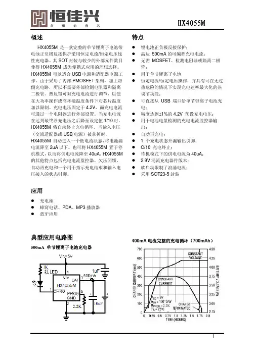
概述HX4055M 是一款完整的单节锂离子电池带电池正负极反接保护采用恒定电流/恒定电压线性充电器。
其SOT 封装与较少的外部元件数目使得HX4055M 成为便携式应用的理想选择。
HX4055M 可以适合USB 电源和适配器电源工作。
由于采用了内部PMOSFET 架构,加上防倒充电路,所以不需要外部检测电阻器和隔离二极管。
热反馈可对充电电流进行调节,以便在大功率操作或高环境温度条件下对芯片温度加以限制。
充电电压固定于4.2V,而充电电流可通过一个电阻器进行外部设置。
当充电电流在达到最终浮充电压之后降至设定值1/10时,HX4055M 将自动终止充电循环。
当输入电压(交流适配器或USB 电源)被拿掉时,HX4055M 自动进入一个低电流状态,将电池漏电流降至2uA 以下。
也可将HX4055M 置于停机模式,以而将供电电流降至40uA 。
HX4055M 的其他特点包括充电电流监控器、欠压闭锁、自动再充电和一个用于指示充电结束和输入电压接入的状态引脚。
应用充电座蜂窝电话、PDA 、MP3播放器 蓝牙应用典型应用电路图500mA 单节锂离子电池充电器特点锂电池正负极反接保护;高达 500mA 的可编程充电电流;无需 MOSFET 、检测电阻器或隔离二极管;用于单节锂离子电池恒定电流/恒定电压操作,并具有可在无过热危险的情况下实现充电速率最大化的热调节功能;可直接从 USB 端口给单节锂离子电池充电;精度达到±1%的4.2V 预设充电电压; 用于电池电量检测的充电电流监控器输出;自动再充电;1 个充电状态开漏输出引脚; C/10 充电终止;待机模式下的供电电流为40uA ; 2.9V 涓流充电器件版本; 软启动限制了浪涌电流; 采用SOT23-5封装400mA 电流完整的充电循电流完整的充电循环环(700mAh )引脚示意图引脚引脚分配分配分配图图引脚序号引脚名称 引脚说明1 CHRG 漏极开路输出的充电状态指示端2 GND 地3 BAT 充电电流输出4 VCC 正输入电源电压5PROG充电电流设定、充电电流监控和停机引脚绝对最大额定值输入电源电压(V CC ).........................................................................................................-0.3V ~9VPROG.....................................................................................................................-0.3V ~V CC +0.3V BAT............................ .....................................................................................................-4.2V ~7V CHRG ...........................................................................................................................-0.3V ~10V BAT 短路持续时间......................................................................................................................连续 BAT 引脚电流.........................................................................................................................500mA PROG 引脚电流.....................................................................................................................800uA 最大结温..................................................................................................................................145℃ 工作环境温度范围. .......................................................................................................-40℃~85℃ 贮存温度范围..............................................................................................................-65℃~125℃ 引脚温度(焊接时间10秒)...................................................................................................260℃电气特性符号参数条件最小值典型值最大值单位VCC 输入电源电压 4.0 5 9.0 VICC 输入电源电流充电模式,RPROG=11K待机模式(充电终止)停机模式(RPROG未连接,VCC<VBAT,或VCC<VUV)150404040500100100100uAVFLOAL 稳定输出(浮充)电压0℃≤TA≤85℃,IBAT=40mA4.158 4.2 4.242 VIBAT BAT引脚电流RPROG=11K,电流模式RPROG=3.6K,电流模式RPROG=2.2K,电流模式待机模式,VBAT=4.2V停机模式(RPROG未连接)睡眠模式,VCC=0V80290480100310500-2.5±1-1120320520-6±2-2mAmAmAuAuAuAITRIKL 涓流充电电流VBAT<VTRIKL,RPROG=11K 10 15 20 mA VTRIKL 涓流充电门限电压RPROG=11K,VBAT 上升 2.75 2.9 3.0 V VTRHYS 涓流充电迟滞电压RPROG=11K 60 80 100 mV VUV VCC欠压闭锁门限从VCC低至高 3.4 3.6 3.8 V VUVHYS VCC欠压闭锁迟滞150 200 300 mVVMSD 手动停机门限电压PROG引脚电平上升PROG引脚电平下降3.401.903.502.003.602.10VVASD VCC-VBAT闭锁门限电压VCC从低到高VCC从高到低6051003014050mVITERM C/10终止电流门限RPROG=11KRPROG=1.66K83010401250mVVPROG PROG引脚电压RPROG=11K,电流模式0.9 1.0 1.1 V ICHRG CHRG 引脚漏电流VCHRG=5V(待机模式)0 1 uA VCHRG CHRG 引脚输出低电压ICHRG=5mA 0.3 0.6 V ∆VRECHRG 再充电电池门限电压VFLOAT-VRECHRG 100 150 200 mV TLIM 限定温度模式中的结温120 ℃RON功率FET“导通”电阻(在VCC与BAT 之间)650 mΩtss 软启动时间IBAT=0至IBAT=1000V/RPROG 20 uS tRECHARGE 再充电比较器滤波时间VBAT高至低0.8 1.8 4 mS tTERM 终止比较器滤波时间IBAT降至ICHG/10以下0.8 1.8 4 mS IPROG PROG引脚上拉电流 2.0 uA典型性能特征内部框架图工作原理HX4055M是一款采用恒定电流/恒定电压算法的单节锂离子电池充电器。
124059fbInput Supply Voltage (V CC )...................... –0.3V to 10V BAT, PROG, EN, Li CC, ACPR ................... –0.3V to 10V BAT Short-Circuit Duration...........................Continuous BAT Pin Current............................................... 1000mA PROG Pin Current............................................. 1000µA Junction Temperature.......................................... 125°C Operating Temperature Range (Note 2)..–40°C to 85°C Storage Temperature Range.................–65°C to 125°CORDER PART NUMBER Consult LTC Marketing for parts specified with wider operating temperature ranges.LTC4059EDC LTC4059AEDC ABSOLUTE AXI U RATI GSW W WU PACKAGE/ORDER I FOR ATIOUUW (Note 1)T JMAX = 125°C, θJA = 60°C/W TO 85°C/W (NOTE 3)*Li CC PIN 2 ON LTC4059EDC,ACPR PIN 2 ON LTC4059AEDC EXPOSED PAD (PIN 7) IS GND MUST BE SOLDERED TO PCBTOP VIEW7DC6 PACKAGE6-LEAD (2mm × 2mm) PLASTIC DFN456321GND BAT EN PROG V CCLi CC/ACPR*DC6 PART MARKING LAFU LBJHELECTRICAL CHARACTERISTICSThe ● denotes the specifications which apply over the full operatingtemperature range, otherwise specifications are at T A = 25°C. V CC = 5V unless otherwise noted.SYMBOL PARAMETERCONDITIONSMIN TYP MAX UNITSV CC V CC Supply Voltage●3.758V I CC Quiescent V CC Supply Current V BAT = 4.5V (Forces I BAT and I PROG = 0)●2560µA I CCMS V CC Supply Current in Shutdown V EN = V CC●1025µA I CCUV V CC Supply Current in Undervoltage V CC < V BAT ; V CC = 3.5V, V BAT = 4V ●410µA LockoutV FLOAT V BAT Regulated Output Voltage I BAT = 2mA4.175 4.2 4.225V 4.5V < V CC < 8V, I BAT = 2mA● 4.158 4.2 4.242V I BAT BAT Pin CurrentR PROG = 2.43k, Current Mode, V BAT = 3.8V ●475500525mA R PROG = 12.1k, Current Mode, V BAT = 3.8V ●94100106mA I BMS Battery Drain Current in Shutdown V EN = V CC , V CC > V BAT ●0±1µA I BUV Battery Drain Current in Undervoltage V CC < V BAT , V BAT = 4V●014µA LockoutV UV V CC – V BAT Undervoltage Lockout V CC from Low to High, V BAT = 3.7V ●100150200mV ThresholdV CC from High to Low, V BAT = 3.7V ●03580mV V PROG PROG Pin VoltageR PROG = 2.43k, I PROG = 500µA ● 1.18 1.21 1.24V R PROG = 12.1k, I PROG = 100µA ● 1.18 1.21 1.24V V MS Manual Shutdown Threshold V EN Increasing ●0.30.92 1.2V V MSHYS Manual Shutdown Hysteresis V EN Decreasing 85mV R EN EN Pin Input ResistanceV EN = 5V●1 1.853M ΩV Li CC Voltage Mode Disable Threshold V Li CC Increasing (LTC4059 Only)●0.30.92 1.2V V Li CCHYS Voltage Mode Disable Hysteresis V Li CC Decreasing (LTC4059 Only)85mV V ACPR ACPR Pin Output Low Voltage I ACPR = 300µA (LTC4059A Only)0.250.5V t LIM Junction Temperature In Constant 115°C Temperature ModeR ONPower FET “ON” Resistance I BAT = 150mA (Note 4)8001200m Ω(Between V CC and BAT)Note 1: Absolute Maximum Ratings are those values beyond which the life of a device may be impaired.Note 2: The LTC4059E/LTC4059AE are guaranteed to meet performance specifications from 0°C to 70°C. Specifications over the –40°C to 85°C operating temperature range are assured by design, characterization and correlation with statistical process controls.Note 3: Failure to solder the exposed backside of the package to the PC board ground plane will result in a thermal resistance much higher than 60°C/W.Note 4: The FET on-resistance is guaranteed by correlation to wafer level measurements.3454059fbPI FU CTIO SU U UGND (P ins 1, 7): Ground/Exposed Pad. The exposed package pad is ground and must be soldered to the PC board for maximum heat transfer.Li CC (Pin 2, LTC4059): Li-Ion/Constant Current Input Pin. Pulling this pin above V Li CC disables voltage mode thereby providing a constant current to the BAT pin. This feature is useful for charging Nickel chemistry batteries.Tie to GND if unused.ACP R (P in 2, LTC4059A): Open-Drain Power Supply Status Output. When V CC is greater than the undervoltage lockout threshold, the ACPR pin will pull to ground;otherwise the pin is forced to a high impedance state.BAT (P in 3): Charge Current Output. Provides charge current to the battery and regulates the final float voltage to 4.2V. An internal precision resistor divider from this pin sets this float voltage and is disconnected in shutdown mode.V CC (P in 4): Positive Input Supply Voltage. This pin provides power to the charger. V CC can range from 3.75V to 8V. This pin should be bypassed with at least a 1µF capacitor. When V CC is within 35mV of the BAT pin voltage, the LTC4059 enters shutdown mode, dropping I BAT to less than 4µA.PROG (Pin 5): Charge Current Program and Charge Cur-rent Monitor Pin. Connecting a resistor, R PROG , to ground programs the charge current. When charging in constant-current mode, this pin servos to 1.21V. In all modes, the voltage on this pin can be used to measure the charge current using the following formula:I V R BAT PROGPROG=•1000EN (Pin 6): Enable Input Pin. Pulling this pin above the manual shutdown threshold (V MS is typically 0.92V) puts the LTC4059 in shutdown mode, thus terminating a charge cycle. In shutdown mode, the LTC4059 has less than 25µA supply current and less than 1µA battery drain current.Enable is the default state, but the pin should be tied to GND if unused.674059fbOPERATIOUThe LTC4059/LTC4059A are linear battery chargers de-signed primarily for charging single cell lithium-ion bat-teries. Featuring an internal P-channel power MOSFET,the chargers use a constant-current/constant-voltage charge algorithm with programmable current. Charge current can be programmed up to 900mA with a final float voltage accuracy of ±0.6%. No blocking diode or external sense resistor is required; thus, the basic charger circuit requires only two external components. The ACPR pin (LTC4059A) monitors the status of the input voltage with an open-drain output. The Li C C pin (LTC4059) disables constant-voltage operation and turns the LTC4059 into a precision current source capable of charging Nickel chem-istry batteries. Furthermore, the LTC4059/LTC4059A are designed to operate from a USB power source.An internal thermal limit reduces the programmed charge current if the die temperature attempts to rise above a preset value of approximately 115°C. This feature protects the LTC4059/LTC4059A from excessive temperature, and allows the user to push the limits of the power handling capability of a given circuit board without risk of damaging the LTC4059/LTC4059A or external components. Anotherbenefit of the thermal limit is that charge current can be set according to typical, not worst-case, ambient tempera-tures for a given application with the assurance that the charger will automatically reduce the current in worst-case conditions.The charge cycle begins when the voltage at the V CC pin rises approximately 150mV above the BAT pin voltage, a program resistor is connected from the PROG pin to ground, and the EN pin is pulled below the shutdown threshold (typically 0.92V).If the BAT pin voltage is below 4.2V, or the Li CC pin is pulled above V Li CC (LTC4059 only), the LTC4059 will charge the battery with the programmed current. This is constant-current mode. When the BAT pin approaches the final float voltage (4.2V), the LTC4059 enters constant-voltage mode and the charge current begins to decrease.To terminate the charge cycle the EN should be pulled above the shutdown threshold. Alternatively, reducing the input voltage below the BAT pin voltage will also terminate the charge cycle.APPLICATIO S I FOR ATIOW UUU Programming Charge CurrentThe charge current is programmed using a single resistor from the PROG pin to ground. The battery charge current is 1000 times the current out of the PROG pin. The program resistor and the charge current are calculated using the following equations:R V I I VR PROG CHG CHG PROG==10001211000121•.,•.For best stability over temperature and time, 1% metal-film resistors are recommended.The charge current out of the BAT pin can be determinedat any time by monitoring the PROG pin voltage and using the following equation:I V R BAT PROGPROG=•1000Undervoltage Lockout (UVLO)An internal undervoltage lockout circuit monitors the input voltage and keeps the charger in undervoltage lockout until V CC rises approximately 150mV above the BAT pin voltage.The UVLO circuit has a built-in hysteresis of 115mV. If the BAT pin voltage is below approximately 2.75V, then the charger will remain in undervoltage lockout until V CC rises above approximately 3V. During undervoltage lockout conditions, maximum battery drain current is 4µA.Power Supply Status Indicator (ACPR, LTC4059A Only)The power supply status output has two states: pull-down and high impedance. The pull-down state indicates that V CC is above the undervoltage lockout threshold (see Undervoltage Lockout). When this condition is not met,the ACPR pin is high impedance indicating that the LTC4059A is unable to charge the battery.894059fbPower DissipationThe conditions that cause the LTC4059/LTC4059A to reduce charge current through thermal feedback can be approximated by considering the power dissipated in the IC. For high charge currents, the LTC4059 power dissipa-tion is approximately:P D = (V CC – V BAT ) • I BATwhere P D is the power dissipated, V CC is the input supply voltage, V BAT is the battery voltage and I BAT is the charge current. It is not necessary to perform any worst-case power dissipation scenarios because the LTC4059/LTC4059A will automatically reduce the charge current to maintain the die temperature at approximately 115°C.However, the approximate ambient temperature at which the thermal feedback begins to protect the IC is:T A = 115°C – P D θJAT A = 115°C – (V CC – V BAT ) • I BAT • θJAExample: Consider an LTC4059 operating from a 5V wall adapter providing 900mA to a 3.7V Li-Ion battery. The ambient temperature above which the LTC4059/LTC4059A begin to reduce the 900mA charge current is approximately:T A = 115°C – (5V – 3.7V) • (900mA) • 50°C/W T A = 115°C – 1.17W • 50°C/W = 115°C – 59°C T A = 56°CThe LTC4059 can be used above 56°C, but the charge current will be reduced from 900mA. The approximate current at a given ambient temperature can be calculated:I C T V V BAT A CC BAT JA=°()115––•θUsing the previous example with an ambient temperature of 65°C, the charge current will be reduced to approximately:I C C V V C W CC AI mABAT BAT =°°()°=°°=11565537505065770––.•//F urthermore, the voltage at the PROG pin will change proportionally with the charge current as discussed in the Programming Charge Current section.It is important to remember that LTC4059/LTC4059A applications do not need to be designed for worst-case thermal conditions since the IC will automatically reduce power dissipation when the junction temperature reaches approximately 115°C.Board Layout ConsiderationsIn order to be able to deliver maximum charge current under all conditions, it is critical that the exposed metal pad on the backside of the LTC4059/LTC4059A package is soldered to the PC board ground. Correctly soldered to a 2500mm 2 double sided 1oz copper board the LTC4059/LTC4059A have a thermal resistance of approximately 60°C/W. F ailure to make thermal contact between the exposed pad on the backside of the package and the copper board will result in thermal resistances far greater than 60°C/W. As an example, a correctly soldered LTC4059/LTC4059A can deliver over 900mA to a battery from a 5V supply at room temperature. Without a backside thermal connection, this number could drop to less than 500mA.Stability ConsiderationsThe LTC4059 contains two control loops: constant voltage and constant current. The constant-voltage loop is stable without any compensation when a battery is connected with low impedance leads. Excessive lead length, how-ever, may add enough series inductance to require a bypass capacitor of at least 1µF from BAT to GND. Further-more, a 4.7µF capacitor with a 0.2Ω to 1Ω series resistor from BAT to GND is required to keep ripple voltage low when the battery is disconnected.High value capacitors with very low ESR (especially ce-ramic) reduce the constant-voltage loop phase margin.Ceramic capacitors up to 22µF may be used in parallel with a battery, but larger ceramics should be decoupled with 0.2Ω to 1Ω of series resistance.I n constant-current mode, the PROG pin is in the feedback loop, not the battery. Because of the additional pole created by PROG pin capacitance, capacitance on this pin must be kept to a minimum. With no additional capaci-tance on the PROG pin, the charger is stable with program resistor values as high as 12k. However, additional ca-pacitance on this node reduces the maximum allowedAPPLICATIO S I FOR ATIOW UUUFigure 5. Photo of Typical Circuit (2.5mm × 2.7mm) 1011Information furnished by Linear Technology Corporation is believed to be accurate and reliable.However, no responsibility is assumed for its use. Linear Technology Corporation makes no represen-tation that the interconnection of its circuits as described herein will not infringe on existing patent rights.121630 McCarthy Blvd., Milpitas, CA 95035-7417(408) 432-1900 ● FAX: (408) 434-0507 ● © LINEAR TECHNOLOGY CORPORA TION 2003LT/LT 0505 REV B • PRINTED IN USA。
500mA锂电池充电器芯片概述GX4057是一款单节锂离子电池恒流/恒压线性充电器,简单的外部应用电路非常适合便携式设备应用,适合USB电源和适配器电源工作,内部采用防倒充电路,不需要外部隔离二极管。
热反馈可对充电电流进行自动调节,以便在大功率操作或高环境温度条件下对芯片温度加以限制。
GX4057充电截止电压为4.2V,充电电流可通过外部电阻进行设置。
当充电电流降至设定值的1/10时,G X4057将自动结束充电过程。
当输入电压被移掉后,GX4057自动进入低电流待机状态,待机电流降至0.5uA。
特性◆最大充电电流:500mA◆超低功耗0.5uA◆无需MOSFET、检测电阻器和隔离二极管◆智能热调节功能可实现充电速率最大化◆智能再充电功能◆预充电压:4.2V◆C/10充电终止◆ 2.9V涓流充电阈值◆封装形式:SOT23-6L应用◆充电座◆蓝牙耳机、GPS◆手机、PDA、MP3/MP4◆数码相机、Mini音响等便携式设备典型应用电路图注1:充电电流设置电阻最小不能小于2KΩ。
GX4057引脚排列SOT23-6L引脚定义管脚符号描述1CHRG充电状态指示端2GND电源地3VBAT电池正端4VCC充电器正端5STDBY充电完成状态指示端6PROG充电电流设置端内部框架图引脚功能描述CHRG(PIN1):充电状态指示端当充电器向电池充电时,CHRG引脚被内部开关拉到低电平,表示充电正在进行;当充电结束时,CHRG 管脚处于高阻态,插入充电器而没接电池的话指示灯会闪烁提示未接电池或电池接触不好。
GND(PIN2):电源地VBAT(PIN3):电池正端将电池的正端连接到此管脚。
无VCC接入或者电池充满进入待机状态后,BAT管脚的漏电流小于3uA,BAT 管脚向电池提供充电电流和4.2V的充满电压,如果电池未接,则BAT脚悬空电压为4.6V左右。
VCC(PIN4):充电器正端此管脚的电压为内部电路的工作电源。
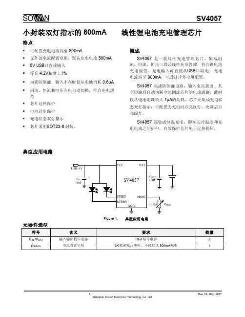
●描述SC4056H是一款高集成度、高性价比的单节锂离子电池充电器。
SC4056H采用恒定电流/恒定电压线性控制,只需较少的外部元件数目,使得SC4056H成为便携式应用的理想选择;同时,也可适合USB电源和适配器电源工作。
SC4056H采用了内部PMOSFET架构,加上防倒充电路,所以不需要外部检测电阻和隔离二极管。
热反馈可对充电电流进行自动调节,以便在大功率操作或高环境温度条件下对芯片温度加以限制。
充满电压固定于4.2V。
充电电流通过PROG脚外置电阻调节,最高可达1.2A。
当输入电压被拿掉时,SC4056H自动进入一个低电流状态,电池漏电流在3μA以下。
SC4056H的其它特点包括充电电流监控器、输入过压保护、欠压闭锁、自动再充电和两个用于指示充电结束和输入电压接入的状态引脚。
SC4056H采用绿色环保的ESOP8封装以及最少7个外围器件可有效减小电路PCB布板空间。
SC4056H可工作于-40°C to+85°C ●特点◆最高30V输入电压及6.9V过压保护◆精度达到1%的4.2V预设充电终止电压◆具有BAT-VDD防倒灌功能◆待机电流<3μA◆支持0V电池充电◆最大1.2A线性充电电流◆涓流/恒流/恒压三段式充电◆内置反接保护◆充电电流外部可调◆充电电流智能热调节◆电池温度检测保护◆自动再充电◆充电状态指示◆符合IEC62368最新标准◆ESOP8绿色封装◆欠压闭锁●应用◆移动电话,PDAs,MP3播放器◆USB数据卡◆TWS耳机充电仓◆电池充电电路◆其它手持设备●典型应用典型应用ESOP8。
5088SS(文件编号:S&CIC1620)二合一锂电池保护IC概述5088SS产品是单节锂离子/锂聚合物可充电电池组保护的高集成度解决方案。
5088SS包括了先进的功率MOSFET,高精度的电压检测电路和延时电路。
5088SS具有过充,过放,过流,短路等所有的电池所需保护功能,并且工作时功耗非常低。
该芯片适用于一切需要锂离子或锂聚合物可充电电池长时间供电的各种信息产品的应用场合。
特点内部集成等效18mΩ左右的先进的功率MOSFET;2段放电过流保护:过放电流1、负载短路电流;充电过流保护具有0V充电功能延时时间内部设定;高精度电压检测;低静态耗电流:正常工作电流3.0uA兼容ROHS和无铅标准。
采用SOP-8封装形式塑封。
应用单芯锂离子电池组; 锂聚合物电池组。
5088SS(文件编号:S&CIC1620)二合一锂电池保护IC 极限参数电气特性参数5088SS(文件编号:S&CIC1620)二合一锂电池保护IC 功能描述5088SS是一款高精度的锂电池保护电路。
正常状态下,如果对电池进行充电,则5088SS可能会进入过电压充电保护状态;同时,满足一定条件后,又会恢复到正常状态。
如果对电池放电,则可能会进入过电压放电保护状态或过电流放电保护状态;同时,满足一定条件后,也会恢复到正常状态。
正常状态在正常状态下,5088SS由电池供电,其VDD端电压在过电压充电保护阈值V OC和过电压放电保护阈值V OD 之间,VM端电压在充电器检测电压(V CHG)与过电流放电保护阈值(V EDI)之间,内置N-MOS管导通。
此时,既可以使用充电器对电池充电,也可以通过负载使电池放电。
过电压充电保护状态保护条件正常状态下,对电池进行充电,如果使VDD端电压升高超过过电压充电保护阈值V OC,且持续时间超过过电压充电保护延迟时间t OC,则5088SS将使内置N-MOS管关闭,充电回路被“切断”,即5088SS进入过电压充电保护状态。
CPC405X应用设计指南1 CPC405X概述CPC405X是一款专为低功耗系统设计的单节锂电池充电管理芯片,根据型号不同,分别带有1~2路脉冲控制可调输出电压的低功耗LDO和一路固定输出LDO,待机时功耗低至2uA。
芯片拥有1路固定输出3.3V,其它LDO输出可通过脉冲控制,输出从0.9V到3.3V。
锂电池线性充电电流可以通过外部电阻实现40mA~600mA调节。
CPC405X型号如下表:Device Enable Signal LDOsCPC4050 None 1CPC4051EN12CPC4052ENLP,EN12CPC4053 ENLP,EN1,EN2 31.1 CPC405X封装引脚图图 1CPC4050 TSOT23-6L Pin Assignment(Top View)图2 CPC4051 DFN 1.5*1.5 8L Pin Assignment(Top View)Subject: 应用文档AN40-005 V1.2 20180129 Model Name: CPC405X应用设计指南图3 CPC4052 DFN2*2 8L Pin Assignment (Top View )123VBUS LDO_LP LDO1BAT ENLP I S E T11G N DS T ALDO2E N 25N CE N 1图4 CPC4053 QFN 2*2 12L Pin Assignment (Top View )1.2 引脚定义CPC4050Name I/O DescriptionISET I Charge Current Program GND G Ground LDO_LP O 3.3V output BAT P Li-ion battery VBUS P PowerSTAOOpen-Drain Charge Status Output, pull down when chargingCPC4051Name I/O DescriptionISET I Charge Current ProgramEN1I Configuration pin of LDO1GND G GroundLDO_LP O 3.3V outputLDO1O0.9~3.3V outputBAT P Li-ion batteryVBUS P PowerSTA O Open-Drain Charge Status Output, pull down when chargingCPC4052Name I/O DescriptionISET I Charge Current ProgramENLP I Enable pin of LDO_LPEN1I Configuration pin of LDO1GND G GroundLDO_LP O 3.3V outputLDO1O0.9~3.3V outputBAT P Li-ion batteryVBUS P PowerSTA O Open-Drain Charge Status Output, pull down when chargingCPC4053Name I/O DescriptionISET I Charge Current ProgramENLP I Enable pin of LDO_LPEN1I Configuration pin of LDO1EN2I Configuration pin of LDO2GND G GroundLDO_LP O 3.3V outputLDO1O0.9~3.3V outputLDO2O0.9~3.3V outputBAT P Li-ion batteryVBUS P PowerSTA O Open-Drain Charge Status Output, pull down when charging2 CPC405X参考设计2.1 CPC405X 评估板原理图Approv al:图5 CPC405X 评估板原理图原理图中用MCU 产生的一线脉冲控制CPC405X 的LDO1和LDO2的输出电压,EN_SEL 接高,EN1有效,对应LED3亮;EN_SEL 接低,EN2有效,对应LED4亮。
�最大结温:145℃�工作环境温度范围:-40℃~85℃�贮存温度范围:-65℃~125℃�引脚温度(焊接时间10秒):260℃�高达1000mA 的充电电流�无需MOSFET 、检测电阻或隔离二极管�用于单节锂离子电池、采用SOP 封装的完整线性充电器�恒定电流/恒定电压操作,并具有可在无过热危险的情况下实现充电速率最大化的热调节功能�精度达到±1%的4.2V 预设充电电压�用于电池电量检测的充电电流监控器输出�自动再充电�充电状态双输出、无电池和故障状态显示�C/10充电终止�待机模式下的供电电流为55uA � 2.9V 涓流充电�软启动限制了浪涌电流�电池温度监测功能�采用8引脚SOP/MSOP 封装�移动电话�MP3、MP4播放器�数码相机�电子词典�GPS�便携式设备、各种充电器SS4056是一款完整的单节锂离子电池采用恒定电流/恒定电压线性充电器。
其底部带有散热片的SOP8/MSOP 封装与较少的外部元件数目使得SS4056成为便携式应用的理想选择。
SS4056可以适合USB 电源和适配器电源工作。
由于采用了内部PMOSFET 架构,加上防倒充电路,所以不需要外部隔离二极管。
热反馈可对充电电流进行自动调节,以便在大功率操作或高环境温度条件下对芯片温度加以限制。
充电电压固定于4.2V ,而充电电流可通过一个电阻器进行外部设置。
当充电电流在达到最终浮充电压之后降至设定值1/10时,SS4056将自动终止充电循环。
当输入电压(交流适配器或USB 电源)被拿掉时,SS4056自动进入一个低电流状态,将电池漏电流降至2uA 以下。
SS4056在有电源时也可置于停机模式,以而将供电电流降至55uA 。
SS4056的其他特点包括电池温度检测、欠压闭锁、自动再充电和两个用于指示充电、结束的LED 状态引脚。
�输入电源电压(Vcc ):-0.3V~8V �PROG :-0.3V~Vcc+0.3V �BAT :-0.3V~7V �CHRG :-0.3V~10V �STDBY :-0.3V~10V �TEMP :-0.3V~10V �CE :-0.3V~10V �BAT 短路持续时间:连续�BAT 引脚电流:1200mA �PROG 引脚电流:1200uA1A 线性锂离子电池充电器绝对最大额定值应用特点描述图1图2芯片的高效散热是保证芯片长时间维持较大充电电流的前提。
是一款支持双节串联锂离子电池的升压充电管理芯片,具有完善的充电保护功能。
针对不同的应用场合,芯片可以通过方便地调节外部电阻的阻值来改变充电电流的大小。
针对不同种类的适配器,芯片内置自适应电流调节环路,智能调节充电电流大小,从而防止充电电流过大而拉挂适配器的现象。
该芯片将功率管内置从而实现较少的外围器件并节约系统成本。
FS4059A 的升压开关充电转换器的工作频率为600KHz ,最大2A 输入充电,转换效率为91%。
FS4059A 输入电压为5V,内置自适应环路,可智能调节充电电流,防止拉挂适配器输出可匹配所有适配器。
FS4059A 提供ESOP8封装(底部焊盘)。
升压充电效率最高91% 充电电流外部可调自动调节输入电流,匹配所有适配器 支持LED 充电状态指示 内置功率MOS 600KHz 开关频率输出过压,输出短路保护 输入欠压,输入过压保护 过温保护 概要特性应用领域880MA充电典型电路应用图FS4059A FS4059A 内部集成功率MOS管。
小家电智能音箱移动电源/PD电子烟●●●●充电器●●●●●●●●●●●5V2A 10W输入高效开关充电,充电1A电流 便携设备●●ESD 4KV 5V 输入升压双节锂电池充电管理芯片可定制白板◼ 电源走线要尽可能宽,需单独从电源走线为IC 供电; ◼ BOOST 模块主要的电路回路走线应该短而且粗; ◼ LX 走线要短,以减少EMI ;◼ 电感和肖特基应该直接相连,连接线短而且粗,避免过孔跳线; ◼ 电源端的电容应尽可能靠近IC 放置; ◼ IC 的底部散热片是功率地,应于大片的地相连,底部散热片一定要与地可靠焊接; ◼IC 放置的地方,需要有散热设计,IC 底部散热片与PCB 板的散热区域相连,并通过多打孔和地相连; ◼ 电感,肖特基和IC ,IC 正常工作情况下,是主要发热源,可尽量做好散热处理。
PCB LAYOUT 注意事项引脚定义EPADPOWERFS4059A ESOP8◼TYPE-C输入,输入端必须增加25V-47UF的电解电容或钽电容。