Microchip推出同步升压稳压器
- 格式:docx
- 大小:10.60 KB
- 文档页数:2

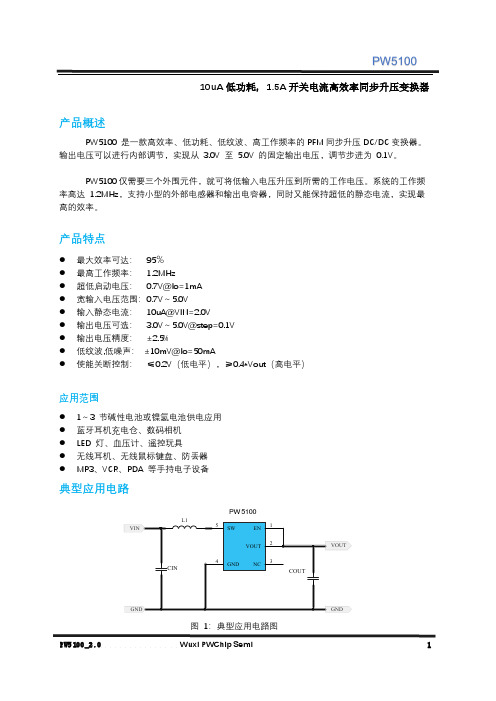
PW510010uA低功耗,1.5A开关电流高效率同步升压变换器产品概述PW5100 是一款高效率、低功耗、低纹波、高工作频率的PFM同步升压DC/DC变换器。
输出电压可以进行内部调节,实现从3.0V 至5.0V 的固定输出电压,调节步进为0.1V。
PW5100仅需要三个外围元件,就可将低输入电压升压到所需的工作电压。
系统的工作频率高达1.2MHz,支持小型的外部电感器和输出电容器,同时又能保持超低的静态电流,实现最高的效率。
产品特点⚫最大效率可达:95%⚫最高工作频率: 1.2MHz⚫超低启动电压:0.7V@Io=1mA⚫宽输入电压范围:0.7V~5.0V⚫输入静态电流:10uA@VIN=2.0V⚫输出电压可选: 3.0V~5.0V@step=0.1V⚫输出电压精度:±2.5%⚫低纹波,低噪声:±10mV@Io=50mA⚫使能关断控制:≤0.2V(低电平),≥0.4*Vout(高电平)应用范围⚫1~3 节碱性电池或镍氢电池供电应用⚫蓝牙耳机充电仓、数码相机⚫LED 灯、血压计、遥控玩具⚫无线耳机、无线鼠标键盘、防丢器⚫MP3、VCR、PDA 等手持电子设备典型应用电路PW5100图1:典型应用电路图锂电池的充电芯片电路 输入4.5V-20V 锂电池的保护板电路 集成 和DW01+8205A6S 锂电池的升压5V-15V 电路 同步和异步锂电池的降压3V-1V 电路 电流最大到3A 锂电池的升降压3.3V 电路 外围简单,输出150MA锂电池的LDO 3V,2.8V,2.5V,2V,1.8V,1.5V,1.2V 电路 三极管封装绝对最大额定值内部框图SW GNDEN电气特性(CIN =10uF,COUT =22uF,L1 =3.3uH,TA =25)特性曲线应用指南PW5100 是一款低静态电流、高效率、PFM 模式控制的同步升压变换器。
PW5100所需的外部元件非常少,只需要一个电感和输入、输出电容就可以提供 3.0V~5.0V 的稳定的低噪声输出电压。

STM32F103VET6和ENC28J60的嵌入式以太网接口设计张庆辉;马延立【摘要】介绍了一种基于STM32F103VET6微处理器和以太网控制芯片ENC28J60的嵌入式以太网接口的设计方案.分析了基于Cortex-M3内核的微处理器STM32F103VET6的功能和特点,以及以太网控制芯片ENC28J60的主要性能和结构特性,并给出了接口的硬件和软件设计方案.本接口尺寸小、性能高,适合于便携式仪器仪表中的应用.%An embedded Ethernet interface is designed based on STM32F103VET6 microprocessor and Ethernet controller chip ENC28J60. The functions and features of microprocessor STM32F103VET6 based on Cortex-M3 core are analyzed,and main performances and structural properties of Ethernet controller chip ENC28J60 are described. Hardware and software design of the interface are given. The interface has small size and high performance, and it is used for portable instruments.【期刊名称】《单片机与嵌入式系统应用》【年(卷),期】2012(012)009【总页数】4页(P23-25,32)【关键词】STM32F103VET6;ENC28J60;嵌入式以太网【作者】张庆辉;马延立【作者单位】河南工业大学信息科学与工程学院,郑州450001【正文语种】中文【中图分类】TP393.11引言随着以太网技术的普及和发展,基于以太网的应用接口设备也迅速普及到医疗设备、工厂电力系统等领域。

microchip公司的HV96001是离线LED驱动器解决方案,可以进行线性调光和PWM调光,PWM调光具有无闪烁调光,低至0.01%或更低.器件可调整AC/DC转换器输出电压,以维持大范围LED负载电压时的高转换效率.它还能对LED电流幅度进行精密控制,从而维持恒定的色温.HV96001包括两个反馈稳压器,它用来控制反馈输出电压的控制,而升压稳压器用来控制LED电流的幅度.光偶驱动器电路驱动光偶合器,依次提供控制信号,用来驱动反馈转换器的控制输入.HV96001输入电压从8V到60V,PWM调光宽度低于150ns,调光频率高达20kHz.16L VQFN 3 mm x 3 mm和16L SOIC窄体封装,主要用在离线LED照明应用.本文介绍了HV96001主要特性,框图,典型应用电路图以及离线LED驱动器评估板ADM01030主要特性,电路图,材料清单和PCB设计图.The HV96001 LED driver targets offline lighting applications requiring wide dimming capability. The device is capable of linear dimming andPWM dimming, with the PWM dimming capable of flicker-free dimmingdown to 0.01% level and lower.The HV96001 is specifically adapted to LED driver designs thataccommodate a wide range of the LED load voltage. The device adjusts the output voltage of the AC to DC conversion stage for maintaining a highconversion efficiency over a wide range of the LED load voltage. It alsomaintains a precise control over the LED current amplitude, therebymaintaining the consistent color temperature.The adaptability of the device to wide range PWM dimming allows for a stable control of the LED current waveform for PWM dimming pulse widths down to 150 ns and lower.The HV96001 driver IC adjusts the flybackconverter output voltage such that the boost converter (BC) operates with a small difference between the boost converter input and output voltage, also referred to as the headroom voltage. Operating the boost converter with a small headroom voltage, or, more or less equivalent, operating with a small voltage step-up ratio allows the boost converter to be physicallysmall and operate at a higher efficiency.The HV96001 includes two feedback regulators, the flyback regulator for control of the flyback output voltage and the boost regulator forcontrol of the LED current amplitude. An optocoupler driver circuit drives the optocoupler, which in turn provides a control signal for driving thecontrol input of the flyback converter.HV96001主要特性:• Wide Input Voltage Range: 8V to 60V• Linear (analog) Dimming:- With wide range of amplitude control of the LED current• Pulse-Width Modulation (PWM) (digital) Dimming:Microchip HV96001离线LED驱动器解决方案- Dims down to 0.01% and lower- With PWM pulse width lower than 150 ns - PWM dimming frequency up to 20 kHz • Flyback Converter:- With automatic output voltage adjustment for maintaining high system efficiency • Boost Converter:- With near zero output voltage ripple for a ripple-free LED current - 100 Hz/120 Hz ripple rejection- 200 kHz fixed switching frequency - SEPIC topology compatible • VDD Regulator:- 60V input voltage/5V output voltage - 10 mA drive for supplying external loads• Fault Recovery with Auto-Retry Delay Set Using Timing Capacitor • Undervoltage Detection of:- VDD voltage- Supply voltage (Flyback output voltage)• Overvoltage Detection of:- LED load voltage (Boost output voltage)• Overcurrent Detection of:- Load switch current• Stuck-at-Zero Detection of:- DIM input signal• Short Circuit Protection of Output with Auto-Retry DelayHV96001应用:• Offline LED lighting applications featuring wide range for PWM dimming and linear dimming.PACKAGES• 16L VQFN, 3 mm x 3 mm • 16L SOIC, Narrow Body图1.HV96001框图图2:HV96001典型应用电路图HV96001离线LED驱动器评估板ADM01030The HV96001 Offline LED Driver Evaluation Board Kit includes:• HV96001 Offline LED Driver Evaluation Board (ADM01030)• Important Information SheetHV96001 Offline LED Driver Evaluation Board is fully assembled and tested to evaluate and demonstrate the HV96001 LED driver.In the primary side, the flyback converter has implemented an activePower Factor Correction (PFC) control algorithm by a PIC controller thatcommands the switching sequence in such a manner that the input current follows the input voltage envelope. Therefore, the power factor of theapplication is PF > 0.9, for the entire input voltage range. The power factor value (PF) should be tuned by using R52 potentiometer according to the rated power of the LED load used. The tuning should be done in nodimming conditions. For example, to obtain a power factor PF over 0.9 for a 42W LED load, the value for the R52 resistor will be set to 750Ω. Check if mechanical jumper JP1 (provided) is mounted on the J11 connector.The output voltage and current delivered by the HV96001 Offline LED Driver Evaluation Board can be set by using the rotary encoder E1. Afterthe board is supplied with 230VAC the initial PWM dimming value is 50% and current reference limit LCR is 200 mV. To increase the PWM duty cycle the encoder must be rotated to the right (clockwise) and to decrease the encoder must be rotated to the left (counter-clockwise). The actual value of the PWM percent reference will be displayed on the LCD from thesecondary side of the flyback, in the first information row, as in the picture below. The value of 0.15% is given by the minimum voltage over the UVLO protection performed by the HV96001 for the input voltage. When thePWM is getting lower than 15%, the LCR is decreasing linearly to avoid big currents spikes.The maximum value of the PWM dimming is 100% and of the current reference (LCR)is 400 mV. The maximum LCR value of 400 mV iscorresponding to a 0.7-0.8A current through the LED Load.图3.离线LED驱动器评估板ADM01030外形图。

同步升压方案概述同步升压方案是一种电路设计方案,用于将输入电压转换为更高的输出电压。
这种方案通常适用于需要较高输出电压的应用,如电源模块、照明设备等。
原理同步升压方案基于电感和开关管等元件的工作原理,通过控制开关管的导通和断开来改变电感中的电流,从而实现电压的升高。
原理图原理图如图所示,同步升压方案主要包括输入电压源、电感、开关管(如MOSFET)和输出电压负载。
当开关管导通时,电感储存能量,此时输出电压为输入电压减去电压降。
当开关管断开时,电感释放储存的能量,将电流维持在一个较高的稳定水平,从而实现输出电压的升高。
优势同步升压方案相比于其他升压方案具有以下优势:1.高效性:同步升压方案利用电感及开关管的工作原理,能够更高效地转换能量,减少能量的损耗。
2.稳定性:通过合理设计电感和开关管的参数,可以使输出电压维持在一个较稳定的水平,降低因电压波动引起的不稳定情况。
3.可调节性:同步升压方案可通过控制开关管的导通和断开来改变输出电压大小,满足不同应用对于输出电压的需求。
4.抗干扰性:同步升压方案在设计时可采取一系列抗干扰措施,提高电路的抗干扰能力,使其在复杂电磁环境下能够正常工作。
实施步骤实施同步升压方案的具体步骤如下:1.确定需求:根据应用需要确定所需的输出电压范围、输出电流要求等参数。
2.选择元件:根据需求,在市场上选择合适的电感、开关管等元件,确保其工作参数符合设计要求。
3.电路设计:根据所选元件的参数,设计同步升压电路的基本结构,包括输入电压源、电感、开关管及输出负载等。
4.参数计算:计算电感值、开关频率等参数,保证电路在工作时能够满足输出要求。
5.原理验证:通过仿真软件或实际搭建电路进行原理验证,检查电路各部分的性能是否符合预期。
6.优化调整:对电路进行优化调整,如改变电感值、开关频率等参数,以获得更好的性能和稳定性。
7.PCB设计:将电路设计图转换为PCB布局图,考虑布线、电源和地线的走向,并与其他电路板进行联调。
Microchip 推出同步升压稳压器
Microchip 推出同步升压稳压器,延长电池应用寿命
Microchip Technology Inc.(美国微芯科技公司)今天宣布推出MCP1640 同步升压稳压器,它具有低至0.35V 的工作电压,静态电流低至19 微安,关断电流不到1 微安。
500 kHz 的MCP1640 稳压器具备两个集成的FET 晶体管,输出电流高达350 毫安,使消费电子市场中的电池供电应用(如电动剃须刀、牙刷、GPS 设备和便携式音乐播放器)尺寸更加小巧,电池寿命更长。
MCP1640 稳压器的工作电压低至0.35V,启动电压为0.65V,即使是
电力耗尽的单节碱性、镍氢或镍镉电池也能将其启动运行。
PWM/PFM 选项
可实现器件的低静态电流和关断电流,并实现高达96%的效率,延长了电池
的使用时间。
该稳压器的两个集成式FET 晶体管减少了元件数量,使整体设
计更为小巧。
Microchip 模拟和接口产品部副总裁Bryan Liddiard 表示:“MCP1640满足了用户在应用中减少所需电池数量的需要,同时延长了电池使用时间并
使设计更为紧凑。
”
Microchip 模拟和接口产品部高级产品营销工程师Mikhail Voroniouk 补充道:“MCP1640升压稳压器秉承了Microchip 在低功耗产品方面的优势,进一步补充了我们的超低功耗PIC®单片机产品线,尤其是必须使用单节
电池供电的应用。
”。