MP1484互换的同步降压型DC-DC稳压器MXT2484
- 格式:pdf
- 大小:1.04 MB
- 文档页数:9
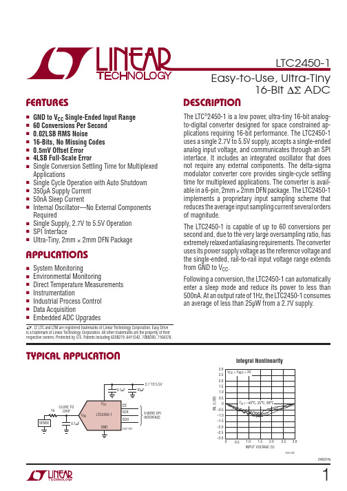
124501fbFEATURESAPPLICATIONSDESCRIPTION16-Bit ΔΣ ADCThe L TC ®2450-1 is a low power , ultra-tiny 16-bit analog-to-digital converter designed for space constrained ap-plications requiring 16-bit performance. The L TC2450-1 uses a single 2.7V to 5.5V supply, accepts a single-ended analog input voltage, and communicates through an SPI interface. It includes an integrated oscillator that does not require any external components. The delta-sigma modulator converter core provides single-cycle settling time for multiplexed applications. The converter is avail-able in a 6-pin, 2mm × 2mm DFN package. The L TC2450-1 implements a proprietary input sampling scheme that reduces the average input sampling current several orders of magnitude.The L TC2450-1 is capable of up to 60 conversions per second and, due to the very large oversampling ratio, has extremely relaxed antialiasing requirements. The converter uses its power supply voltage as the reference voltage and the single-ended, rail-to-rail input voltage range extends from GND to V CC .Following a conversion, the L TC2450-1 can automatically enter a sleep mode and reduce its power to less than 500nA. At an output rate of 1Hz, the L TC2450-1 consumes an average of less than 25μW from a 2.7V supply.nGND to V CC Single-Ended Input Range n 60 Conversions Per Second n 0.02LSB RMS Noisen 16-Bits, No Missing Codes n 0.5mV Offset Error n 4LSB Full-Scale ErrornSingle Conversion Settling Time for Multiplexed Applicationsn Single Cycle Operation with Auto Shutdown n 350μA Supply Current n 50nA Sleep Currentn Internal Oscillator—No External Components Requiredn Single Supply, 2.7V to 5.5V Operation n SPI Interface n Ultra-Tiny, 2mm × 2mm DFN PackagenSystem Monitoring n E nvironmental Monitoringn Direct Temperature Measurements n Instrumentationn Industrial Process Control n Data Acquisitionn Embedded ADC UpgradesIntegral NonlinearityL , L T , L TC and L TM are registered trademarks of Linear Technology Corporation. Easy Drive is a trademark of Linear Technology Corporation. All other trademarks are the property of their respective owners. Protected by U.S. Patents including 6208279, 6411242, 7088280, 7164378.INPUT VOL TAGE (V)–3.0I N L (L S B )–2.0–1.001.03.00.51.0 1.52.024501 G022.53.02.0–2.5–1.5–0.50.52.51.5V CC = V REF = 3VT A = –45°C, 25°C, 90°CT YPICAL APPLICATIONLTC2450-1224501fbPIN CONFIGURATIONABSOLUTE MAXIMUM RATINGSSupply Voltage (V CC ) ...................................–0.3V to 6V Analog Input Voltage (V IN ) ............–0.3V to (V CC + 0.3V)Digital Input Voltage ......................–0.3V to (V CC + 0.3V)Digital Output Voltage ...................–0.3V to (V CC + 0.3V)Operating Temperature RangeL TC2450C-1 .............................................0°C to 70°C L TC2450I-1 ..........................................–40°C to 85°C Storage Temperature Range ...................–65°C to 150°C(Notes 1, 2)PARAMETERCONDITIONSMIN TYP MAX UNITS Resolution (No missing codes)(Note 3)l 16Bits Integral Nonlinearity (Note 4)l 210LSB Offset Error l0.52mV Offset Error Drift 0.02LSB/°C Gain Error l0.010.02% of FS Gain Error Drift 0.02LSB/°C T ransition Noise1.4μV RMSThe l denotes the specifi cations which apply over the full operating temperature range, otherwise specifi cations are at T A = 25°C. (Note 2)SYMBOL PARAMETER CONDITIONSMIN TYP MAX UNITSV IN Input Voltage Range lV CCC ININ Sampling Capacitance 0.35pFI DC_LEAK (V IN )IN DC Leakage Current V IN = GND (Note 5)V IN = V CC (Note 5)l l–10–10111010nA nA I CONVInput Sampling Current (Note 9)50nAThe l denotes the specifi cations which apply over the full operating temperature range,otherwise specifi cations are at T A = 25°C.Lead Free FinishTAPE AND REEL (MINI)TAPE AND REELPART MARKING*PACKAGE DESCRIPTIONTEMPERATURE RANGE L TC2450CDC-1#TRMPBF L TC2450CDC-1#TRPBF LCTR 6-Lead (2mm × 2mm) Plastic DFN 0°C to 70°C L TC2450IDC-1#TRMPBF L TC2450IDC-1#TRPBF LCTR 6-Lead (2mm × 2mm) Plastic DFN –40°C to 85°CTRM = 500 pieces. *Temperature grades are identifi ed by a label on the shipping container .Consult L TC Marketing for parts specifi ed with wider operating temperature ranges.Consult L TC Marketing for information on lead based fi nish parts.For more information on lead free part marking, go to: http://www.linear .com/leadfree/For more information on tape and reel specifi cations, go to: http://www.linear .com/tapeandreel/TOP VIEWDC PACKAGE6-LEAD (2mm × 2mm) PLASTIC DFNV CC V IN GND 4576321SDO SCK CST JMAX = 125°C, θJA = 102°C/WEXPOSED PAD (PIN 17) IS GND, MUST BE SOLDERED TO PCBORDER INFORMATIONELECTRICAL CHARACTERISTICSANALOG INPUTLTC2450-1324501fbNote 1: Stresses beyond those listed under Absolute Maximum Ratings may cause permanent damage to the device. Exposure to any Absolute Maximum Rating condition for extended periods may affect device reliability and lifetime.Note 2: All voltage values are with respect to GND. V CC = 2.7V to 5.5V unless otherwise specifi ed.Note 3: Guaranteed by design, not subject to test.Note 4: Integral nonlinearity is defi ned as the deviation of a code from a straight line passing through the actual endpoints of the transfer curve. The deviation is measured from the center of the quantization band. Guaranteed by design, test correlation and 3 point transfer curve measurement.SYMBOL PARAMETER CONDITIONSMIN TYP MAX UNITSV CC Supply Voltage l 2.75.5V I CCSupply Current Conversion SleepCS = GND (Note 6)CS = V CC (Note 6)ll3500.056000.5μA μAThe l denotes the specifi cations which apply over the full operating temperature range,otherwise specifi cations are at T A = 25°C. (Note 2)POWER REQUIREMENTSSYMBOL PARAMETERCONDITIONSMINTYP MAX UNITSV IH High Level Input Voltage l V CC – 0.3V V IL Low Level Input Voltage l 0.3V I IN Digital Input Current l–1010μA C IN Digital Input Capacitance 10pF V OH High Level Output Voltage I O = –800μA l V CC – 0.5VV OL Low Level Output Voltage I O = –1.6mAl 0.4V I OZHi-Z Output Leakage Currentl–1010μAThe l denotes the specifi cations which apply over the full operating temperature range,otherwise specifi cations are at T A = 25°C.The l denotes the specifi cations which apply over the full operating temperature range,otherwise specifi cations are at T A = 25°C.SYMBOL PARAMETER CONDITIONSMIN TYP MAX UNITS t CONV Conversion Time l 1416.621ms f SCK SCK Frequency Range l 2MHz t lSCK SCK Low Period l 250ns t hSCK SCK High Periodl250nst 1CS Falling Edge to SDO Low Z (Notes 7, 8)l 0100ns t 2CS Rising Edge to SDO High Z(Notes 7, 8)l 0100ns t 3CS Falling Edge to SCK Falling Edge l 100ns t KQSCK Falling Edge to SDO Valid(Note 7)l100nsNote 5: CS = V CC . A positive current is fl owing into the DUT pin.Note 6: SCK = V CC or GND. SDO is high impedance.Note 7: See Figure 3.Note 8: See Figure 4.Note 9: Input sampling current is the average input current drawn from the input sampling network while the L TC2450-1 is actively sampling the input.DIGITAL INPUTS AND DIGITAL OUTPUTSTIMING CHARACTERISTICSLTC2450-1424501fbTYPICAL PERFORMANCE CHARACTERISTICSIntegral NonlinearityIntegral NonlinearityMaximum INL vs TemperatureOffset Error vs TemperatureGain Error vs TemperatureT ransition Noise vs TemperatureT ransition Noise vs Output CodeConversion Mode Power Supply Current vs TemperatureINPUT VOL TAGE (V)0–3.0I N L (L S B )–2.0–1.001.03.0 1.5 2.5 3.524501 G014.50.5 1.0 2.0 3.0 4.05.02.0–2.5–1.5–0.50.52.5 1.5V CC = V REF = 5VT A = –45°C, 25°C, 90°CINPUT VOL TAGE (V)–3.0I N L (L S B )–2.0–1.001.03.00.51.0 1.52.024501 G022.53.02.0–2.5–1.5–0.50.52.51.5V CC = V REF = 3VT A = –45°C, 25°C, 90°CTEMPERATURE (°C)–5076543210257524501 G04–2550100O F F S E T (L S B )TEMPERATURE (°C)–50–1G A I N E R R O R (L S B )1235–25025******* G05751004V CC = 4.1VV CC = 2.7VV CC = 5.5VTEMPERATURE (°C)–50 T R A N S I T I O N N O I S ER M S (μV )1.503.0010709024501 G061.000.250.500.752.502.001.252.7502.251.75–30–103050OUTPUT CODE (NORMALIZED TO FULL SCALE)0 T R A N S I T I O NN O I S E R M S (μV )1.503.000.80 1.0024501 G071.000.250.500.752.502.001.252.7502.251.750.200.400.60TEMPERATURE (°C)–45–250C O N V E R S I O N C U R R E N T (μA )200500–5355524501 G08100400300157595LTC2450-1524501fbSleep Mode Power Supply Current vs TemperatureTYPICAL PERFORMANCE CHARACTERISTICSConversion Period vs TemperatureAverage Supply Power vs Temperature, V CC = 3VTEMPERATURE (°C)–45–250S L E E P M O D E C U R R E N T (n A )100250–5355524501 G0950200150157595TEMPERATURE (°C)–45192022155524501 G111817–25–5357595161521C O N V E R S I O N T I M E(m s )TEMPERATURE (°C)–5010A V E R A G E S U P P L Y P O W E R (μW )100100010000–250255024501 G1075100LTC2450-1624501fbPIN FUNCTIONSV CC (Pin 1): Positive Supply Voltage and Converter Refer-ence Voltage. Bypass to GND (Pin 3) with a 10μF capacitor in parallel with a low series inductance 0.1μF capacitor located as close to the part as possible.V IN (Pin 2): Analog Input Voltage.GND (Pin 3): Ground. Connect to a ground plane through a low impedance connection.CS (Pin 4): Chip Select (Active LOW) Digital Input. A LOW on this pin enables the SDO digital output. A HIGH on this pin places the SDO output pin in a high imped-ance state.SDO (Pin 5): Three-State Serial Data Output. SDO is used for serial data output during the DATA OUTPUT state and can be used to monitor the conversion status.SCK (Pin 6): Serial Clock Input. SCK synchronizes the serial data output. While digital data is available (the ADC is not in CONVERT state) and CS is LOW (ADC is not in SLEEP state) a new data bit is produced at the SDO output pin following every falling edge applied to the SCK pin.Exposed Pad (Pin 7): Ground. The Exposed Pad must be soldered to the same point as Pin 3.Figure 1. Functional Block DiagramV V 24501 BDFUNCTIONAL BLOCK DIAGRAMLTC2450-1724501fbCONVERTER OPERATIONConverter Operation Cycle The L TC2450-1 is a low power , delta-sigma analog-to-digital converter with a simple 3-wire interface (see Figure 1). Its operation is composed of three successive states: CONVERT , SLEEP and DATA OUTPUT . The operat-ing cycle begins with the CONVE RT state, is followed by the SLE E P state, and ends with the DATA OUTPUT state (see Figure 2). The 3-wire interface consists of serial data output (SDO), serial clock input (SCK), and the active low chip select input (CS ). The CONVE RT state duration is determined by the L TC2450-1 conversion time (nominally 16.6 milliseconds). Once started, this operation can not be aborted except by a low power supply condition (V CC < 2.1V) which generates an internal power-on reset signal.After the completion of a conversion, the L TC2450-1enters the SLEEP state and remains there until both the chip select and clock inputs are low (CS = SCK = LOW). Following this condition the ADC transitions into the DATA OUTPUT state.Figure 2. L TC2450-1 State T ransition DiagramAPPLICATIONS INFORMATIONWhile in the SLEEP state, whenever the chip select in-put is pulled high (CS = HIGH), the L TC2450-1’s powersupply current is reduced to less than 500nA. When the chip select input is pulled low (CS = LOW), and SCK is maintained at a HIGH logic level, the L TC2450-1 will return to a normal power consumption level. During the SLEEPstate, the result of the last conversion is held indefinitely in a static register .Upon entering the DATA OUTPUT state, SDO outputs the most signifi cant bit (D15) of the conversion result. During this state, the ADC shifts the conversion result serially through the SDO output pin under the control of the SCK input pin. There is no latency in generating this data and the result corresponds to the last completed conversion. A new bit of data appears at the SDO pin following each falling edge detected at the SCK input pin. The user canreliably latch this data on every rising edge of the external serial clock signal driving the SCK pin (see Figure 3).The DATA OUTPUT state concludes in one of two different ways. First, the DATA OUTPUT state operation is completed once all 16 data bits have been shifted out and the clockthen goes low. This corresponds to the 16th falling edge of SCK. Second, the DATA OUTPUT state can be abortedat any time by a LOW-to-HIGH transition on the CS input. Following either one of these two actions, the L TC2450-1will enter the CONVERT state and initiate a new conver-sion cycle.Power-Up SequenceWhen the power supply voltage V CC applied to the con-verter is below approximately 2.1V , the ADC performs apower-on reset. This feature guarantees the integrity of the conversion result.When V CC rises above this critical threshold, the converter generates an internal power-on reset (POR) signal for approximately 0.5ms. The POR signal clears all internal registers. Following the POR signal, the L TC2450-1 starts a conversion cycle and follows the succession of states described in Figure 2. The fi rst conversion result fol-lowing POR is accurate within the specifi cations of the device if the power supply voltage V CC is restored within the operating range (2.7V to 5.5V) before the end of the POR time interval.LTC2450-1824501fbAPPLICATIONS INFORMATIONInput Voltage RangeThe ADC is capable of digitizing true rail-to-rail input sig-nals. Ignoring offset and full-scale errors, the converter will theoretically output an “all zero” digital result when the input is at ground (a zero scale input) and an “all one” digital result when the input is at V CC (a full-scale input). In an under-range condition, for all input voltages less than the voltage corresponding to output code 0, the converter will generate the output code 0. In an over-range condition, for all input voltages greater than the voltage corresponding to output code 65535 the converter will generate the output code 65535.Output Data FormatThe L TC2450-1 generates a 16-bit direct binary encoded result. It is provided, MSB fi rst, as a 16-bit serial stream through the SDO output pin under the control of the SCK input pin (see Figure 3).During the data output operation the CS input pin must be pulled low (CS = LOW). The data output process starts with the most signifi cant bit of the result being present at the SDO output pin (SDO = D15) once CS goes low. A new data bit appears at the SDO output pin following every falling edge detected at the SCK input pin. The output data can be reliably latched by the user using the rising edge of SCK.Ease of UseThe L TC2450-1 data output has no latency, fi lter settling delay or redundant results associated with the conversion cycle. There is a one-to-one correspondence between the conversion and the output data. Therefore, multiplexing multiple analog input voltages requires no special ac-tions.The L TC2450-1 includes a proprietary input sampling scheme that reduces the average input current several orders of magnitude as compared to traditional delta sigma architectures. This allows external fi lter networks to interface directly to the L TC2450-1. Since the average input sampling current is 50nA, an external RC lowpass fi lter using a 1k Ω and 0.1μF results in <1LSB error .Reference Voltage RangeThe converter uses the power supply voltage (V CC ) as the positive reference voltage (see Figure 1). Thus, the refer-ence range is the same as the power supply range, which extends from 2.7V to 5.5V . The L TC2450-1’s internal noise level is extremely low so the output peak-to-peak noise remains well below 1LSB for any reference voltage within this range. Thus the converter resolution remains at 1LSB independent of the reference voltage. INL, offset, and full-scale errors vary with the reference voltage as indicated by the Typical Performance Characteristics graphs. These error terms will decrease with an increase in the reference voltage (as the LSB size in μV increases).Figure 3. Data Output TimingKQlSCKhSCKLTC2450-1924501fbConversion Status MonitorFor certain applications, the user may wish to monitor the L TC2450-1 conversion status. This can be achieved by holding SCK HIGH during the conversion cycle. In this condition, whenever the CS input pin is pulled low (CS = LOW), the SDO output pin will provide an indication of the conversion status. SDO = HIGH is an indication of a conversion cycle in progress while SDO = LOW is an indication of a completed conversion cycle. An example of such a sequence is shown in Figure 4.Conversion s tatus m onitoring, w hile p ossible, i s n ot r equired for L TC2450-1 as its conversion time is fi xed and equal at approximately 16.6ms (21ms maximum). Therefore, ex-ternal timing can be used to determine the completion of a conversion cycle. SERIAL INTERFACEThe L TC2450-1 transmits the conversion result and receives the start of conversion command through a synchronous 3-wire interface. This interface can be used during the CONVE RT and SLE E P states to assess the conversion status and during the DATA OUTPUT state to read the conversion result, and to trigger a new conversion.APPLICATIONS INFORMATIONSerial Interface Operation ModesThe following are a few of the more common interface operation examples. Many more valid control and serial data output operation sequences can be constructed based upon the above description of the function of the three digital interface pins.The modes of operation can be summarized as follows:1) The L TC2450-1 functions with SCK idle high (commonly known as CPOL = 1) or idle low (commonly known as CPOL = 0).2) After the 16th bit is read, the user can choose one of two ways to begin a new conversion. First, one can pull CS high (CS = ↑). Second, one can use a high-low transition on SCK (SCK = ↓).3) At any time during the Data Output state, pulling CS high (CS = ↑) causes the part to leave the I/O state, abort the output and begin a new conversion.4) When SCK = HIGH, it is possible to monitor the conver-sion status by pulling CS low and watching for SDO to go low. This feature is available only in the idle-high (CPOL = 1) mode.Figure 4. Conversion Status Monitoring ModeSDOSCK = HICSLTC2450-11024501fbAPPLICATIONS INFORMATIONSerial Clock Idle-High (CPOL = 1) ExamplesIn Figure 5, following a conversion cycle the L TC2450-1 automatically enters the low power sleep mode. The user can monitor the conversion status at convenient intervals using CS and SDO.CS is pulled LOW while SCK is HIGH to test whether or not the chip is in the CONVERT state. While in the CONVERT state, SDO is HIGH while CS is LOW . In the SLEEP state, SDO is LOW while CS is LOW . These tests are not required operational steps but may be useful for some applications.When the data is available, the user applies 16 clock cycles to transfer the result. The CS rising edge is then used to initiate a new conversion.The operation example of Figure 6 is identical to that of Figure 5, except the new conversion cycle is triggered bythe falling edge of the serial clock (SCK). A 17th clock pulse is used to trigger a new conversion cycle.Serial Clock Idle-Low (CPOL = 0) ExamplesIn Figure 7, following a conversion cycle the L TC2450-1 automatically enters the low power sleep state. The user determines data availability (and the end of conversion) based upon external timing. The user then pulls CS low (CS = ↓) and uses 16 clock cycles to transfer the result. Following the 16th rising edge of the clock, CS is pulled high (CS = ↑), which triggers a new conversion.The timing diagram in Figure 8 is identical to that of Figure 7, except in this case a new conversion is triggered by SCK. The 16th SCK falling edge triggers a new conversion cycle and the CS signal is subsequently pulled high.Figure 5. Idle-High (CPOL = 1) Serial Clock Operation Example.The Rising Edge of CS Starts a New ConversionFigure 6. Idle-High (CPOL = 1) Clock Operation Example.A 17th Clock Pulse is Used to Trigger a New Conversion CycleLTC2450-11124501fbExamples of Aborting Cycle using CSFor some applications the user may wish to abort the I/O cycle and begin a new conversion. If the L TC2450-1 is in the data output state, a CS rising edge clears the remaining data bits from memory, aborts the output cycle and triggers a new conversion. Figure 9 shows an example of aborting an I/O with idle-high (CPOL = 1) and Figure 10 shows an example of aborting an I/O with idle-low (CPOL = 0).A new conversion cycle can be triggered using the CS signal without having to generate any serial clock pulses as shown in Figure 11. If SCK is maintained at a LOW logic level, after the end of a conversion cycle, a newconversion operation can be triggered by pulling CS low and then high. When CS is pulled low (CS = LOW), SDO will output the most signifi cant bit (D15) of the result of the just completed conversion. While a low logic level is maintained at SCK pin and CS is subsequently pulled high (CS = HIGH) the remaining 15 bits of the result (D14:D0) are discarded and a new conversion cycle starts.Following the aborted I/O, additional clock pulses in the CONVERT state are acceptable, but excessive signal tran-sitions on SCK can potentially create noise on the ADC during the conversion, and thus may negatively infl uence the conversion accuracy.APPLICATIONS INFORMATIONFigure 8. Idle-Low (CPOL = 0) Clock. The 16th SCK Falling Edge T riggers a New ConversionFigure 7. Idle-Low (CPOL = 0) Clock. C S T riggers a New ConversionLTC2450-1APPLICATIONS INFORMATIONFigure 9. Idle-High (CPOL = 1) Clock and Aborted I/O ExampleFigure 10. Idle-Low (CPOL = 0) Clock and Aborted I/O ExampleFigure 11. Idle-Low (CPOL = 0) Clock and Minimum Data Output Length Example 1224501fbLTC2450-11324501fbAPPLICATIONS INFORMATIONFigure 12. 2-Wire, Idle-High (CPOL = 1) Serial Clock, Operation ExampleFigure 13. 2-Wire, Idle-Low (CPOL = 0) Serial Clock Operation Example2-Wire OperationThe 2-wire operation modes, while reducing the number of required control signals, should be used only if the L TC2450-1 low power sleep capability is not required. In addition the option to abort serial data transfers is no longer available. Hardwire CS to GND for 2-wire operation.Figure 12 shows a 2-wire operation sequence which uses an idle-high (CPOL = 1) serial clock signal. The conversion status can be monitored at the SDO output. Following a conversion cycle, the ADC enters SLEEP state and the SDO output transitions from HIGH to LOW . Subsequently 16 clock pulses are applied to the SCK input in order to serially shift the 16 bit result. Finally, the 17th clock pulse is applied to the SCK input in order to trigger a new conversion cycle.Figure 13 shows a 2-wire operation sequence which uses an idle-low (CPOL = 0) serial clock signal. The conversionstatus cannot be monitored at the SDO output. Following a conversion cycle, the L TC2450-1 bypasses the SLEEP state and immediately enters the DATA OUTPUT state. At this moment the SDO pin outputs the most signifi cant bit (D15) of the conversion result. The user must use external timing in order to determine the end of conversion and result availability. Subsequently 16 clock pulses are applied to SCK in order to serially shift the 16-bit result. The 16th clock falling edge triggers a new conversion cycle.PRESERVING THE CONVERTER ACCURACYThe L TC2450-1 is designed to reduce as much as possible the conversion result sensitivity to device decoupling, PCB layout, antialiasing circuits, line and frequency perturbations. Nevertheless, in order to preserve the very high accuracy capability of this part, some simple precautions are desirable.LTC2450-11424501fbAPPLICATIONS INFORMATIONDigital Signal LevelsThe L TC2450-1’s digital interface is easy to use. Its digital inputs (SCK and CS ) accept standard CMOS logic levels and the internal hysteresis receivers can tolerate edge rates as slow as 100μs. However , some considerations are required to take advantage of the exceptional accuracy and low supply current of this converter .The digital output signal SDO is less of a concern because it is not active during the conversion cycle.While a digital input signal is in the range 0.5V to V CC –0.5V , the CMOS input receiver may draw additional current from the power supply. Due to the nature of CMOS logic, a slow transition within this voltage range may cause an increase in the power supply current drawn by the converter , particularly in the low power operation mode within the SLEEP state. Thus, for low power consumption it is highly desirable to provide relatively fast edges for the two digital input pins SCK and CS , and to keep the digital input logic levels at V CC or GND.At the same time, during the CONVERT state, undershoot and/or overshoot of fast digital signals connected to the L TC2450-1 pins may affect the conversion result. Under-shoot and overshoot can occur because of an impedance mismatch at the converter pin combined with very fast transition times. This problem becomes particularly diffi cult when shared control lines are used and multiple refl ec-tions may occur . The solution is to carefully terminate all transmission lines close to their characteristic impedance. Parallel termination is seldom an acceptable option in low power systems so a series resistor between 27Ω and 56Ω placed near the driver may eliminate this problem. The actual resistor value depends upon the trace impedance and connection topology. An alternate solution is to reduce the edge rate of the control signals, keeping in mind the concerns regarding slow edges mentioned above.Particular attention should be given to confi gurations in which a continuous clock signal is applied to SCK pin dur-ing the CONVERT state. While L TC2450-1 will ignore this signal from a logic point of view the signal edges may create unexpected errors depending upon the relation between its frequency and the internal oscillator frequency. In such a situation it is benefi cial to use edge rates of about 10nsand to limit potential undershoot to less than 0.3V belowGND and overshoot to less than 0.3V above V CC .Noisy external circuitry can potentially impact the output under 2-wire operation. In particular , it is possible to get the L TC2450-1 into an unknown state if an SCK pulse is missed or noise triggers an extra SCK pulse. In this situ-ation, it is impossible to distinguish SDO = 1 (indicating conversion in progress) from valid “1” data bits. As such, CPOL = 1 is recommended for the 2-wire mode. The user should look for SDO = 0 before reading data, and look for SDO = 1 after reading data. If SDO does not return a “0” within the maximum conversion time (or return a “1” after a full data read), generate 16 SCK pulses to force a new conversion.Driving V CC and GNDThe V CC and GND pins of the L TC2450-1 converter are directly connected to the positive and negative reference voltages, respectively. A simplifi ed equivalent circuit is shown in Figure 14.The power supply current passing through the parasitic layout resistance associated with these common pins will modify the ADC reference voltage and thus negatively affect the converter accuracy. It is thus important to keep the V CC and GND lines quiet, and to connect these supplies through very low impedance traces.In relation to the V CC and GND pins, the L TC2450-1 com-bines internal high frequency decoupling with dampingFigure 14. L TC2450-1 Analog Pins Equivalent CircuitR SW (TYP)C EQ (TYP)0.35pFINTERNAL SWITCHING FREQUENCY = 4 MHz。

DESCRIPTIONThe MXT2482SX is a monolithic synchronous buck regulator. The device integrates 150mΩMOSFETS that provide 2A continuous load current over a wide operating input voltage of 4.5 to 23V. Current mode control provides fast transient response and cycle-by-cycle current limit.An adjustable soft-start prevents inrush current at turn-on. In shutdown mode, the supply current drops below 1µA.This device, available in an 8-pin SOIC package, provides a very compact system solution with minimal reliance on external components.PACKAGE REFERENCE FEATURES. • 2-2.5A Output Current. • Wide 4.5-23V Operating Input Range. • Integrated 150mΩ Power MOSFET Switches. • Output Adjustable from from 0.925 to 20V. • Up to 95% Efficiency. • Programmable Soft-Start. • Stable with Low ESR Ceramic Output Capacitors. • Fixed 450KHz Frequency. • Cycle-by-Cycle Over Current Protection. • Input Under Voltage Lockout. • Thermally Enhanced 8-Pin SOIC/SOIC-E PackageAPPLICATIONS. • Distributed Power Systems. • Networking Systems. • FPGA, DSP, ASIC Power Supplies. • Green Electronics/ Appliances. • Notebook ComputersABSOLUTE MAXIMUM RATINGS(1)Supply Voltage (V IN ).......................-0.3V to 26VSwitch Voltage (V SW )............. –1V to V IN + 0.3V Bootstrap Voltage (V BS ) ...Vsw-0.3V to V SW+ 6V Enable/UVLO Voltage (V EN )...........–0.3V to +6VComp Voltage (V COMP ) ...................–0.3V to +6VFeedback Voltage (V FB ) ................–0.3V to +6VJunction Temperature ........................... +150°C Lead Temperature ................................. +260°CStorage Temperature.............. –55°C to +150°CRecommended Operating Conditions(2)Input Voltage (V IN ) ......................... 4.5V to 23V Output Voltage (V SW ) ....................... 0.925 to 20VOperating Temperature...............–20°C to +85°CThermal Resistance (3)θJA θJCSOIC8N (4).............................. 50...... 10... °C/WNotes:1) Exceeding these ratings may damage the device. 2) The device is not guaranteed to function outside of itsoperating conditions. 3) Measured on approximately 1” square of 1 oz copper. 4) Measured only with solder exposed pad toboardMXT2482SX MXT2482SX MXT2482SXMXT2482SXMXT2482SX MXT2482SX MXT2482SXMXT2482SXMXT2482SXAELECTRICAL CHARACTERISTICSV IN = 12V, T A = +25°C, unless otherwise noted.Parameter Condition Min Typ Max Units Shutdown Supply Current V EN ≤ 0.3V 0.3 3.0 µA Supply Current V EN ≥ 2.6V, V FB = 1.0V 1.3 1.5 mA Feedback Voltage 4.5V ≤ V IN ≤23V 900 925 950 mV Feedback Overvoltage Threshold 1.1 V Error Amplifier Voltage 480 V/V Error Amplifier Transconductance I C = 10µA 800 µA/V High-Side Switch-On Resistance 150(4) mΩLow-Side Switch-On Resistance 150(4) mΩHigh-Side Switch Leakage V EN = 0V, V SW = 0V 0.1 10 µA Upper Switch Current Limit 2.4 3.7 A Lower Switch Current Limit 0.9 A COMP to Current SenseTransconductance 4.0 А/V Oscillator Frequency 400 450 500 KHz Short Circuit Frequency V FB = 0V 160 KHz Maximum Duty Cycle V FB = 0.8V 90 % Minimum On Time 120 nS EN Shutdown Threshold Voltage V EN Rising 1.1 1.5 2.0 V EN Shutdown Threshold VoltageHysterisis 140(4) mV EN Lockout Threshold Voltage 2.2 2.5 2.7 V EN Lockout Hysterisis 140(4) mV Input UVLO Threshold Rising V IN Rising 3.80 4.10 4.40 V Input UVLO Threshold Hysteresis 210 mV Soft-start Current V SS = 0V 6.0 µA Soft-start Period C SS = 0.1µF 15 ms Thermal Shutdown4 160 CNote:4) Guaranteed by designTYPICAL APPLICATIONPIN FUNCTIONS Pin # Name Description1 BS High-Side Gate Drive Boost Input. BS supplies the drive for the high-side N-Channel MOSFET switch. Connect a 0.01µF or greater capacitor from SW to BS to power the high side switch.2 IN Power Input. IN supplies the power to the IC, as well as the step-down converter switches. Drive IN with a 4.5V to 23V power source. Bypass IN to GND with a suitably large capacitor to eliminate noise on the input to the IC. See Input Capacitor.3 SW Power Switching Output. SW is the switching node that supplies power to the output. Connect the output LC filter from SW to the output load. Note that a capacitor is required from SW to BS to power the high-side switch.4 GND Ground (Connect Exposed Pad to Pin 4).5 FB Feedback Input. FB senses the output voltage to regulate that voltage. Drive FB with a resistive voltage divider from the output voltage. The feedback threshold is 0.925V. See Setting the Output Voltage.6 COMP Compensation Node. COMP is used to compensate the regulation control loop. Connect a series RC network from COMP to GND to compensate the regulation control loop. In some cases, an additional capacitor from COMP to GND is required. See Compensation Components.7 EN Enable Input. EN is a digital input that turns the regulator on or off. Drive EN high to turn on the regulator, drive it low to turn it off. Pull up with 100kΩ resistor for automatic startup.8 SS Soft-Start Control Input. SS controls the soft-start period. Connect a capacitor from SS to GND to set the soft-start period. A 0.1µF capacitor sets the soft-start period to 15ms. To disable the soft-start feature, leave SS unconnected.MXT2482SXOPERATIONFUNCTIONAL DESCRIPTIONThe MXT2482SX is a synchronous rectified, current-mode, step-down regulator. It regulates input voltages from 4.5V to 23V down to an output voltage as low as 0.925V, and supplies upto 2A of load current. The MXT2482SX uses current-mode control to regulate the output voltage. The output voltage is measured at FB through a resistive voltage divider and amplifiedthrough the internal transconductance error amplifier. The voltage at the COMP pin is compared to the switch current measured internally to control the output voltage.The converter uses internal N-Channel MOSFET switches to step-down the input voltage tothe regulated output voltage. Since the high side MOSFET requires a gate voltage greaterthan the input voltage, a boost capacitor connected between SW and BS is needed to drivethe high side gate. The boost capacitor is charged from the internal 5V rail when SW is low. When the MXT2482SX FB pin exceeds 20% of the nominal regulation voltage of 0.925V, the over voltage comparator is tripped and the COMP pin and the SS pin are discharged to GND, forcing the high-side switch off.Figure 1 – Functional Block DiagramAPPLICATION INFORMATION COMPONENT SELECTION Settingthe Output VoltageThe output voltage is set using a resistivevoltage divider from the output voltage to FB(see Typical Application circuit on page 1). Thevoltage divider divides the output voltage downby the rat io:Where V FB is the feedback voltage and V OUT isthe output voltage.Thus the output voltage is:R2 can be as high as 100kΩ, but a typical value is 10kΩ. Using the typical value for R2, R1 is determined by:For example, for a 3.3V output voltage, R2 is 10kΩ, and R1 is 26.1kΩ. Table 1 lists recommended resistance values of R1 and R2 for standard output voltages.calculated by:Where V OUT is the output voltage, V IN is the input voltage, f S is the switching frequency, and ∆I L is the peak-to-peak inductor ripple current. Choose an inductor that will not saturate under the maximum inductor peak current. The peak inductor current can be calculated by:Where I LOAD is the load current. The choice of which style inductor to use mainly depends on the price vs. size requirements and any EMI requirements.Optional Schottky DiodeDuring the transition between high-side switch and low-side switch, the body diode of the lowside power MOSFET conducts the inductor current. The forward voltage of this body diode is high. An optional Schottky diode may be paralleled between the SW pin and GND pin to improve overall efficiency. Table 2 lists example Schottky diodes and their Manufacturers.Table 2 – Diode Selection GuideInductorThe inductor is required to supply constant current to the output load while being driven by the switched input voltage. A larger value inductor will result in less ripple current that will result in lower output ripple voltage. However, the larger value inductor will have a larger physical size, higher series resistance, and/or lower saturation current. A good rule for determining the inductance to use is to allow the peak-to-peak ripple current in the inductor to be approximately 30% of the maximum switch current limit. Also, make sure that the peak inductor current is below the maximum switch current limit. The inductance value can beVendorPart Number Voltage/CurrentRatingB130 30V, 1A Diodes, Inc.SK13 30V, 1A Diodes, Inc.MBRS130 30V, 1A InternationalRectifierInput CapacitorThe input current to the step-down converter is discontinuous, therefore a capacitor is required to supply the AC current to the step-down converter while maintaining the DC input voltage. Use low ESR capacitors for the best performance. Ceramic capacitors are preferred, but tantalum or low-ESR electrolytic capacitors may also suffice. Choose X5R or X7R dielectrics when using ceramic capacitors. Since the input capacitor absorbs the input switching current it requires an adequate ripple current rating. The RMS current in the input capacitor can be estimated by:The worst-case condition occurs at V IN = 2V OUT, where I CIN = I LOAD/2. For simplification, choose the input capacitor whose RMS current rating greater than half of the maximum load current. The input capacitor can be electrolytic, tantalum or ceramic. When using electrolytic or tantalum capacitors, a small, high quality ceramic capacitor, i.e. 0.1µF, should be placed as close to the IC as possible. When using ceramic capacitors, make sure that they have enough capacitance to provide sufficient charge to prevent excessive voltage ripple at input. The input voltage ripple for low ESR capacitors can be estimated by:Where C IN is the input capacitance value.Output CapacitorThe output capacitor is required to maintain the DC output voltage. Ceramic, tantalum, or low ESR electrolytic capacitors are recommended. Low ESR capacitors are preferred to keep the output voltage ripple low. The output voltageripple can be estimated by:Where C O is the output capacitance value and R ESR is the equivalent series resistance (ESR) value of the output capacitor. In the case of ceramic capacitors, the impedance at the switching frequency is dominated by the capacitance. The output voltage ripple is mainly caused by the capacitance. For simplification, the output voltage ripple can be estimated by:In the case of tantalum or electrolytic capacitors, the ESR dominates the impedance at the switching frequency. For simplification, the output ripple can be approximated to:The characteristics of the output capacitor also affect the stability of the regulation system. TheMXT2482SX can be optimiz ed for a wide range of capacitance and ESR values. Compensation ComponentsMXT2482SX employs current mode c o ntrol for easy compensation and fast transient response. The system stability and transient response are controlled through the COMP pin. COMP pin is the output of the internal transconductance error amplifier. A series capacitor-resistor combination sets a pole-zero combination to control the characteristics of the control system. The DC gain of the voltage feedback loop is given by:Where V FB is the feedback voltage, 0.925V; A VEA is the error amplifier voltage gain; G CS is the current sense transconductance and R LOAD is the load resistor value. The system has two poles of importance. One is due to the compensation capacitor (C3) and the output resistorof the error amplifier, and the other is due to the output capacitor and the load resistor.These poles are located at:Where G EA is the error amplifier transconductance.The system has one zero of importance, due to the compensation capacitor (C3) and thecompensation resistor (R3). This zero is located at:The system may have another zero of importance, if the output capacitor has a large capacitance and/or a high ESR value. The zero, due to the ESR and capacitance of the output capacitor, is located at:In this case (as shown in Figure 2), a third pole set by the compensation capacitor (C6) and the compensation resistor (R3) is used to compensate the effect of the ESR zero on the loop gain. This pole is located at:The goal of compensation design is to shape the converter transfer function to get a desired loop gain. The system crossover frequency where the feedback loop has the unity gain is important. Lower crossover frequencies result in slower line and load transient responses, while higher crossover frequencies could cause system instability. A good rule of thumb is to set the crossover frequency below one-tenth of the switching frequency.To optimize the compensation components, the following procedure can be used.1. Choose the compensation resistor (R3) to set the desired crossover frequency. Determine the R3 value by the following equation:Wheref C is the desired crossover frequency which is typically below one tenth of the switching frequency.2. 2. Choose the compensation capacitor (C3) to achieve the desired phase margin.For applications with typical inductor values, setting the compensation zero, f Z1, belowone-forth of the crossover frequency provides sufficient phase margin. Determine the C3 value by the following equation:R3 is the compensation resistor.3. Determine if the second compensation capacitor (C6) is required. It is required if the ESR zero of the output capacitor is located at less than half of the switching frequency, or the following relationship is valid:If this is the case, then add the second compensation capacitor (C6) to set the pole f P3 at the location of the ESR zero. Determine the C6 value by the equation:External Bootstrap DiodeAn external bootstrap diode may enhance the efficiency of the regulator, the applicable conditions of external BST diode are V OUT =5V or 3.3V. This diode is also recommended forhigh dutycycle operation (whenoutput voltage (V OUT >12V) applications.Figure 2—External Bootstrap DiodeThe recommended external BST diode is IN4148, and the BST cap is 0.1~1uFTYPICAL APPLICATION CIRCUITSFigure 3 — MXT2482SX with 3.3V Output, 22µF/6.3V Ceramic Output CapacitorMXT2482SXMXT2482SX。

常⽤替换运放型号对⽐常⽤替换运放型号对⽐CA3130 ⾼输⼊阻抗运算放⼤器 Intersil[DATA] CA3140 ⾼输⼊阻抗运算放⼤器 CD4573 四可编程运算放⼤器 MC14573ICL7650 斩波稳零放⼤器 LF347(NS[DATA]) 带宽四运算放⼤器 KA347 LF351 BI-FET单运算放⼤器 NS[DATA] LF353 BI-FET双运算放⼤器 NS[DATA] LF356 BI-FET单运算放⼤器 NS[DATA] LF357 BI-FET单运算放⼤器 NS[DATA] LF398 采样保持放⼤器 NS[DATA] LF411 BI-FET单运算放⼤器 NS[DATA] LF412 BI-FET双运放⼤器 NS[DATA] LM124 低功耗四运算放⼤器(军⽤档) NS[DATA]/TI[DATA] LM1458 双运算放⼤器 NS[DATA] LM148 四运算放⼤器 NS[DATA] LM224J 低功耗四运算放⼤器(⼯业档)NS[DATA]/TI[DATA] LM2902 四运算放⼤器 NS[DATA]/TI[DATA] LM2904 双运放⼤器 NS[DATA]/TI[DATA] LM301 运算放⼤器 NS[DATA] LM308 运算放⼤器 NS[DATA] LM308H 运算放⼤器(⾦属封装) NS[DATA] LM318 ⾼速运算放⼤器NS[DATA] LM324(NS[DATA]) 四运算放⼤器 HA17324,/LM324N(TI) LM348 四运算放⼤器 NS[DATA] LM358 NS[DATA] 通⽤型双运算放⼤器 HA17358/LM358P(TI) LM380 ⾳频功率放⼤器NS[DATA] LM386-1 NS[DATA] ⾳频放⼤器NJM386D,UTC386 LM386-3 ⾳频放⼤器 NS[DATA] LM386-4 ⾳频放⼤器 NS[DATA] LM3886 ⾳频⼤功率放⼤器 NS[DATA] LM3900 四运算放⼤器 LM725 ⾼精度运算放⼤器NS[DATA] LM733 带宽运算放⼤器 LM741 NS[DATA] 通⽤型运算放⼤器HA17741 MC34119 ⼩功率⾳频放⼤器 NE5532 ⾼速低噪声双运算放⼤器 TI[DATA] NE5534 ⾼速低噪声单运算放⼤器TI[DATA] NE592 视频放⼤器 OP07-CP 精密运算放⼤器 TI[DATA] OP07-DP 精密运算放⼤器 TI[DATA] TBA820M ⼩功率⾳频放⼤器 ST[DATA] TL061 BI-FET单运算放⼤器 TI[DATA] TL062 BI-FET双运算放⼤器 TI[DATA] TL064 BI-FET 四运算放⼤器 TI[DATA] TL072 BI-FET双运算放⼤器 TI[DATA] TL074 BI-FET四运算放⼤器 TI[DATA] TL081 BI-FET单运算放⼤器TI[DATA] TL082 BI-FET双运算放⼤器 TI[DATA] TL084 BI-FET四运算放⼤器 TI[DATA] AD824 JFET输⼊,单电源,低电压,低功耗,精密四运算放⼤器 MC33171 单电源,低电压,低功耗运算放⼤器 AD826 低功耗,宽带,⾼速双运算放⼤器 MC33172 单电源,低电压,低功耗双运算放⼤器AD827 低功耗,⾼速双运算放⼤器 MC33174 单电源,低电压,低功耗四运算放⼤器 AD828 低功耗,宽带,⾼速双运算放⼤器 MC33178 ⼤电流,低功耗,低噪⾳双运算放⼤器 AD844 电流反馈型,宽带,⾼速运算放⼤器 MC33179 ⼤电流,低功耗,低噪⾳四运算放⼤器 AD846 电流反馈型,⾼速,精密运算放⼤器 MC33181 JFET输⼊,低功耗运算放⼤器 AD847 低功耗,⾼速运算放⼤器 MC33182 JFET输⼊,低功耗双运算放⼤器AD8531 COMS单电源,低功耗,⾼速运算放⼤器 MC33184 JFET 输⼊,低功耗四运算放⼤器 AD8532 COMS单电源,低功耗,⾼速双运算放⼤器 MC33201 单电源,⼤电流,低电压运算放⼤器AD8534 COMS单电源,低功耗,⾼速四运算放⼤器 MC33202 单电源,⼤电流,低电压双运算放⼤器 AD9617 低失真,电流反馈型,宽带,⾼速,精密运算放⼤器 MC33204 单电源,⼤电流,低电压四运算放⼤器 AD9631 低失真,宽带,⾼速运算放⼤器MC33272 单电源,低电压,⾼速双运算放⼤器 AD9632 低失真,宽带,⾼速运算放⼤器 MC33274 单电源,低电压,⾼速四运算放⼤器 AN6550 低电压双运算放⼤器 MC33282 JFET输⼊,宽带,⾼速双运算放⼤器AN6567 ⼤电流,单电源双运算放⼤器 MC33284 JFET输⼊,宽带,⾼速四运算放⼤器 AN6568 ⼤电流,单电源双运算放⼤器 MC33502 BIMOS,单电源,⼤电流,低电压,双运算放⼤器 BA718 单电源,低功耗双运算放⼤器MC34071A 单电源,⾼速运算放⼤器 BA728 单电源,低功耗双运算放⼤器 MC34072A 单电源,⾼速双运算放⼤器 CA5160 BIMOS,单电源,低功耗运算放⼤器 MC34074A 单电源,⾼速四运算放⼤器 CA5260 BIMOS,单电源双运算放⼤器 MC34081 JFET输⼊,宽带,⾼速运算放⼤器 CA5420 BIMOS,单电源,低电压,低功耗运算放⼤器 MC34082 JFET输⼊,宽带,⾼速双运算放⼤器 CA5470 BIMOS单电源四运算放⼤器 MC34084 JFET输⼊,宽带,⾼速四运算放⼤器CLC400 电流反馈型,宽带,⾼速运算放⼤器 MC34181 JFET输⼊,低功耗运算放⼤器 CLC406 电流反馈型,低功耗,宽带,⾼速运算放⼤器 MC34182 JFET输⼊,低功耗双运算放⼤器 CLC410 电流反馈型,⾼速运算放⼤器 MC34184 JFET输⼊,低功耗四运算放⼤器 CLC415 电流反馈型,宽带,⾼速四运算放⼤器 MC35071A 单电源,⾼速运算放⼤器 CLC449 电流反馈型,宽带,⾼速运算放⼤器 MC35072A 单电源,⾼速双运算放⼤器 CLC450 电流反馈型,单电源,低功耗,宽带,⾼速运算放⼤器 MC35074A 单电源,⾼速四运算放⼤器 CLC452 单电源,电流反馈型,⼤电流,低功耗,宽带,⾼速运算放⼤器 MC35081 JFET输⼊,宽带,⾼速运算放⼤器CLC505 电流反馈型,⾼速运算放⼤器 MC35082 JFET输⼊,宽带,⾼速双运算放⼤器 EL2030 电流反馈型,宽带,⾼速运算放⼤器 MC35084 JFET输⼊,宽带,⾼速四运算放⼤器 EL2030C 电流反馈型,宽带,⾼速运算放⼤器 MC35171 单电源,低电压,低功耗运算放⼤器 EL2044C 单电源,低功耗,⾼速运算放⼤器 MC35172 单电源,低电压,低功耗双运算放⼤器 EL2070 电流反馈型,宽带,⾼速运算放⼤器 MC35174 单电源,低电压,低功耗四运算放⼤器 EL2070C 电流反馈型,宽带,⾼速运算放⼤器 MC35181 JFET输⼊,低功耗运算放⼤器 EL2071C 电流反馈型,宽带,⾼速运算放⼤器 MC35182 JFET输⼊,低功耗双运算放⼤器 EL2073 宽带,⾼速运算放⼤器 MC35184 JFET输⼊,低功耗四运算放⼤器 EL2073C 宽带,⾼速运算放⼤器 MM6558 低电压,低失调电压,精密双运算放⼤器 EL2130C 电流反馈型,宽带,⾼速运算放⼤器MM6559 低电压,低失调电压,精密双运算放⼤器 EL2150C 单电源,宽带,⾼速运算放⼤器 MM6560 低电压,低失调电压,精密双运算放⼤器 EL2160C电流反馈型,宽带,⾼速运算放⼤器 MM6561 低功耗,低电压,低失调电压,精密双运算放⼤器 EL2165C 电流反馈型,宽带,⾼速,精密运算放⼤器 MM6564 单电源,低电压,低功耗,低失调电压,精密双运算放⼤器 EL2170C 单电源,电流反馈型,低功耗,宽带,⾼速运算放⼤器MM6572 低噪⾳,低电压,低失调电压,精密双运算放⼤器 EL2175C 电流反馈型,宽带,⾼速,精密运算放⼤器 NE5230单电源,低电压运算放⼤器 EL2180C 单电源,电流反馈型,低功耗,宽带,⾼速运算放⼤器NE5512 通⽤双运算放⼤器 EL2224 宽带,⾼速双运算放⼤器 NE5514 通⽤四运算放⼤器 EL2224C 宽带,⾼速双运算放⼤器NE5532 低噪⾳,⾼速双运算放⼤器 EL2232 电流反馈型,宽带,⾼速双运算放⼤器NE5534 低噪⾳,⾼速运算放⼤器 EL2232C 电流反馈型,宽带,⾼速双运算放⼤器 NJM2059 通⽤四运算放⼤器 EL2250C 单电源,宽带,⾼速双运算放⼤器 NJM2082 JFET输⼊,⾼速双运算放⼤器 EL2260C 电流反馈型,宽带,⾼速双运算放⼤器 NJM2107低电压,通⽤运算放⼤器 EL2270C 单电源,电流反馈型,低功耗,宽带,⾼速双运算放⼤器 NJM2112 低电压,通⽤四运算放⼤器EL2280C 单电源,电流反馈型,低功耗,宽带,⾼速双运算放⼤器 NJM2114 低噪⾳双运算放⼤器 EL2424 宽带,⾼速四运算放⼤器NJM2115 低电压,通⽤双运算放⼤器 EL2424C 宽带,⾼速四运算放⼤器 NJM2119 单电源,精密双运算放⼤器 EL2444C 单电源,低功耗,⾼速四运算放⼤器 NJM2122 低电压,低噪⾳双运算放⼤器 EL2450C 单电源,宽带,⾼速四运算放⼤器 NJM2130F 低功耗运算放⼤器 EL2460C 电流反馈型,宽带,⾼速四运算放⼤器 NJM2132 单电源,低电压,低功耗双运算放⼤器 EL2470C 单电源,电流反馈型,低功耗,宽带,⾼速四运算放⼤器 NJM2136 低电压,低功耗,宽带,⾼速运算放⼤器 EL2480C 单电源,电流反馈型,低功耗,宽带,⾼速四运算放⼤器NJM2137 低电压,低功耗,宽带,⾼速双运算放⼤器 HA-2640 ⾼耐压运算放⼤器 NJM2138 低电压,低功耗,宽带,⾼速四运算放⼤器 HA-2645 ⾼耐压运算放⼤器 NJM2140 低电压双运算放⼤器 HA-2839 宽带,⾼速运算放⼤器NJM2141 ⼤电流,低电压双运算放⼤器 HA-2840 宽带,⾼速运算放⼤器 NJM2147 ⾼耐压,低功耗双运算放⼤器 HA-2841 宽带,⾼速运算放⼤器 NJM2162 JFET输⼊,低功耗,⾼速双运算放⼤器HA-2842 宽带,⾼速运算放⼤器 NJM2164 JFET输⼊,低功耗,⾼速四运算放⼤器 HA-4741 通⽤四运算放⼤器 NJM3404A 单电源,通⽤双运算放⼤器 HA-5020 电流反馈型,宽带,⾼速运算放⼤器 NJM3414 单电源,⼤电流双运算放⼤器 HA-5127 低噪⾳,低失调电压,精密运算放⼤器 NJM3415 单电源,⼤电流双运算放⼤器 HA-5134 低失调电压,精密四运算放⼤器 NJM3416 单电源,⼤电流双运算放⼤器 HA-5137 低噪⾳,低失调电压,⾼速,精密运算放⼤器 NJM4556A ⼤电流双运算放⼤器 HA-5142 单电源,低功耗双运算放⼤器NJM4580 低噪⾳双运算放⼤器 HA-5144 单电源,低功耗四运算放⼤器 NJU7051 CMOS单电源,低功耗,低电压,低失调电压运算放⼤器 HA-5177 低失调电压,精密运算放⼤器 NJU7052 CMOS单电源,低功耗,低电压,低失调电压双运算放⼤器 HA-5221 低噪⾳,精密运算放⼤器 NJU7054 CMOS单电源,低功耗,低电压,低失调电压四运算放⼤器 HA-5222 低噪⾳,精密双运算放⼤器 NJU7061 CMOS单电源,低功耗,低电压,低失调电压运算放⼤器 HA-7712 BIMOS,单电源,低功耗,精密运算放⼤器NJU7062 CMOS单电源,低功耗,低电压,低失调电压双运算放⼤器 HA-7713 BIMOS,单电源,低功耗,精密运算放⼤器 NJU7064 CMOS单电源,低功耗,低电压,低失调电压四运算放⼤器 HA16118 CMOS单电源,低电压,低功耗双运算放⼤器 NJU7071 CMOS 单电源,低功耗,低电压,低失调电压运算放⼤器 AD704 低偏置电流,低功耗,低失调电压,精密四运算放⼤器 MAX430 CMOS单电源运算放⼤器 AD705 低偏置电流,低功耗,低失调电压,精密运算放⼤器 MAX432 CMOS 单电源运算放⼤器 AD706 低偏置电流,低功耗,低失调电压,精密双运算放⼤器 MAX4330 单电源,低电压,低功耗运算放⼤器 AD707 低失调电压,精密运算放⼤器MAX4332 单电源,低电压,低功耗双运算放⼤器AD708 低失调电压,精密双运算放⼤器 MAX4334 单电源,低电压,低功耗四运算放⼤器 AD711 JFET输⼊,⾼速,精密运算放⼤器 MAX473 单电源,低电压,宽带,⾼速运算放⼤器 AD712 JFET输⼊,⾼速,精密双运算放⼤器 MAX474 单电源,低电压,宽带,⾼速双运算放⼤器 AD713 JFET输⼊,⾼速,精密四运算放⼤器MAX475 单电源,低电压,宽带,⾼速四运算放⼤器AD744 JFET输⼊,⾼速,精密运算放⼤器 MAX477 宽带,⾼速运算放⼤器 AD745 JFET输⼊,低噪⾳,⾼速运算放⼤器 MAX478 单电源,低功耗,精密双运算放⼤器AD746 JFET输⼊,⾼速,精密双运算放⼤器 MAX478A 单电源,低功耗,精密双运算放⼤器 AD795 JFET输⼊,低噪⾳,低功耗,精密运算放⼤器 MAX479 单电源,低功耗,精密四运算放⼤器 AD797 低噪⾳运算放⼤器MAX479A 单电源,低功耗,精密四运算放⼤器 AD8002 电流反馈型,低功耗,宽带,⾼速双运算放⼤器MAX480 单电源,低功耗,低电压,低失调电压,精密运算放⼤器 AD8005 电流反馈型,低功耗,宽带,⾼速双运算放⼤器 MAX492C 单电源,低功耗,低电压,精密双运算放⼤器AD8011 电流反馈型,低功耗,宽带,⾼速运算放⼤器 MAX492E 单电源,低功耗,低电压,精密双运算放⼤器 AD8031 单电源,低功耗,⾼速运算放⼤器 MAX492M 单电源,低功耗,低电压,精密双运算放⼤器 AD8032 单电源,低功耗,⾼速双运算放⼤器MAX494C 单电源,低功耗,低电压,精密四运算放⼤器 AD8041 单电源,宽带,⾼速运算放⼤器 MAX494E 单电源,低功耗,低电压,精密四运算放⼤器 AD8042 单电源,宽带,⾼速双运算放⼤器 MAX494M 单电源,低功耗,低电压,精密四运算放⼤器 AD8044 单电源,宽带,⾼速四运算放⼤器 MAX495C 单电源,低功耗,低电压,精密运算放⼤器 AD8047 宽带,⾼速运算放⼤器 MAX495E 单电源,低功耗,低电压,精密运算放⼤器AD8055 低功耗,宽带,⾼速运算放⼤器 MAX495M 单电源,低功耗,低电压,精密运算放⼤器 AD8056 低功耗,宽带,⾼速双运算放⼤器 MC1458 通⽤双运算放⼤器 AD8072 电流反馈型,宽带,⾼速双运算放⼤器MC1458C 通⽤双运算放⼤器 AD812 电流反馈型,低电压,低功耗,⾼速双运算放⼤器 MC33071A 单电源,⾼速运算放⼤器AD817 低功耗,宽带,⾼速运算放⼤器 MC33072A 单电源,⾼速双运算放⼤器 AD818 低功耗,宽带,⾼速运算放⼤器 MC33074A 单电源,⾼速四运算放⼤器 AD820 JFET输⼊,单电源,低电压,低功耗,精密运算放⼤器 MC33078 低噪⾳双运算放⼤器 AD822 JFET输⼊,单电源,低电压,低功耗,精密双运算放⼤器MC33079 低噪⾳四运算放⼤器 AD823 JFET输⼊,单电源,低电压,低功耗,精密,⾼速双运算放⼤器 MC33102 低功耗双运算放⼤器 HA16119 CMOS单电源,低电压,低功耗双运算放⼤器 NJU7072 CMOS单电源,低功耗,低电压,低失调电压双运算放⼤器 HFA1100 电流反馈型,宽带,⾼速运算放⼤器 NJU7074 CMOS单电源,低功耗,低电压,低失调电压四运算放⼤器 HFA1120 电流反馈型,宽带,⾼速运算放⼤器 OP-07 低漂移,精密运算放⼤器 HFA1205电流反馈型,低功耗,宽带,⾼速双运算放⼤器 OP-113 BICMOS单电源,低噪⾳,低失调电压,精密运算放⼤器 HFA1245 电流反馈型,低功耗,宽带,⾼速双运算放⼤器 OP-150 COMS,单电源,低电压,低功耗 ICL7611 CMOS低电压,低功耗运算放⼤器 OP-160 电流反馈型,⾼速运算放⼤器 ICL7612 CMOS低电压,低功耗运算放⼤器 OP-162 单电源,低电压,低功耗,⾼速,精密运算放⼤器ICL7621 CMOS低电压,低功耗双运算放⼤器 OP-177 低失调电压,精密运算放⼤器 ICL7641 CMOS低电压四运算放⼤器OP-183 单电源,宽带运算放⼤器 ICL7642 CMOS低电压,低功耗四运算放⼤器 OP-184 单电源,低电压,⾼速,精密运算放⼤器ICL7650S 稳压器 OP-191 单电源,低电压,低功耗运算放⼤器 LA6500 单电源,功率OP 放⼤器 OP-193 单电源,低电压,低功耗,精密运算放⼤器 LA6501 单电源,功率OP放⼤器 OP-196 单电源,低电压,低功耗运算放⼤器 LA6510 2回路单电源功率OP放⼤器 OP-200 低功耗,低失调电压,精密双运算放⼤器" LA6512 ⾼压,功率OP放⼤器双运算放⼤器 OP-213 BICMOS单电源,低噪⾳,低失调电压,精密双运算放⼤器 LA6513 ⾼压,功率OP放⼤器双运算放⼤器 OP-250 COMS,单电源,低电压,低功耗双运算放⼤器LA6520 单电源,功率OP放⼤器三运算放⼤器 OP-260 电流反馈型,⾼速双运算放⼤器 LF356 JFET输⼊,⾼速运算放⼤器 OP-262 单电源,低电压,低功耗,⾼速,精密双运算放⼤器 LF356A JFET输⼊,⾼速运算放⼤器 OP-27 低噪⾳,低失调电压,精密运算放⼤器 LF411 JFET输⼊,⾼速运算放⼤器 OP-270 低噪声,低失调电压,精密双运算放⼤器 LF411A JFET输⼊,⾼速运算放⼤器 OP-271 精密双运算放⼤器 LF412 JFET输⼊,⾼速双运算放⼤器 OP-275 ⾼速双运算放⼤器 LF412A JFET输⼊,⾼速双运算放⼤器 OP-279 单电源,⼤电流双运算放⼤器 LF441 低功耗,JFET输⼊运算放⼤器 OP-282 JFET输⼊,低功耗双运算放⼤器 LF441A 低功耗,JFET输⼊运算放⼤器 OP-283 单电源,宽带双运算放⼤器 LF442 低功耗,JFET输⼊双运算放⼤器 OP-284 单电源,低电压,⾼速,精密双运算放⼤器 LF442A 低功耗,JFET输⼊双运算放⼤器OP-290 单电源,低功耗,精密双运算放⼤器 LF444 低功耗,JFET输⼊四运算放⼤器 OP-291 单电源,低电压,低功耗双运算放⼤器 LF444A 低功耗,JFET输⼊四运算放⼤器 OP-292 BICMOS单电源,通⽤双运算放⼤器 LM2902 单电源四运算放⼤器 OP-293 单电源,低电压,低功耗,精密双运算放⼤器 LM2904 单电源双运算放⼤器 OP-295 BICMOS低功耗,精密双运算放⼤器 LM324 单电源四运算放⼤器 OP-296 单电源,低电压,低功耗双运算放⼤器 LM358 单电源双运算放⼤器 OP-297 低电压,低功耗,低漂移,精密双运算放⼤器LM4250 单程控、低功耗运算放⼤器 OP-37 低噪⾳,低失调电压,⾼速,精密运算放⼤器 LM607 低失调电压,精密运算放⼤器 OP-400 低功耗,低失调电压,精密四运算放⼤器 LM6118 宽带,⾼速双运算放⼤器OP-413 BICMOS单电源,低噪⾳,低失调电压,精密四运算放⼤器。

常见电平转换芯片常用的一些电平转换芯片芯片描述电压范围位数是否双电源SN74AVC1T45 具有可配置电压转换和3 态输出的单位双电源总线收发器 1.2 3.6 两者兼有 1 双电源SN74LVC1T45 具有可配置电压转换和3 态输出的单位双电源总线收发器 1.65 5.5 两者兼有 1 双电源SN74AVCH2T45 具有可配置电压转换和3 态输出的双位双电源总线收发器 1.2 3.6 两者兼有 2 双电源SN74LVC2T45 具有可配置电压转换和3 态输出的双位双电源收发器 1.65 5.5 两者兼有 2 双电源SN74AVC2T45 具有可配置电压转换和3 态输出的双位双电源总线收发器 1.2 3.6 两者兼有 2 双电源SN74AVCH4T245 具有可配置电压转换和 3 态输出的 4 位双电源总线收发器 1.2 3.6 两者兼有 4 双电源SN74AVC4T245 具有可配置电压转换和 3 态输出的 4 位双电源总线收发器 1.2 3.6 两者兼有 4 双电源SN74AVCH8T245 具有可配置电压转换和 3 态输出的 8 位双电源总线收发器 1.2 3.6 两者兼有 8 双电源SN74LVC8T245 具有可配置电压转换和 3 态输出的 8 位双电源总线收发器 1.65 5.5 两者兼有 8 双电源SN74AVC8T245 具有可配置电压转换和 3 态输出的 8 位双电源总线收发器 1.2 3.6 两者兼有 8 双电源SN74LVC16T245 具有可配置电压转换和3 态输出的16 位双电源总线收发器 1.65 5.5 两者兼有 16 双电源SN74AVC16T245 具有可配置电压转换和 3 态输出的 16 位双电源总线收发器 1.2 3.6 两者兼有16 双电源SN74AVC20T245 具有可配置电压转换和 3 态输出的 20 位双电源总线收发器 1.2 3.6 两者兼有 20 双电源SN74AVC24T245 具有可配置电压转换和 3 态输出的 24 位双电源总线收发器 1.2 3.6 两者兼有 24 双电源SN74AVC32T245 具有可配置电压转换和 3 态输出的 32位双电源总线收发器 1.2 3.6 两者兼有 32 双电源SN74TVC3306 双路钳位电压 0.8 5.0 两者兼有 2 FET 开关SN74TVC3010 10 位钳位电压 0.8 5.0 两者兼有 10 FET 开关SN74TVC16222A 22 位钳位电压 0.8 5.0 两者兼有 22 FET 开关。


双通道12位串行A/D转换器MAX144及其应用双通道12位串行A/D转换器MAX144及其应用双通道12位串行A/D转换器MAX144及其应用2007-01-20电子通信论文双通道12位串行A/D转换器MAX144及其应用1主要特点MAX144是美国MAXIM公司生产的新型双通道12位串行模数转换器,它具有自动关断和快速唤醒功能,且内部集成有时钟电路,采样/保持电路;同时具有转换速率高、功耗低等优点,特别适合于由电池供电且对体积和精度有较高要求的智能仪器仪表产品。
MAX144的主要特点如下:●单电源供电?电压范围为+2.7~+5.25V;●带有两路模拟信号输入通道CH0和CH1?其模拟信号电压范围为0~VREF;●采样频率最高可达108ksps;●功耗低,当VDD为3.6V,且在采样频率达到最大值108ksps时,功耗仅3.2mW;●具有与SPI/QSPI/MICROWIRE兼容的串行接口。
2引脚功能MAX144采用DIP8封装形式,其引脚功能如下:VDD:正电源端,+2.7~+5.25V;CH0/CH1:模拟信号输入通道;GND:模拟地/数字地;REF:外部参考电压输入,用作模数转换基准电压;CS/SHDN:该脚为低电平时,为片选输入;为高电平时,为掉电模式输入;DOUT:串行数据输出端;SCLK:串行时钟输入端。
3使用说明3.1模拟信号输入MAX144的两个模拟输入通道CH0与CH1可连接到两个不同的信号源上。
上电复位后,MAX144将自动对CH0通道的模拟信号进行A/D转换,转换完毕又自动切换到CH1通道,并对CH1通道模拟信号进行A/D转换,之后交替地在CH0和CH1通道间进行切换和转换。
输出数据中包含的一个通道标志位CHID?用以确定该数据为哪一通道转换得到。
如果只有一路模拟信号,可以将CH0与CH1连接在一起作为一个输入通道,但输出的数据中仍包含有通道标志位CHID。
图2 MAX144内部有模拟输入保护电路,因而容许输入信号在GND-300mV到VDD+300mV范围内变化,如果要求的转换精度较高,则输入信号不得大于VDD+50mV?且不能小于GND-50mV。
常用存储器的代换对照存储器, 代换PCA8581=24C01PCA8582=24C02PCE8522EP=24C02PCF8594C-2=24C04PCF8598C=24C08A510C=24C08(直接代换)代换时注意第7脚的状态,一般24C系列7脚都是接地的。
存储器24C04在彩电中运用广泛,目前大多数品牌彩电均选用它的系列型号作为存储器,其系列型号为:24C0l、24C02、24C04、24C08、24C16、24C32等等。
根据不同的制造厂商,在它们的前面冠以不同的字母,如AT、ST、BR、SL、KOR、KS等。
它们之间代换时,重点对⑦脚进行改接。
存储器24C04引脚功能与参数见表7。
存储器24C04的特点:(1)存储容量大,有4000bit,可存储100套电视节目(注:24C02存储60套,24C08存储200套);(2)外围电路简洁,内部设计有I2C接口电路,很方便地通过数据线与CPU连接,实现I2C总线控制,提高整机的工作性能;(3)工作电压范围宽2.5~6.8V,当电压为6V时写入峰值电流为3mA,最大读取电流150μP,待机时电流1μA左右,典型工作电压为5V左右;(4)内部设计有数据写入保护电路;(5)断电后内部数据可保存80年以上;(6)有噪音抑制功能,采用施密特触发器。
更换存储器24C04应注意:1.长虹2918FN彩电中,24C04典型连接图如图6所示。
图62.当微处理器及外围电路正常后需要更换存储器,只能用尾数大于或等于的型号代换,否则会造成存储节目数量减少,有的会造成某些功能失常等。
3.更换24C04系列存储器时,必须注意该存储器的制造商及电路板上⑦脚的接法。
24CXX系列存储器⑦脚的功能有:写保护控制(Wt))、取消写保护控制。
当⑦脚为低电平时,即⑦脚接地.为取消写保护控制。
这时微处理器通过总线写入需要存储的数据.完成存储,制造商有AT、ST、BR等生产的24CXX系列存储器:当⑦脚为高电平时,即⑦脚通过一只10kΩ上拉电阻至5V电眍,处于写保护状态,如果是.AT、ST、BR等厂商的24CXX系列存储器不能存入数据,KOR、KS等韩国厂商的24CXX系列存储器却能写入数据存储。
n Set-up Box n ADSL ModemnTelecom / Networking EquipmentFigure1. Package Type of XL1410Pin ConfigurationsFigure3. Function Block Diagram of XL1410Figure4. XL1410 Typical Application Circuit System Efficiency CurveOrder Information Marking ID Package Type Packing Type Supplied AsXL1410E1 XL1410E1 SOP-8L 2500 Units on Tape & ReelXLSEMI Pb-free products, as designated with “E1” suffix in the par number, are RoHS compliant.Absolute Maximum Ratings(Note1)Parameter Symbol Value Unit Input Voltage Vin -0.3 to 20 V Feedback Pin Voltage V FB-0.3 to Vin VEN Pin Voltage V EN-0.3 to Vin V Output Switch Pin Voltage V Output-0.3 to Vin V Power Dissipation P D Internally limited mW Thermal Resistance (SOP8)R JA100 ºC/W (Junction to Ambient, No Heatsink, Free Air)Operating Junction Temperature T J-40 to 125 ºC Storage Temperature T STG-65 to 150 ºC Lead Temperature (Soldering, 10 sec) T LEAD260 ºC ESD (HBM) 2000 V Note1: Stresses greater than those listed under Maximum Ratings may cause permanent damage to the device. This is a stress rating only and functional operation of the device at these or any other conditions above those indicated in the operation is not implied. Exposure to absolute maximum rating conditions for extended periods may affect reliability.XL1410 Electrical CharacteristicsT a = 25℃;unless otherwise specified.Symbol Parameter Test Condition Min. Typ. Max. Unit System parameters test circuit figure4VFB FeedbackV oltageVin = 7V to 18V, V out=5VIload=0.2A to 2A1.186 1.222 1.258 VEfficiency ŋVin=12V ,V out=5VIout=2A- 89 - %Electrical Characteristics (DC Parameters)Vin = 12V, GND=0V, Vin & GND parallel connect a 220uf/50V capacitor; Iout=500mA, T a = 25℃; the others floating unless otherwise specified.Parameters Symbol Test Condition Min. Typ. Max. Unit Input operation voltage Vin 3.6 18 V Shutdown Supply Current I STBY V EN=0V 60 200 uAQuiescent Supply Current I q V EN =2V,V FB =Vin3 5 mAOscillator Frequency Fosc 323 380 437 Khz Switch Current Limit I L V FB =0 4 AEN Pin Threshold V EN High (Regulator ON)Low (Regulator OFF)1.40.8VI H V EN =2V (ON) 1 15 uA EN Pin Input LeakageCurrent ILV EN =0V (OFF) 1 15 uA Max. Duty Cycle D MAX V FB=0V 100 %2A 380KHz 18V Buck DC to DC Converter XL1410 Test Circuit and Layout guidelinesCFF=1/(31*1000*R2); This capacitor type can be ceramic, plastic, silver mica, etc. (Because of the unstable characteristics of ceramic capacitors made with Z5U material, they are not recommended.)Typical System Application for 12V ~ 5V/2A VersionFigure6. XL1410 System Parameters Test Circuit (12V ~ 5V/2A) Typical System Application for 12V ~ 3.3V/2AFigure7. XL1410 System Parameters Test Circuit (12V ~ 3.3V/2A)Package InformationSOP8 Package Mechanical Dimensions。
3A, 18V, 340KHz Synchronous Rectified Step-Down ConverterDESCRIPTIONThe MP1484 is a monolithic synchronous buck regulator. The device integrates top and bottom 85m Ω MOSFETS that provide 3A of continuous load current over a wide operating input voltage of 4.75V to 18V. Current mode control provides fast transient response and cycle-by-cycle current limit.An adjustable soft-start prevents inrush current at turn-on and in shutdown mode, the supply current drops below 1µA.The MP1484 is PIN compatible to the MP1482 2A/18V/Synchronous Step-Down Converter.FEATURES• 3A Continuous Output Current• Wide 4.75V to 18V Operating Input Range • Integrated 85m Ω Power MOSFET Switches • Output Adjustable from 0.925V to 15V • Up to 95% Efficiency • Programmable Soft-Start• Stable with Low ESR Ceramic Output Capacitors • Fixed 340KHz Frequency• Cycle-by-Cycle Over Current Protection • Input Under Voltage Lockout• Thermally Enhanced 8-Pin SOIC PackageAPPLICATIONS• FPGA, ASIC, DSP Power Supplies • LCD TV • Green Electronics/Appliances • Notebook Computers“MPS” and “The Future of Analog IC Technology” are Registered Trademarks of Monolithic Power Systems, Inc.TYPICAL APPLICATION10095908580757065605550E F F I C I E N C Y (%)0.11.010LOAD CURRENT (A)Efficiency vs Load CurrentPACKAGE REFERENCE* For Tape & Reel, add suffix –Z (e.g. MP1484EN -Z)For Lead Free, add suffix –LF (e.g. MP1484EN - LF-Z)ABSOLUTE MAXIMUM RATINGS (1)Supply Voltage V IN .......................–0.3V to +24V Switch Voltage V SW .................–1V to V IN + 0.3V Boost Voltage V BS ..........V SW – 0.3V to V SW + 6V All Other Pins.................................–0.3V to +6V Junction Temperature...............................150°C Lead Temperature....................................260°C Storage Temperature .............–65°C to +150°CRecommended Operating Conditions (2)Input Voltage V IN ............................4.75V to 18V Output Voltage V OUT ....................0.925V to 15V Ambient Operating Temp..............–20°C to +85°CThermal Resistance (3)θJA θJCSOIC8N(Exposed Pad)..........50......10...°C/WNotes:1) Exceeding these ratings may damage the device. 2) The device is not guaranteed to function outside of itsoperating conditions.3) Measured on approximately 1” square of 1 oz copper.ELECTRICAL CHARACTERISTICSV IN = 12V, T A= +25°C, unless otherwise noted.Parameter Symbol Condition Min Typ Max UnitsShutdown Supply Current V EN = 0V0.3 3.0 µA Supply Current V EN = 2.0V, V FB = 1.0V1.31.5mAFeedback VoltageV FB4.75V ≤ V IN ≤ 18V0.900 0.925 0.950 V Feedback Overvoltage Threshold 1.1 V Error Amplifier Voltage Gain (4) A EA 400 V/V Error Amplifier Transconductance G EA∆I C = ±10µA 820 µA/V High-Side/Low-Side Switch On-Resistance (4)85 m Ω High-Side Switch Leakage Current V EN = 0V, V SW = 0V 0 10 µA Upper Switch Current Limit Minimum Duty Cycle 3.8 5.3 A Lower Switch Current LimitFrom Drain to Source0.9 A COMP to Current Sense Transconductance G CS5.2A/VOscillation FrequencyF osc1300 340 380 KHzShort Circuit Oscillation Frequency F osc2 V FB = 0V 110 KHz Maximum Duty Cycle D MAX V FB = 1.0V 90 %Minimum On Time (4)T ON 220 ns EN Shutdown Threshold Voltage V EN Rising 1.1 1.5 2.0 V EN Shutdown Threshold Voltage Hysterisis220 mVELECTRICAL CHARACTERISTICS (continued) V IN = 12V, T A = +25°C, unless otherwise noted.Parameter Symbol Condition Min Typ Max UnitsEN Lockout Threshold Voltage2.2 2.5 2.7 V EN Lockout Hysterisis210 mV Input Under Voltage Lockout ThresholdV IN Rising3.804.054.40VInput Under Voltage Lockout Threshold Hysteresis 210 mVSoft-Start Current V SS = 0V 6 µA Soft-Start PeriodC SS = 0.1µF 15 ms Thermal Shutdown (4)160 °CNote:4) Guaranteed by design, not tested.PIN FUNCTIONSPin #Name Description1 BSHigh-Side Gate Drive Boost Input. BS supplies the drive for the high-side N-Channel MOSFETswitch. Connect a 0.01µF or greater capacitor from SW to BS to power the high side switch. 2 INPower Input. IN supplies the power to the IC, as well as the step-down converter switches.Drive IN with a 4.75V to 18V power source. See Input Capacitor .3 SW Power Switching Output. SW is the switching node that supplies power to the output. Connectthe output LC filter from SW to the output load. Note that a capacitor is required from SW toBS to power the high-side switch.4 GND Ground (Connect the exposed pad to Pin 4).5 FB Feedback Input. FB senses the output voltage and regulates it. Drive FB with a resistivevoltage divider connected to it from the output voltage. The feedback threshold is 0.925V. SeeSetting the Output Voltage .6 COMP Compensation Node. COMP is used to compensate the regulation control loop. Connect aseries RC network from COMP to GND. In some cases, an additional capacitor from COMP toGND is required. See Compensation Components.7 ENEnable Input. EN is a digital input that turns the regulator on or off. Drive EN high to turn onthe regulator; low to turn it off. Attach to IN with a 100k Ω pull up resistor for automatic startup.8 SS Soft-Start Control Input. SS controls the soft-start period. Connect a capacitor from SS to GNDto set the soft-start period. A 0.1µF capacitor sets the soft-start period to 15ms. To disable thesoft-start feature, leave SS unconnected.MP1484TYPICAL PERFORMANCE CHARACTERISTICSC1 = 4.7µF, C2 = 2 x 10µF, L= 10µH, C SS= 0.1µF, T A = +25°C, unless otherwise noted.MP1484OPERATIONFUNCTIONAL DESCRIPTIONThe MP1484 regulates input voltages from 4.75V to 18V down to an output voltage as low as 0.925V, and supplies up to 3A of load current.The MP1484 uses current-mode control to regulate the output voltage. The output voltage is measured at FB through a resistive voltage divider and amplified through the internal transconductance error amplifier. The voltage at the COMP pin is compared to the switch current (measured internally) to control the output voltage.The converter uses internal N-Channel MOSFET switches to step-down the input voltage to the regulated output voltage. Since the high side MOSFET requires a gate voltage greater than the input voltage, a boost capacitor connected between SW and BS is needed to drive the high side gate. The boost capacitor is charged from the internal 5V rail when SW is low. When the FB pin voltage exceeds 20% of the nominal regulation value of 0.925V, the over voltage comparator is tripped and the COMP pin and the SS pin are discharged to GND, forcing the high-side switch off.ENCOMPSSFBGNDSWBSINFigure 1—Functional Block DiagramAPPLICATIONS INFORMATIONCOMPONENT SELECTIONSetting the Output VoltageThe output voltage is set using a resistive voltage divider connected from the output voltage to FB. The voltage divider divides the output voltage down to the feedback voltage by the ratio:2R 1R 2R V V OUTFB +=Thus the output voltage is:2R 2R 1R 925.0V OUT +×= R2 can be as high as 100k Ω, but a typical value is 10k Ω. Using the typical value for R2, R1 is determined by:)925.0V (81.101R OUT −×= (k Ω)For example, for a 3.3V output voltage, R2 is 10k Ω, and R1 is 26.1k Ω. Table 1 lists recommended resistance values of R1 and R2 for standard output voltages.Table 1—Recommended Resistance ValuesVOUT R1 R2 1.8V 9.53k Ω 10k Ω 2.5V 16.9k Ω 10k Ω 3.3V 26.1k Ω 10k Ω 5V 44.2k Ω 10k Ω 12V 121k Ω 10k ΩInductorThe inductor is required to supply constant current to the load while being driven by the switched input voltage. A larger value inductor will result in less ripple current that will in turn result in lower output ripple voltage. However, the larger value inductor will have a larger physical size, higher series resistance, and/or lower saturation current. A good rule for determining inductance is to allow the peak-to-peak ripple current to be approximately 30% of the maximum switch current limit. Also, make sure that the peak inductor current is below the maximum switch current limit.The inductance value can be calculated by:⎟⎟⎠⎞⎜⎜⎝⎛−×∆×=IN OUT L S OUTV V 1I f V L Where V OUT is the output voltage, V IN is the input voltage, f S is the switching frequency, and ∆I L is the peak-to-peak inductor ripple current. Choose an inductor that will not saturate under the maximum inductor peak current, calculated by:⎟⎟⎠⎞⎜⎜⎝⎛−×××+=IN OUT S OUT LOAD LP V V 1L f 2V I I Where I LOAD is the load current.The choice of which style inductor to use mainly depends on the price vs. size requirements and any EMI constraints.Optional Schottky DiodeDuring the transition between the high-side switch and low-side switch, the body diode of the low-side power MOSFET conducts the inductor current. The forward voltage of this body diode is high. An optional Schottky diode may be paralleled between the SW pin and GND pin to improve overall efficiency. Table 2 lists example Schottky diodes and their Manufacturers.Table 2—Diode Selection GuidePart NumberVoltage/CurrentRatingVendorB130 30V, 1A Diodes, Inc. SK1330V, 1ADiodes, Inc. MBRS130 30V, 1AInternationalRectifierInput CapacitorThe input current to the step-down converter is discontinuous, therefore a capacitor is required to supply the AC current while maintaining the DC input voltage. Use low ESR capacitors for the best performance. Ceramic capacitors are preferred, but tantalum or low-ESR electrolytic capacitors will also suffice.Choose X5R or X7R dielectrics when using ceramic capacitors.Since the input capacitor (C1) absorbs the input switching current, it requires an adequate ripple current rating. The RMS current in the input capacitor can be estimated by:⎟⎟⎠⎞⎜⎜⎝⎛×−×=IN OUT IN OUT LOAD 1C V V1V V I I The worst-case condition occurs at V IN = 2V OUT , where I C1 = I LOAD /2. For simplification, use an input capacitor with a RMS current rating greater than half of the maximum load current. The input capacitor can be electrolytic, tantalum or ceramic. When using electrolytic or tantalum capacitors, a small, high quality ceramic capacitor, i.e. 0.1µF, should be placed as close to the IC as possible. When using ceramic capacitors, make sure that they have enough capacitance to provide sufficient charge to prevent excessive voltage ripple at input. The input voltage ripple for low ESR capacitors can be estimated by:⎟⎟⎠⎞⎜⎜⎝⎛−×××=∆IN OUT IN OUT S LOAD IN V V 1V V f 1C I V Where C1 is the input capacitance value.Output CapacitorThe output capacitor (C2) is required to maintain the DC output voltage. Ceramic, tantalum, or low ESR electrolytic capacitors are recommended. Under typical application conditions , a minimum ceramic capacitor value of 20 µF is recommended on the output. Low ESR capacitors are preferred to keep the output voltage ripple low. The output voltage ripple can be estimated by:⎟⎟⎠⎞⎜⎜⎝⎛××+×⎟⎟⎠⎞⎜⎜⎝⎛−××=∆2C f 81R V V 1L f V V S ESR IN OUT S OUT OUTWhere C2 is the output capacitance value and R ESR is the equivalent series resistance (ESR) value of the output capacitor.When using ceramic capacitors, the impedance at the switching frequency is dominated by the capacitance which is the main cause for the output voltage ripple. For simplification, the output voltage ripple can be estimated by:⎟⎟⎠⎞⎜⎜⎝⎛−××××=IN OUT 2SOUTOUT V V 12C L f 8V ∆V When using tantalum or electrolytic capacitors,the ESR dominates the impedance at the switching frequency. For simplification, the output ripple can be approximated to:ESR IN OUT S OUT OUT R V V 1L f V ∆V ×⎟⎟⎠⎞⎜⎜⎝⎛−××=The characteristics of the output capacitor also affect the stability of the regulation system. The MP1484 can be optimized for a wide range of capacitance and ESR values.Compensation ComponentsMP1484 employs current mode control for easy compensation and fast transient response. The system stability and transient response are controlled through the COMP pin. COMP is the output of the internal transconductance error amplifier. A series capacitor-resistor combination sets a pole-zero combination to govern the characteristics of the control system. The DC gain of the voltage feedback loop is given by:OUTFB EA CS LOAD VDC V V A G R A ×××=Where V FB is the feedback voltage (0.925V),A VEA is the error amplifier voltage gain, G CS is the current sense transconductance and R LOAD is the load resistor value.The system has two poles of importance. One is due to the compensation capacitor (C3) and the output resistor of the error amplifier, and the other is due to the output capacitor and the load resistor. These poles are located at:VEA EA1P A 3C 2G f ××π=LOAD2P R 2C 21f ××π=Where G EA is the error amplifier transconductance.The system has one zero of importance, due to the compensation capacitor (C3) and the compensation resistor (R3). This zero is located at:3R 3C 21f 1Z ××π=The system may have another zero of importance, if the output capacitor has a large capacitance and/or a high ESR value. The zero, due to the ESR and capacitance of the output capacitor, is located at:ESRESR R 2C 21f ××π=In this case, a third pole set by thecompensation capacitor (C6) and the compensation resistor (R3) is used to compensate the effect of the ESR zero on the loop gain. This pole is located at:3R 6C 21f 3P ××π=The goal of compensation design is to shape the converter transfer function to get a desired loop gain. The system crossover frequency where the feedback loop has the unity gain is important. Lower crossover frequencies result in slower line and load transient responses, while higher crossover frequencies could cause system instability. A good standard is to set the crossover frequency below one-tenth of the switching frequency.To optimize the compensation components, the following procedure can be used.1. Choose the compensation resistor (R3) to set the desired crossover frequency. Determine R3 by the following equation:FBOUTCS EA S FB OUT CS EA C V V G G f 1.02C 2V V G G f 2C 23R ×××××π<××××π=Where f C is the desired crossover frequency which is typically below one tenth of the switching frequency.2. Choose the compensation capacitor (C3) to achieve the desired phase margin. For applications with typical inductor values, setting the compensation zero (f Z1) below one-forth of the crossover frequency provides sufficient phase margin.Determine C3 by the following equation:Cf 3R 243C ××π>Where R3 is the compensation resistor.3. Determine if the second compensation capacitor (C6) is required. It is required if the ESR zero of the output capacitor is located at less than half of the switching frequency, or the following relationship is valid:2f R 2C 21S ESR <××πIf this is the case, then add the secondcompensation capacitor (C6) to set the pole f P3 at the location of the ESR zero. Determine C6 by the equation:3R R 2C 6C ESR×=External Bootstrap DiodeAn external bootstrap diode may enhance the efficiency of the regulator, the applicable conditions of external BS diode are:z V OUT is 5V or 3.3V; andzDuty cycle is high: D=INOUTV V >65% In these cases, an external BS diode is recommended from the output of the voltage regulator to BS pin, as shown in Fig.2Diode to Enhance EfficiencyThe recommended external BS diode is IN4148, and the BS cap is 0.1~1µF.TYPICAL APPLICATION CIRCUITFigure 3—MP1484 with 3.3V Output, 2X10µF Ceramic Output CapacitorPCB LAYOUT GUIDEPCB layout is very important to achieve stable operation. It is highly recommended to duplicate EVB layout for optimum performance.If change is necessary, please follow these guidelines and take Figure4 for reference. 1) Keep the path of switching current short and minimize the loop area formed by Input cap, high-side MOSFET and low-side MOSFET.2) Bypass ceramic capacitors are suggestedto be put close to the Vin Pin.3) Ensure all feedback connections are shortand direct. Place the feedback resistors and compensation components as close to the chip as possible.4) Rout SW away from sensitive analog areassuch as FB.5) Connect IN, SW, and especially GNDrespectively to a large copper area to cool the chip to improve thermal performance and long-term reliability.INPUT 4.75V to 23VOUTPUTC5Figure 4—MP1484 Typical Application Circuit and PCB Layout GuideMP1484。
ABSOLUTE MAXIMUM RATINGS (1)Supply Voltage (VIN).......................-0.3V to 26V Switch Voltage (VSW)............. –1V to VIN + 0.3V Bootstrap Voltage (VBS) ...Vsw-0.3V to VSW + 6V Enable/UVLO Voltage (VEN)...........–0.3V to +6V Comp Voltage (VCOMP) ...................–0.3V to +6V Feedback Voltage (VFB) ................–0.3V to +6V Junction Temperature ........................... +150°C Lead Temperature ................................. +260°C Storage Temperature.............. –55°C to +150°CRecommended Operating Conditions(2)Input Voltage (VIN) ......................... 4.75V to 23V Output Voltage (VSW) ....................... 0.925 to 20V Operating Temperature...............–20°C to +85°C Thermal Resistance(3) θJA θJCSOIC8N ................................ 50...... 10... °C/WNotes:1) Exceeding these ratings may damage the device. 2) The device is not guaranteed to function outside of its operating conditions.3) Measured on approximately 1” square of 1 oz copper.3A, 23V, 340 – 450 kHz Synchronous Rectified Step-Down ConverterDESCRIPTIONThe MXT2484SX is a monolithic synchronous buck regulator. The device integrates 100m Ω MOSFETS that provide 3A continuous load cur-rent over a wide operating input voltage of 4.75V to 23V. Current mode control provides fast transient response and cycle-by-cycle cur-rent limit. An adjustable soft-start prevents inrush current at turn-on. In shutdown mode, the supply cur-rent drops below 1μA. This device, available in an 8-pin SOIC pack-age, provides a very compact system solution with minimal reliance on external components.FEATURES• 3A Output Current• Wide 4.75V to 23V Operating Input Range • Integrated 100m Ω Power MOSFET Switches • Output Adjustable from 0.925V to 20V • Up to 95% Efficiency • Programmable Soft-Start • Stable with Low ESR Ceramic Output Capacitors • Fixed 340KHz Frequency• Cycle-by-Cycle Over Current Protection • Input Under Voltage Lockout • Thermally Enhanced 8-Pin SOIC Package APPLICATIONS• Distributed Power Systems • Networking Systems • FPGA, DSP, ASIC Power Supplies • Green Electronics/ Appliances• Notebook ComputersMXT2484SX MXT2484SXELECTRICAL CHARACTERISTICSV IN = 12V, T A = +25°C, unless otherwise noted.ParameterConditionMinTyp Max Units Shutdown Supply Current V EN ≤ 0.3V0.3 3.0 µA Supply Current V EN ≥ 2.6V, V FB =1.0V1.4 1.5 mA Feedback Voltage4.75V ≤ V IN ≤ 23V900925 950mV Feedback Over voltage Threshold 1.1 V Error Amplifier Voltage480 V/V Error Amplifier Tran conductance ΔI C = ±10μA800 µA/V High-Side Switch-On Resistance 100 m Ω Low-Side Switch-On Resistance100m Ω High-Side Switch Leakage V EN = 0V, V SW = 0V9 10 µA Upper Switch Current Limit 4.0 6.5 A Lower Switch Current Limit0.9A COMP to Current Sense Transconduc-tance 5.2 А/V 300340380KHzOscillator Frequency MXT2484SXAMXT2484SXB400 405 500 KHz110 KHz Short Circuit Frequency MXT2484SXA MXT2484SXB V FB = 0V150 KHz Maximum Duty Cycle V FB = 0.8V90% Minimum On Time220 nS EN Shutdown Threshold Voltage V EN Rising1.1 1.3 1.5 V EN Shutdown Threshold Voltage Hysterics200 mV EN Lockout Threshold Voltage 2.22.5 2.7V EN Lockout Hysterics210mV Input UVLO Threshold Rising V IN Rising3.804.05 4.40V Input UVLO Threshold Hysteretic210 mV Soft-start Current V SS = 0V 12 µA Soft-start Period C SS = 0.1μF10 ms Thermal Shutdown 4160°CMXT2484SXNote:4) Guaranteed by designMXT2484SXPIN FUNCTIONSPinName Description#1 BS High-Side Gate Drive Boost Input. BS supplies the drive for the high-side N-ChannelMOSFET switch. Connect a 0.01μF or greater capacitor from SW to BS to power the highside switch.2 IN Power Input. IN supplies the power to the IC, as well as the step-down converterswitches. Drive IN with a 4.75V to 23V power source. Bypass IN to GND with a suitablylarge capacitor to eliminate noise on the input to the IC. See Input Capacitor.3 SW Power Switching Output. SW is the switching node that supplies power to the output.Connect the output LC filter from SW to the output load. Note that a capacitor is requiredfrom SW to BS to power the high-side switch.4 GND Ground (Connect Exposed Pad to Pin 4).5 FB Feedback Input. FB senses the output voltage to regulate that voltage. Drive FB with aresistive voltage divider from the output voltage. The feedback threshold is 0.925V. SeeSetting the Output Voltage.6 COMP Compensation Node. COMP is used to compensate the regulation control loop. Connecta series RC network from COMP to GND to compensate the regulation control loop. Insome cases, an additional capacitor from COMP to GND is required. See CompensationComponents.7 EN Enable Input. EN is a digital input that turns the regulator on or off. Drive EN high to turnon the regulator, drive it low to turn it off. Pull up with 100kΩ resistor for automatic startup.8 SS Soft-Start Control Input. SS controls the soft-start period. Connect a capacitor from SS toGND to set the soft-start period. A 0.1μF capacitor sets the soft-start period to 15ms. Todisable the soft-start feature, leave SS unconnected.OPERATION FUNCTIONAL DESCRIPTIONThe MXT2484SX is a synchronous rectified, cur-rent-mode, step-down regulator. It regulates in-put voltages from 4.75V to 23V down to an out-put voltage as low as 0.925V, and supplies up to2A of load current.The MXT2484SX uses current-mode control to regulate the output voltage.The output voltage is measured at FB through a resistive voltage divider and amplified through the internal trans-conductance error amplifier. The voltage at the COMP pin is compared to the switch current measured internally to control the output voltage. The converter uses internal N-Channel MOSFET switches to step-down the input voltage to the regulated output voltage. Since the high side MOSFET requires a gate voltage greater than the input voltage, a boost capacitor connected between SW and BS is needed to drive the high side gate. The boost capacitor is charged from the internal 5V rail when SW is low.When the MXT2484SX FB pin exceeds 20% of the nominal regulation voltage of 0.925V, the over volt-age comparator is tripped and the COMP pin and the SS pin are discharged to GND, forcing the high-side switch off.Figure 1 – Functional Block Diagram5APPLICATION INFORMATION COMPONENT SELECTION Setting the Output VoltageThe output voltage is set using a resistive volt-age divider from the output voltage to FB (see Typical Application circuit on page 1). The volt-age divider divides the output voltage down by the ratio:Where V FBis the feedback voltage and VOUTis the outputvoltage.Thus the output voltage is:R2 can be as high as 100k Ω, but a typical value is 10k Ω. Using the typical value for R2, R1 is determined by:For example, for a 3.3V output voltage, R2 is 10k Ω, and R1 is 26.1k Ω. Table 1 lists recom-mended resistance values of R1 and R2for standard output voltages.InductorThe inductor is required to supply constant cur-rent to the output load while being driven by the switched input voltage. A larger value inductor will result in less ripple current that will result in lower output ripple voltage. However, the larger value inductor will have a larger physical size, higher seriesresistance, and/or lower saturation current. A good rule fordetermining the inductance to use is to allow the peak-to-peak ripple current in the inductor to be approximately 30% of the maximum switch current limit. Also, make sure that the peak inductor current is below the maximum switch current limit. The inductance value can becalculated by:Where VOUT is the output voltage, VIN is the input volt-age, fS is the switching frequency, and ΔIL is the peak-to-peak inductor ripple current.Choose an inductor that will not saturate under the maximum inductor peak current. The peak inductor current can be calculated by:Where ILOAD is the load current.The choice of which style inductor to use mainly de-pends on the price vs. size requirements and any EMI requirements.Optional Schottky DiodeDuring the transition between high-side switch and low-side switch, the body diode of the lowside power MOSFET conducts the inductor current. The forward voltage of this body diode is high. An optional Schot-tky diode may be paralleled between the SW pin and GND pin to improve overall efficiency. Table 2 lists example Schottky diodes and their Manufacturers.Input CapacitorThe input current to the step-down converter is discontinuous, therefore a capacitor is required to supply the AC current to the step-down converter while maintaining the DC input voltage. Use low ESR capacitors for the best performance. Ceramic capacitors are preferred, but tantalum or low-ESR electrolytic capacitors may also suffice. Choose X5R or X7R dielectrics when using ceramic capacitors. Since the input capacitor absorbs the input switching current it requires an adequate ripple current rating. The RMScurrent in the input capacitor can be estimated by:MXT2484SX6The worst-case condition occurs at VIN = 2VOUT, where ICIN = The worst-case condition occurs at VIN = 2VOUT, where ICIN = ILOAD/2. For simplification, choose the input capacitor whose RMS current rating greater than half of the maximum load current. The input capacitor can be electrolytic, tantalum or ceramic. When using electrolytic or tantalum capacitors, a small, high quality ceramic capacitor, i.e. 0.1μF, should be placed as close to the IC as possible. When using ceramic capacitors, make sure that they have enough capacitance to pro-vide sufficient charge to prevent excessive volt-age ripple at input. The input voltage ripple for low ESR capacitors can be estimated by:Where CIN is the input capacitance value.Output CapacitorThe output capacitor is required to maintain the DC output voltage. Ceramic, tantalum, or low ESR electrolytic capacitors are recommended. Low ESR capacitors are preferred to keep the output voltage ripple low. The output voltage ripple can be estimated by:Where CO is the output capacitance value and RESR is the equivalent series resistance (ESR) value of the output capacitor. In the case of ceramic capacitors, the impedance at the switching frequency is dominated by the capacitance. The output voltage ripple is mainly caused by the capacitance. For simplification, the output voltage ripple can be estimated by:In the case of tantalum or electrolytic capacitors, the ESR dominates the impedance at the switching frequency. For simplification, the output ripple can be approximated to:The characteristics of the output capacitor also affect the stability of the regulation system. The MXT2484SX can beoptimized for a wide range of capacitance and ESR values.Compensation ComponentsMXT2484SX employs current mode control for easy compensation and fast transient response. The sys-tem stability and transient response are controlled through the COMP pin. COMP pin is the output of the internal Tran conductance error amplifier. A series capacitor-resistor combination sets a pole-zero combination to control the characteristics of the control system.The DC gain of the voltage feedback loop is given by:Where VFB is the feedback voltage, 0.925V;AVEA is the error amplifier voltage gain; GCS is the cur-rent sense transconductance and RLOAD is the load resistor value. The system has two poles of importance. One is due to the compensation capacitor (C3) and the output resistor of the error amplifier, and the other is due to the output capacitor and the load resistor. These poles are located at:Where GEA is the error amplifier transconductance.The system has one zero of importance, due to the compensation capacitor (C3) and the compensation resistor (R3). This zero is located at:The system may have another zero of importance, if the output capacitor has a large capacitance and/or a high ESR value. The zero, due to the ESR and capacitance of the output capacitor, is located at:In this case (as shown in Figure 2), a third pole set by the compensation capacitor (C6) and the compensation resistor (R3) is used to compensate the effect of the ESR zero on the loop gain.This pole is located at: MXT2484SXThe goal of compensation design is to shape the converter transfer function to get a desired loop gain. The system crossover frequency where the feedback loop has the unity gain is important. Lower crossover frequencies result in slower line and load transient responses, while higher crossover frequencies could cause system instability. A good rule of thumb is to set the cross-over frequency below one-tenth of the switching frequency.To optimize the compensation components, the following procedure can be used.1. Choose the compensation resistor (R3) to set the desired crossover frequency. Determine the R3 value by the following equation:Where f C is the desired crossover frequency which is typically below one tenth of the switching frequency.2. Choose the compensation capacitor (C3) to achieve the desired phase margin. For applications with typical inductor values, setting the compensation zero, f Z1, below one-forth of the crossover frequency provides sufficient phase margin.Determine the C3 value by the followingequation:Where R3 is the compensation resistor.3. Determine if the second compensation Capacitor (C6) is required. It is required if the ESR zero of the output capacitor is located at less than half of the switching frequency, or the following relationship is valid:If this is the case, then add the second compensation capacitor (C6) to set the pole f P3 at the location of the ESR zero. Determine the C6 value by the equation:External Bootstrap DiodeIt is recommended that an external bootstrap diode be added when the system has a 5V fixed input or the power supply generates a 5V output. This helps improve the efficiency of the regulator. The bootstrap diode can be a low cost one such as IN4148 orBAT54.Figure 2—External Bootstrap DiodeThis diode is also recommended for high dutycycle operation (when output voltage (V OUT>12V) applications.MXT2484SXMXT2484SX7MXT2484SX MXT2484SXMXT2484SXMXT2484SXMXT2484SX8MXT2484SX MXT2484SXMXT2484SX9。