S12ZVM BLDC控制方案(中文版)
- 格式:pdf
- 大小:2.19 MB
- 文档页数:27

无刷电机属于自換流型(自我方向轉換),因此控制起来更加复杂。
BLDC电机控制要求了解电机进行整流转向的转子位置和机制。
对于闭环速度控制,有两个附加要求,即对于转子速度/或电机电流以及PWM信号进行测量,以控制电机速度功率。
BLDC电机可以根据应用要求采用边排列或中心排列PWM 信号。
大多数应用仅要求速度变化操作,将采用6个独立的边排列PWM信号。
这就提供了最高的分辨率。
如果应用要求服务器定位、能耗制动或动力倒转,推荐使用补充的中心排列PWM信号。
为了感应转子位置,BLD C电机采用霍尔效应传感器来提供绝对定位感应。
这就导致了更多线的使用和更高的成本。
无传感器BLDC控制省去了对于霍尔传感器的需要,而是采用电机的反电动势(电动势)来预测转子位置。
无传感器控制对于像风扇和泵这样的低成本变速应用至关重要。
在采有BLDC电机时,冰箱和空调压缩机也需要无传感器控制。
空载时间的插入和补充大多数BLDC电机不需要互补的PWM、空载时间插入或空载时间补偿。
可能会要求这些特性的BLDC应用仅为高性能BLDC伺服电动机、正弦波激励式BLDC电机、无刷AC、或PC同步电机。
控制算法许多不同的控制算法都被用以提供对于BLDC电机的控制。
典型地,将功率晶体管用作线性稳压器来控制电机电压。
当驱动高功率电机时,这种方法并不实用。
高功率电机必须采用PWM控制,并要求一个微控制器来提供起动和控制功能。
控制算法必须提供下列三项功能:∙用于控制电机速度的PWM电压∙用于对电机进整流换向的机制∙利用反电动势或霍尔传感器来预测转子位置的方法脉冲宽度调制仅用于将可变电压应用到电机绕组。
有效电压与PWM占空度成正比。
当得到适当的整流换向时,BLDC 的扭矩速度特性与一下直流电机相同。
可以用可变电压来控制电机的速度和可变转矩。
功率晶体管的换向实现了定子中的适当绕组,可根据转子位置生成最佳的转矩。
在一个BLDC电机中,MCU必须知道转子的位置并能够在恰当的时间进行整流换向。

无刷电机属于自換流型(自我方向轉換),因此控制起来更加复杂。
BLDC电机控制要求了解电机进行整流转向的转子位置和机制。
对于闭环速度控制,有两个附加要求,即对于转子速度/或电机电流以及PWM信号进行测量,以控制电机速度功率。
BLDC电机可以根据应用要求采用边排列或中心排列PWM信号。
大多数应用仅要求速度变化操作,将采用6个独立的边排列PWM信号。
这就提供了最高的分辨率。
如果应用要求服务器定位、能耗制动或动力倒转,推荐使用补充的中心排列PWM信号。
为了感应转子位置,BLD C电机采用霍尔效应传感器来提供绝对定位感应。
这就导致了更多线的使用和更高的成本。
无传感器BLDC控制省去了对于霍尔传感器的需要,而是采用电机的反电动势(电动势)来预测转子位置。
无传感器控制对于像风扇和泵这样的低成本变速应用至关重要。
在采有BLDC电机时,冰箱和空调压缩机也需要无传感器控制。
空载时间的插入和补充大多数BLDC电机不需要互补的PWM、空载时间插入或空载时间补偿。
可能会要求这些特性的BLDC应用仅为高性能BLDC伺服电动机、正弦波激励式BLDC电机、无刷AC、或PC同步电机。
控制算法许多不同的控制算法都被用以提供对于BLDC电机的控制。
典型地,将功率晶体管用作线性稳压器来控制电机电压。
当驱动高功率电机时,这种方法并不实用。
高功率电机必须采用PWM控制,并要求一个微控制器来提供起动和控制功能。
控制算法必须提供下列三项功能:•用于控制电机速度的PWM电压•用于对电机进整流换向的机制•利用反电动势或霍尔传感器来预测转子位置的方法脉冲宽度调制仅用于将可变电压应用到电机绕组。
有效电压与PWM占空度成正比。
当得到适当的整流换向时,BLDC的扭矩速度特性与一下直流电机相同。
可以用可变电压来控制电机的速度和可变转矩。
功率晶体管的换向实现了定子中的适当绕组,可根据转子位置生成最佳的转矩。
在一个BLDC电机中,MCU必须知道转子的位置并能够在恰当的时间进行整流换向。

bldc正弦波控制摘要:一、前言二、BLDC 正弦波控制介绍1.BLDC 的定义2.正弦波控制的优势三、BLDC 正弦波控制原理1.电机结构2.正弦波控制策略3.控制器的功能四、BLDC 正弦波控制应用领域1.工业自动化2.电动汽车3.家电产品五、BLDC 正弦波控制的发展趋势1.高效率2.低噪音3.智能化六、结论正文:一、前言无刷直流电机(BLDC)正弦波控制是一种高效、节能、噪音低的电机控制策略。
随着工业自动化、电动汽车以及家电产品等领域的迅速发展,BLDC 正弦波控制技术在这些领域得到了广泛应用。
本文将详细介绍BLDC 正弦波控制的原理、应用及发展趋势。
二、BLDC 正弦波控制介绍1.BLDC 的定义无刷直流电机(BLDC)是一种采用电子换向技术替代传统碳刷换向的直流电机。
它具有较高的运行效率、较长的使用寿命和较低的噪音。
2.正弦波控制的优势BLDC 正弦波控制可以实现对电机的高效、精确控制,提高电机性能。
与传统方波控制相比,正弦波控制具有更优越的性能,如较低的电磁噪音、更平稳的转矩输出等。
三、BLDC 正弦波控制原理1.电机结构BLDC 电机主要由定子、转子、电子换向器和控制器等部分组成。
其中,电子换向器负责为转子提供三相交流电源,控制器负责控制电子换向器的换向,从而实现对电机的控制。
2.正弦波控制策略BLDC 正弦波控制策略主要是通过调整电子换向器的换向时间,使电机运行在正弦波形电流状态,从而实现对电机的高效、精确控制。
3.控制器的功能控制器负责计算正弦波形电流的脉冲宽度调制(PWM)信号,并根据电机的实际运行状态调整PWM 信号的占空比,从而实现对电机的速度、转矩等参数的精确控制。
四、BLDC 正弦波控制应用领域1.工业自动化BLDC 正弦波控制在工业自动化领域得到了广泛应用,如机器人、输送带、压缩机等。
它能够提高设备的运行效率、降低维护成本,并满足高精度控制的需求。
2.电动汽车BLDC 正弦波控制在电动汽车领域也有着广泛的应用,如电动助力转向、空调压缩机、油泵等。

無霍爾BLDC電機控制1 概述無霍爾的BLDC控制方案與有霍爾BLDC的基本原理相似,都是用所謂“六步換向法”,根據轉子當前的位置,按照一定的順序給定子繞組通電使BLDC 電機轉動。
所不同的是無霍爾BLDC不需要霍爾效應傳感器,通過檢測定子繞組的反電動勢過零點來判斷轉子當前的位置。
與有霍爾的方案相比,最明顯的優點就是降低了成本、減小了體積。
且電機引線從8根變為3根,使接線調試都大為簡化。
另外,霍爾傳感器容易受溫度和磁場等外界環境的影響,故障率較高。
因此,無霍爾BLDC得到越來越多的應用,在很多場合正逐步取代有霍爾BLDC。
本文介紹三相BLDC電機的無霍爾控制理論。
根據特定的應用場合,具體的實現方法會有所不同。
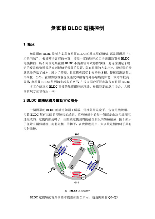
2 BLDC電機結構及驅動方式簡介一個簡單的BLDC的構造如圖1所示。
電機外層是定子,包含電機繞組。
多數BLDC都有三個Y型連接的繞組,這些繞組中的每一個都是由許多線圈互連組成的。
電機內部是轉子,由圍繞電機圓周的磁性相反的磁極組成。
圖1顯示了僅帶有兩個磁極(南北磁極)的轉子,在實際應用中,大多數電機的轉子具有多對磁極。
圖 1 BLDC基本結構[1]BLDC電機驅動電路的基本模型如圖2所示。
通過開關管Q0~Q5來控制電機三相繞組的通電狀態,開關管可以為IGBT或者功率MOS管。
其中位於上方即與電源正端連接的開關管稱為“上橋”,下方即與電源負端連接的開關管稱為“下橋”。
圖 2 BLDC電機驅動電路基本模型[2]例如,若Q1、Q4打開,其它開關管都關閉,則電流從電源正端經Q1、A 相繞組、C相繞組、Q4流回電源負端。
流過A、C相定子繞組的電流會產生一個磁場,由右手定則可知其方向與B相繞組平行。
由於轉子是永磁體,在磁場力的作用下會向著與定子磁場平行的方向旋轉,即轉到與B相繞組平行的位置,使轉子的北磁極與定子磁場的南磁極對齊。
類似地,打開不同的上、下橋臂MOS管組合,就可控制電流的流向,產生不同方向的磁場,使永磁體轉子轉到指定的位置。

无刷无霍尔BLCD电机控制•1.概述无霍尔的BLDC控制方案与有霍尔BLDC的基本原理相似,都是用所谓“六步换向法”,根据转子当前的位置,按照一定的顺序给定子绕组通电使BLDC电机转动。
所不同的是无霍尔BLDC不需要霍尔效应传感器,通过检测定子绕组的反电动势过零点来判断转子当前的位置。
与有霍尔的方案相比,最明显的优点就是降低了成本、减小了体积。
且电机引线从8根变为3根,使接线调试都大为简化。
另外,霍尔传感器容易受温度和磁场等外界环境的影响,故障率较高。
因此,无霍尔BLDC得到越来越多的应用,在很多场合正逐步取代有霍尔BLDC。
本文介绍三相BLDC电机的无霍尔控制理论。
根据特定的应用场合,具体的实现方法会有所不同。
2 .BLDC电机结构及驱动方式简介一个简单的BLDC的构造如图1所示。
电机外层是定子,包含电机绕组。
多数BLDC都有三个Y型连接的绕组,这些绕组中的每一个都是由许多线圈互连组成的。
电机内部是转子,由围绕电机圆周的磁性相反的磁极组成。
图1显示了仅带有两个磁极(南北磁极)的转子,在实际应用中,大多数电机的转子具有多对磁极。
图1BLCD基本结构BLDC电机驱动电路的基本模型如图2所示。
通过开关管Q0~Q5来控制电机三相绕组的通电状态,开关管可以为IGBT或者功率MOS管。
其中位于上方即与电源正端连接的开关管称为“上桥”,下方即与电源负端连接的开关管称为“下桥”。
图2BLCD电机驱动电路基本模型例如,若Q1、Q4打开,其它开关管都关闭,则电流从电源正端经Q1、A相绕组、C相绕组、Q4流回电源负端。
流过A、C相定子绕组的电流会产生一个磁场,由右手定则可知其方向与B相绕组平行。
由于转子是永磁体,在磁场力的作用下会向著与定子磁场平行的方向旋转,即转到与B相绕组平行的位置,使转子的北磁极与定子磁场的南磁极对齐。
类似地,打开不同的上、下桥臂MOS管组合,就可控制电流的流向,产生不同方向的磁场,使永磁体转子转到指定的位置。
MC9S12ZVM-Family Reference Manual HCS12MicrocontrollersTo provide the most up-to-date information, the document revision on the Internet is the most current. A printed copy may be an earlier revision. To verify you have the latest information available, refer to :.This document contains information for all constituent modules, with the exception of the S12Z CPU. For S12ZCPU information please refer to the CPU S12Z Reference Manual.S12ZVM32 and S12ZVM16 specific information is preliminary until these devices are qualified.The following revision history table summarizes changes contained in this document. The individual module sections contain revision history tables with more detailed information.Freescale Semiconductor reserves the right to make changes without further notice to any products herein. Freescale Semiconductor makes no warranty,representation or guarantee regarding the suitability of its products for any particular purpose, nor does Freescale Semiconductor assume any liability arising out of the application or use of any product or circuit, and specifically disclaims any and all liability, including without limitation consequential or incidental damages. “Typical” parameters that may be provided in Freescale Semiconductor data sheets and/or specifications can and do vary in different applications and actual performance may vary over time. All operating parameters, including “Typicals”, must be validated for each customer application by customer’s technical experts. Freescale Semiconductor does not convey any license under its patent rights nor the rights of others. Freescale Semiconductor products are not designed, intended, or authorized for use as components in systems intended for surgical implant into the body, or other applications intended to support or sustain life, or for any other application in which the failure of the Freescale Semiconductor product could create a situation where personal injury or death may occur. Should Buyer purchase or Table 0-1. Revision History DateRevision Description 12 Dec 2013 1.2 Replaced generic 8-channel TIM section with specific 4-channel TIM sectionTextual enhancements and corrections throughoutUpdated electrical parameter section and added parameters for temperataures up to 175°C- Added Table A-5- Merged Table A-8 and A-9 into Table A-9. Values updated. .- Table A-15. Parameter #2. max changed from 800uA to 1050uA- Table A-15. Inserted new C class parameter ISUPS at 85C. typ. 80uA- Appendices B,D and E. Updated parameter values based on characterization results.- Appendix C. Added parameter values for range above T=150°C- Table F-3. Merged rows 2a and 2b. Merged rows 6a and 6b.- Appendix G. Merged tables G-1 and G-2.- Tables H-1 and H-2 values updated.20 JAN 2014 1.3Updated Stop mode description for BDC enabled caseRemoved false reference to modified clock monitor assert frequencyUpdated electricals for 175°C Grade0- Removed temperature range disclaimer from electrical parameter spec.footer- Added sentence above table A-3- Table D-1. LINPHY parameters 12a and 12b replaced by 12a, 12b and 12c-- Table D-2. LINPHY wake up pulse over whole temperature range- Table E-1. FET gate charge spec. updated22 MAY2014 1.4Updated family derivative table for S12ZVML32, S12ZVM32 and S12ZVM16 devicesAdded 64KB, 32KB and 16KB derivative information to flash module chapterAdded pin routing options for S12ZVM32 and S12ZVM16 devicesAdded HV Phy information for the S12ZVM32 and S12ZVM16 derivativesUpdated Part ID assignment table and ordering information for S12ZVM32 and S12ZVM16Corrected PLL VCO maximum frequency specificationChanged V LVLSA maximum from 7V to 6.9VAdded electrical parameter for HD division ratio through the phase multiplexerCorrected preferred VRL reference from VRL_1 to VRL_0Included NVM timing parameters for the S12ZVM32 and S12ZVM16 devicesAdded GDU S12ZVM32 and S12ZVM16 specific differences and electrical specificationsAdded references to f WSTAT Added VDDX short circuit fall back current and temperature/input dependency specs.Chapter1Device Overview MC9S12ZVM-Family1.1Introduction . . . . . . . . . . . . . . . . . . . . . . . . . . . . . . . . . . . . . . . . . . . . . . . . . . . . . . . . . . . . . . . . . . 17 1.2Features . . . . . . . . . . . . . . . . . . . . . . . . . . . . . . . . . . . . . . . . . . . . . . . . . . . . . . . . . . . . . . . . . . . . . 181.2.1MC9S12ZVM-Family Member Comparison . . . . . . . . . . . . . . . . . . . . . . . . . . . . . . . . . 181.2.2Functional Differences Between N06E and 0N95G Masksets . . . . . . . . . . . . . . . . . . . . 191.2.3Functional Differences Between 1N95G and 0N95G Masksets . . . . . . . . . . . . . . . . . . . 20 1.3Chip-Level Features . . . . . . . . . . . . . . . . . . . . . . . . . . . . . . . . . . . . . . . . . . . . . . . . . . . . . . . . . . . . 20 1.4Module Features . . . . . . . . . . . . . . . . . . . . . . . . . . . . . . . . . . . . . . . . . . . . . . . . . . . . . . . . . . . . . . . 211.4.1S12Z Central Processor Unit (CPU) . . . . . . . . . . . . . . . . . . . . . . . . . . . . . . . . . . . . . . . . 211.4.2Embedded Memory . . . . . . . . . . . . . . . . . . . . . . . . . . . . . . . . . . . . . . . . . . . . . . . . . . . . . 221.4.3Clocks, Reset & Power Management Unit (CPMU) . . . . . . . . . . . . . . . . . . . . . . . . . . . . 231.4.4Main External Oscillator (XOSCLCP) . . . . . . . . . . . . . . . . . . . . . . . . . . . . . . . . . . . . . . 241.4.5Timer (TIM) . . . . . . . . . . . . . . . . . . . . . . . . . . . . . . . . . . . . . . . . . . . . . . . . . . . . . . . . . . . 241.4.6Pulse width Modulator with Fault protection (PMF) . . . . . . . . . . . . . . . . . . . . . . . . . . . . 241.4.7Programmable Trigger Unit (PTU) . . . . . . . . . . . . . . . . . . . . . . . . . . . . . . . . . . . . . . . . . 241.4.8LIN physical layer transceiver . . . . . . . . . . . . . . . . . . . . . . . . . . . . . . . . . . . . . . . . . . . . . 251.4.9Serial Communication Interface Module (SCI) . . . . . . . . . . . . . . . . . . . . . . . . . . . . . . . . 251.4.10Multi-Scalable Controller Area Network (MSCAN) . . . . . . . . . . . . . . . . . . . . . . . . . . . . 251.4.11Serial Peripheral Interface Module (SPI) . . . . . . . . . . . . . . . . . . . . . . . . . . . . . . . . . . . . . 261.4.12Analog-to-Digital Converter Module (ADC) . . . . . . . . . . . . . . . . . . . . . . . . . . . . . . . . . 261.4.13Supply V oltage Sensor (BATS) . . . . . . . . . . . . . . . . . . . . . . . . . . . . . . . . . . . . . . . . . . . . 261.4.14On-Chip V oltage Regulator system (VREG) . . . . . . . . . . . . . . . . . . . . . . . . . . . . . . . . . . 261.4.15Gate Drive Unit (GDU) . . . . . . . . . . . . . . . . . . . . . . . . . . . . . . . . . . . . . . . . . . . . . . . . . . 271.4.16Current Sense . . . . . . . . . . . . . . . . . . . . . . . . . . . . . . . . . . . . . . . . . . . . . . . . . . . . . . . . . . 271.4.17High V oltage Physical Interface (S12ZVM32, S12ZVM16) . . . . . . . . . . . . . . . . . . . . . . 27 1.5Block Diagram . . . . . . . . . . . . . . . . . . . . . . . . . . . . . . . . . . . . . . . . . . . . . . . . . . . . . . . . . . . . . . . . 28 1.6Device Memory Map . . . . . . . . . . . . . . . . . . . . . . . . . . . . . . . . . . . . . . . . . . . . . . . . . . . . . . . . . . . 291.6.1Flash Module . . . . . . . . . . . . . . . . . . . . . . . . . . . . . . . . . . . . . . . . . . . . . . . . . . . . . . . . . . 301.6.2Part ID Assignments . . . . . . . . . . . . . . . . . . . . . . . . . . . . . . . . . . . . . . . . . . . . . . . . . . . . 32 1.7Signal Description and Device Pinouts . . . . . . . . . . . . . . . . . . . . . . . . . . . . . . . . . . . . . . . . . . . . . 321.7.1Pin Assignment Overview . . . . . . . . . . . . . . . . . . . . . . . . . . . . . . . . . . . . . . . . . . . . . . . . 321.7.2Detailed External Signal Descriptions . . . . . . . . . . . . . . . . . . . . . . . . . . . . . . . . . . . . . . . 331.7.3Power Supply Pins . . . . . . . . . . . . . . . . . . . . . . . . . . . . . . . . . . . . . . . . . . . . . . . . . . . . . . 391.7.4Package and Pinouts . . . . . . . . . . . . . . . . . . . . . . . . . . . . . . . . . . . . . . . . . . . . . . . . . . . . 40 1.8Internal Signal Mapping . . . . . . . . . . . . . . . . . . . . . . . . . . . . . . . . . . . . . . . . . . . . . . . . . . . . . . . . . 461.8.1ADC Connectivity . . . . . . . . . . . . . . . . . . . . . . . . . . . . . . . . . . . . . . . . . . . . . . . . . . . . . . 471.8.2Motor Control Loop Signals . . . . . . . . . . . . . . . . . . . . . . . . . . . . . . . . . . . . . . . . . . . . . . 481.8.3Device Level PMF Connectivity . . . . . . . . . . . . . . . . . . . . . . . . . . . . . . . . . . . . . . . . . . . 481.8.4BDC Clock Source Connectivity . . . . . . . . . . . . . . . . . . . . . . . . . . . . . . . . . . . . . . . . . . . 481.8.5LINPHY Connectivity . . . . . . . . . . . . . . . . . . . . . . . . . . . . . . . . . . . . . . . . . . . . . . . . . . . 481.8.6HVPHY Connectivity . . . . . . . . . . . . . . . . . . . . . . . . . . . . . . . . . . . . . . . . . . . . . . . . . . . 481.8.7FTMRZ Connectivity . . . . . . . . . . . . . . . . . . . . . . . . . . . . . . . . . . . . . . . . . . . . . . . . . . . 491.8.8CPMU Connectivity . . . . . . . . . . . . . . . . . . . . . . . . . . . . . . . . . . . . . . . . . . . . . . . . . . . . 49 1.9Modes of Operation . . . . . . . . . . . . . . . . . . . . . . . . . . . . . . . . . . . . . . . . . . . . . . . . . . . . . . . . . . . . 491.9.1Chip Configuration Modes . . . . . . . . . . . . . . . . . . . . . . . . . . . . . . . . . . . . . . . . . . . . . . . 491.9.2Debugging Modes . . . . . . . . . . . . . . . . . . . . . . . . . . . . . . . . . . . . . . . . . . . . . . . . . . . . . . 501.9.3Low Power Modes . . . . . . . . . . . . . . . . . . . . . . . . . . . . . . . . . . . . . . . . . . . . . . . . . . . . . . 50 1.10Security . . . . . . . . . . . . . . . . . . . . . . . . . . . . . . . . . . . . . . . . . . . . . . . . . . . . . . . . . . . . . . . . . . . . . . 511.10.1Features . . . . . . . . . . . . . . . . . . . . . . . . . . . . . . . . . . . . . . . . . . . . . . . . . . . . . . . . . . . . . . 511.10.2Securing the Microcontroller . . . . . . . . . . . . . . . . . . . . . . . . . . . . . . . . . . . . . . . . . . . . . . 511.10.3Operation of the Secured Microcontroller . . . . . . . . . . . . . . . . . . . . . . . . . . . . . . . . . . . . 521.10.4Unsecuring the Microcontroller . . . . . . . . . . . . . . . . . . . . . . . . . . . . . . . . . . . . . . . . . . . . 521.10.5Reprogramming the Security Bits . . . . . . . . . . . . . . . . . . . . . . . . . . . . . . . . . . . . . . . . . . 531.10.6Complete Memory Erase . . . . . . . . . . . . . . . . . . . . . . . . . . . . . . . . . . . . . . . . . . . . . . . . . 53 1.11Resets and Interrupts . . . . . . . . . . . . . . . . . . . . . . . . . . . . . . . . . . . . . . . . . . . . . . . . . . . . . . . . . . . 541.11.1Resets . . . . . . . . . . . . . . . . . . . . . . . . . . . . . . . . . . . . . . . . . . . . . . . . . . . . . . . . . . . . . . . . 541.11.2Interrupt Vectors . . . . . . . . . . . . . . . . . . . . . . . . . . . . . . . . . . . . . . . . . . . . . . . . . . . . . . . 541.11.3Effects of Reset . . . . . . . . . . . . . . . . . . . . . . . . . . . . . . . . . . . . . . . . . . . . . . . . . . . . . . . . 57 1.12Module device level dependencies . . . . . . . . . . . . . . . . . . . . . . . . . . . . . . . . . . . . . . . . . . . . . . . . . 581.12.1CPMU COP Configuration . . . . . . . . . . . . . . . . . . . . . . . . . . . . . . . . . . . . . . . . . . . . . . . 581.12.2CPMU High Temperature Trimming . . . . . . . . . . . . . . . . . . . . . . . . . . . . . . . . . . . . . . . . 581.12.3Flash IFR Mapping . . . . . . . . . . . . . . . . . . . . . . . . . . . . . . . . . . . . . . . . . . . . . . . . . . . . . 58 1.13Application Information . . . . . . . . . . . . . . . . . . . . . . . . . . . . . . . . . . . . . . . . . . . . . . . . . . . . . . . . . 591.13.1ADC Calibration . . . . . . . . . . . . . . . . . . . . . . . . . . . . . . . . . . . . . . . . . . . . . . . . . . . . . . . 591.13.2SCI Baud Rate Detection . . . . . . . . . . . . . . . . . . . . . . . . . . . . . . . . . . . . . . . . . . . . . . . . . 591.13.3Motor Control Application Overview . . . . . . . . . . . . . . . . . . . . . . . . . . . . . . . . . . . . . . . 601.13.4BDCM Complementary Mode Operation . . . . . . . . . . . . . . . . . . . . . . . . . . . . . . . . . . . . 681.13.5BLDC Six-Step Commutation . . . . . . . . . . . . . . . . . . . . . . . . . . . . . . . . . . . . . . . . . . . . . 721.13.6PMSM Control . . . . . . . . . . . . . . . . . . . . . . . . . . . . . . . . . . . . . . . . . . . . . . . . . . . . . . . . . 741.13.7Power Domain Considerations . . . . . . . . . . . . . . . . . . . . . . . . . . . . . . . . . . . . . . . . . . . . 78Chapter2Port Integration Module (S12ZVMPIMV2)2.1Introduction . . . . . . . . . . . . . . . . . . . . . . . . . . . . . . . . . . . . . . . . . . . . . . . . . . . . . . . . . . . . . . . . . . 832.1.1Overview . . . . . . . . . . . . . . . . . . . . . . . . . . . . . . . . . . . . . . . . . . . . . . . . . . . . . . . . . . . . . 832.1.2Features . . . . . . . . . . . . . . . . . . . . . . . . . . . . . . . . . . . . . . . . . . . . . . . . . . . . . . . . . . . . . . 84 2.2External Signal Description . . . . . . . . . . . . . . . . . . . . . . . . . . . . . . . . . . . . . . . . . . . . . . . . . . . . . . 84 2.3Memory Map and Register Definition . . . . . . . . . . . . . . . . . . . . . . . . . . . . . . . . . . . . . . . . . . . . . . 882.3.1Register Map . . . . . . . . . . . . . . . . . . . . . . . . . . . . . . . . . . . . . . . . . . . . . . . . . . . . . . . . . . 892.3.2PIM Registers 0x0200-0x020F . . . . . . . . . . . . . . . . . . . . . . . . . . . . . . . . . . . . . . . . . . . . 932.3.3PIM Generic Registers . . . . . . . . . . . . . . . . . . . . . . . . . . . . . . . . . . . . . . . . . . . . . . . . . . 1012.3.4PIM Generic Register Exceptions . . . . . . . . . . . . . . . . . . . . . . . . . . . . . . . . . . . . . . . . . 109 2.4Functional Description . . . . . . . . . . . . . . . . . . . . . . . . . . . . . . . . . . . . . . . . . . . . . . . . . . . . . . . . . 1102.4.1General . . . . . . . . . . . . . . . . . . . . . . . . . . . . . . . . . . . . . . . . . . . . . . . . . . . . . . . . . . . . . . 1102.4.2Registers . . . . . . . . . . . . . . . . . . . . . . . . . . . . . . . . . . . . . . . . . . . . . . . . . . . . . . . . . . . . . 1112.4.3Pin I/O Control . . . . . . . . . . . . . . . . . . . . . . . . . . . . . . . . . . . . . . . . . . . . . . . . . . . . . . . . 1122.4.4Interrupts . . . . . . . . . . . . . . . . . . . . . . . . . . . . . . . . . . . . . . . . . . . . . . . . . . . . . . . . . . . . 1132.4.5Pin interrupts and Key-Wakeup (KWU) . . . . . . . . . . . . . . . . . . . . . . . . . . . . . . . . . . . . 1142.4.6Over-Current Interrupt . . . . . . . . . . . . . . . . . . . . . . . . . . . . . . . . . . . . . . . . . . . . . . . . . . 1152.5Initialization and Application Information . . . . . . . . . . . . . . . . . . . . . . . . . . . . . . . . . . . . . . . . . . 1152.5.1Port Data and Data Direction Register writes . . . . . . . . . . . . . . . . . . . . . . . . . . . . . . . . 1152.5.2Over-Current Protection on EVDD1 . . . . . . . . . . . . . . . . . . . . . . . . . . . . . . . . . . . . . . . 115Chapter3Memory Mapping Control (S12ZMMCV1)3.1Introduction . . . . . . . . . . . . . . . . . . . . . . . . . . . . . . . . . . . . . . . . . . . . . . . . . . . . . . . . . . . . . . . . . 1173.1.1Glossary . . . . . . . . . . . . . . . . . . . . . . . . . . . . . . . . . . . . . . . . . . . . . . . . . . . . . . . . . . . . . 1183.1.2Overview . . . . . . . . . . . . . . . . . . . . . . . . . . . . . . . . . . . . . . . . . . . . . . . . . . . . . . . . . . . . 1183.1.3Features . . . . . . . . . . . . . . . . . . . . . . . . . . . . . . . . . . . . . . . . . . . . . . . . . . . . . . . . . . . . . 1183.1.4Modes of Operation . . . . . . . . . . . . . . . . . . . . . . . . . . . . . . . . . . . . . . . . . . . . . . . . . . . . 1193.1.5Block Diagram . . . . . . . . . . . . . . . . . . . . . . . . . . . . . . . . . . . . . . . . . . . . . . . . . . . . . . . . 119 3.2External Signal Description . . . . . . . . . . . . . . . . . . . . . . . . . . . . . . . . . . . . . . . . . . . . . . . . . . . . . 119 3.3Memory Map and Register Definition . . . . . . . . . . . . . . . . . . . . . . . . . . . . . . . . . . . . . . . . . . . . . 1203.3.1Memory Map . . . . . . . . . . . . . . . . . . . . . . . . . . . . . . . . . . . . . . . . . . . . . . . . . . . . . . . . . 1203.3.2Register Descriptions . . . . . . . . . . . . . . . . . . . . . . . . . . . . . . . . . . . . . . . . . . . . . . . . . . . 120 3.4Functional Description . . . . . . . . . . . . . . . . . . . . . . . . . . . . . . . . . . . . . . . . . . . . . . . . . . . . . . . . . 1253.4.1Global Memory Map . . . . . . . . . . . . . . . . . . . . . . . . . . . . . . . . . . . . . . . . . . . . . . . . . . . 1253.4.2Illegal Accesses . . . . . . . . . . . . . . . . . . . . . . . . . . . . . . . . . . . . . . . . . . . . . . . . . . . . . . . 1273.4.3Uncorrectable ECC Faults . . . . . . . . . . . . . . . . . . . . . . . . . . . . . . . . . . . . . . . . . . . . . . . 128Chapter4Interrupt (S12ZINTV0)4.1Introduction . . . . . . . . . . . . . . . . . . . . . . . . . . . . . . . . . . . . . . . . . . . . . . . . . . . . . . . . . . . . . . . . . 1294.1.1Glossary . . . . . . . . . . . . . . . . . . . . . . . . . . . . . . . . . . . . . . . . . . . . . . . . . . . . . . . . . . . . . 1304.1.2Features . . . . . . . . . . . . . . . . . . . . . . . . . . . . . . . . . . . . . . . . . . . . . . . . . . . . . . . . . . . . . 1304.1.3Modes of Operation . . . . . . . . . . . . . . . . . . . . . . . . . . . . . . . . . . . . . . . . . . . . . . . . . . . . 1314.1.4Block Diagram . . . . . . . . . . . . . . . . . . . . . . . . . . . . . . . . . . . . . . . . . . . . . . . . . . . . . . . . 131 4.2External Signal Description . . . . . . . . . . . . . . . . . . . . . . . . . . . . . . . . . . . . . . . . . . . . . . . . . . . . . 132 4.3Memory Map and Register Definition . . . . . . . . . . . . . . . . . . . . . . . . . . . . . . . . . . . . . . . . . . . . . 1324.3.1Module Memory Map . . . . . . . . . . . . . . . . . . . . . . . . . . . . . . . . . . . . . . . . . . . . . . . . . . 1324.3.2Register Descriptions . . . . . . . . . . . . . . . . . . . . . . . . . . . . . . . . . . . . . . . . . . . . . . . . . . . 133 4.4Functional Description . . . . . . . . . . . . . . . . . . . . . . . . . . . . . . . . . . . . . . . . . . . . . . . . . . . . . . . . . 1384.4.1S12Z Exception Requests . . . . . . . . . . . . . . . . . . . . . . . . . . . . . . . . . . . . . . . . . . . . . . . 1384.4.2Interrupt Prioritization . . . . . . . . . . . . . . . . . . . . . . . . . . . . . . . . . . . . . . . . . . . . . . . . . . 1384.4.3Priority Decoder . . . . . . . . . . . . . . . . . . . . . . . . . . . . . . . . . . . . . . . . . . . . . . . . . . . . . . . 1394.4.4Reset Exception Requests . . . . . . . . . . . . . . . . . . . . . . . . . . . . . . . . . . . . . . . . . . . . . . . 1394.4.5Exception Priority . . . . . . . . . . . . . . . . . . . . . . . . . . . . . . . . . . . . . . . . . . . . . . . . . . . . . 1404.4.6Interrupt Vector Table Layout . . . . . . . . . . . . . . . . . . . . . . . . . . . . . . . . . . . . . . . . . . . . 140 4.5Initialization/Application Information . . . . . . . . . . . . . . . . . . . . . . . . . . . . . . . . . . . . . . . . . . . . . 1404.5.1Initialization . . . . . . . . . . . . . . . . . . . . . . . . . . . . . . . . . . . . . . . . . . . . . . . . . . . . . . . . . . 1404.5.2Interrupt Nesting . . . . . . . . . . . . . . . . . . . . . . . . . . . . . . . . . . . . . . . . . . . . . . . . . . . . . . 1414.5.3Wake Up from Stop or Wait Mode . . . . . . . . . . . . . . . . . . . . . . . . . . . . . . . . . . . . . . . . 142Chapter5Background Debug Controller (S12ZBDCV2)5.1Introduction . . . . . . . . . . . . . . . . . . . . . . . . . . . . . . . . . . . . . . . . . . . . . . . . . . . . . . . . . . . . . . . . . 1435.1.1Glossary . . . . . . . . . . . . . . . . . . . . . . . . . . . . . . . . . . . . . . . . . . . . . . . . . . . . . . . . . . . . . 1435.1.2Features . . . . . . . . . . . . . . . . . . . . . . . . . . . . . . . . . . . . . . . . . . . . . . . . . . . . . . . . . . . . . 1445.1.3Modes of Operation . . . . . . . . . . . . . . . . . . . . . . . . . . . . . . . . . . . . . . . . . . . . . . . . . . . . 1445.1.4Block Diagram . . . . . . . . . . . . . . . . . . . . . . . . . . . . . . . . . . . . . . . . . . . . . . . . . . . . . . . . 146 5.2External Signal Description . . . . . . . . . . . . . . . . . . . . . . . . . . . . . . . . . . . . . . . . . . . . . . . . . . . . . 147 5.3Memory Map and Register Definition . . . . . . . . . . . . . . . . . . . . . . . . . . . . . . . . . . . . . . . . . . . . . 1475.3.1Module Memory Map . . . . . . . . . . . . . . . . . . . . . . . . . . . . . . . . . . . . . . . . . . . . . . . . . . 1475.3.2Register Descriptions . . . . . . . . . . . . . . . . . . . . . . . . . . . . . . . . . . . . . . . . . . . . . . . . . . . 148 5.4Functional Description . . . . . . . . . . . . . . . . . . . . . . . . . . . . . . . . . . . . . . . . . . . . . . . . . . . . . . . . . 1525.4.1Security . . . . . . . . . . . . . . . . . . . . . . . . . . . . . . . . . . . . . . . . . . . . . . . . . . . . . . . . . . . . . 1525.4.2Enabling BDC And Entering Active BDM . . . . . . . . . . . . . . . . . . . . . . . . . . . . . . . . . . 1525.4.3Clock Source . . . . . . . . . . . . . . . . . . . . . . . . . . . . . . . . . . . . . . . . . . . . . . . . . . . . . . . . . 1535.4.4BDC Commands . . . . . . . . . . . . . . . . . . . . . . . . . . . . . . . . . . . . . . . . . . . . . . . . . . . . . . 1535.4.5BDC Access Of Internal Resources . . . . . . . . . . . . . . . . . . . . . . . . . . . . . . . . . . . . . . . . 1695.4.6BDC Serial Interface . . . . . . . . . . . . . . . . . . . . . . . . . . . . . . . . . . . . . . . . . . . . . . . . . . . 1725.4.7Serial Interface Hardware Handshake (ACK Pulse) Protocol . . . . . . . . . . . . . . . . . . . . 1755.4.8Hardware Handshake Abort Procedure . . . . . . . . . . . . . . . . . . . . . . . . . . . . . . . . . . . . . 1775.4.9Hardware Handshake Disabled (ACK Pulse Disabled) . . . . . . . . . . . . . . . . . . . . . . . . . 1785.4.10Single Stepping . . . . . . . . . . . . . . . . . . . . . . . . . . . . . . . . . . . . . . . . . . . . . . . . . . . . . . . 1795.4.11Serial Communication Timeout . . . . . . . . . . . . . . . . . . . . . . . . . . . . . . . . . . . . . . . . . . . 180 5.5Application Information . . . . . . . . . . . . . . . . . . . . . . . . . . . . . . . . . . . . . . . . . . . . . . . . . . . . . . . . 1805.5.1Clock Frequency Considerations . . . . . . . . . . . . . . . . . . . . . . . . . . . . . . . . . . . . . . . . . . 180Chapter6S12Z Debug (S12ZDBGV2) Module6.1Introduction . . . . . . . . . . . . . . . . . . . . . . . . . . . . . . . . . . . . . . . . . . . . . . . . . . . . . . . . . . . . . . . . . 1816.1.1Glossary . . . . . . . . . . . . . . . . . . . . . . . . . . . . . . . . . . . . . . . . . . . . . . . . . . . . . . . . . . . . . 1826.1.2Overview . . . . . . . . . . . . . . . . . . . . . . . . . . . . . . . . . . . . . . . . . . . . . . . . . . . . . . . . . . . . 1826.1.3Features . . . . . . . . . . . . . . . . . . . . . . . . . . . . . . . . . . . . . . . . . . . . . . . . . . . . . . . . . . . . . 1826.1.4Modes of Operation . . . . . . . . . . . . . . . . . . . . . . . . . . . . . . . . . . . . . . . . . . . . . . . . . . . . 1836.1.5Block Diagram . . . . . . . . . . . . . . . . . . . . . . . . . . . . . . . . . . . . . . . . . . . . . . . . . . . . . . . . 184 6.2External Signal Description . . . . . . . . . . . . . . . . . . . . . . . . . . . . . . . . . . . . . . . . . . . . . . . . . . . . . 1846.2.1External Event Input . . . . . . . . . . . . . . . . . . . . . . . . . . . . . . . . . . . . . . . . . . . . . . . . . . . 1846.2.2Profiling Output . . . . . . . . . . . . . . . . . . . . . . . . . . . . . . . . . . . . . . . . . . . . . . . . . . . . . . . 185 6.3Memory Map and Registers . . . . . . . . . . . . . . . . . . . . . . . . . . . . . . . . . . . . . . . . . . . . . . . . . . . . . 1856.3.1Module Memory Map . . . . . . . . . . . . . . . . . . . . . . . . . . . . . . . . . . . . . . . . . . . . . . . . . . 1856.3.2Register Descriptions . . . . . . . . . . . . . . . . . . . . . . . . . . . . . . . . . . . . . . . . . . . . . . . . . . . 188 6.4Functional Description . . . . . . . . . . . . . . . . . . . . . . . . . . . . . . . . . . . . . . . . . . . . . . . . . . . . . . . . . 2096.4.1DBG Operation . . . . . . . . . . . . . . . . . . . . . . . . . . . . . . . . . . . . . . . . . . . . . . . . . . . . . . . 2096.4.2Comparator Modes . . . . . . . . . . . . . . . . . . . . . . . . . . . . . . . . . . . . . . . . . . . . . . . . . . . . 2096.4.3Events . . . . . . . . . . . . . . . . . . . . . . . . . . . . . . . . . . . . . . . . . . . . . . . . . . . . . . . . . . . . . . . 2136.4.4State Sequence Control . . . . . . . . . . . . . . . . . . . . . . . . . . . . . . . . . . . . . . . . . . . . . . . . . 2156.4.5Trace Buffer Operation . . . . . . . . . . . . . . . . . . . . . . . . . . . . . . . . . . . . . . . . . . . . . . . . . 2166.4.6Code Profiling . . . . . . . . . . . . . . . . . . . . . . . . . . . . . . . . . . . . . . . . . . . . . . . . . . . . . . . . 2256.4.7Breakpoints . . . . . . . . . . . . . . . . . . . . . . . . . . . . . . . . . . . . . . . . . . . . . . . . . . . . . . . . . . 229 6.5Application Information . . . . . . . . . . . . . . . . . . . . . . . . . . . . . . . . . . . . . . . . . . . . . . . . . . . . . . . . 2306.5.1Avoiding Unintended Breakpoint Re-triggering . . . . . . . . . . . . . . . . . . . . . . . . . . . . . . 2306.5.2Debugging Through Reset . . . . . . . . . . . . . . . . . . . . . . . . . . . . . . . . . . . . . . . . . . . . . . . 2306.5.3Breakpoints from other S12Z sources . . . . . . . . . . . . . . . . . . . . . . . . . . . . . . . . . . . . . . 2316.5.4Code Profiling . . . . . . . . . . . . . . . . . . . . . . . . . . . . . . . . . . . . . . . . . . . . . . . . . . . . . . . . 231Chapter7ECC Generation Module (SRAM_ECCV1)7.1Introduction . . . . . . . . . . . . . . . . . . . . . . . . . . . . . . . . . . . . . . . . . . . . . . . . . . . . . . . . . . . . . . . . . 2337.1.1Features . . . . . . . . . . . . . . . . . . . . . . . . . . . . . . . . . . . . . . . . . . . . . . . . . . . . . . . . . . . . . 233 7.2Memory Map and Register Definition . . . . . . . . . . . . . . . . . . . . . . . . . . . . . . . . . . . . . . . . . . . . . 2337.2.1Register Summary . . . . . . . . . . . . . . . . . . . . . . . . . . . . . . . . . . . . . . . . . . . . . . . . . . . . . 2337.2.2Register Descriptions . . . . . . . . . . . . . . . . . . . . . . . . . . . . . . . . . . . . . . . . . . . . . . . . . . . 235 7.3Functional Description . . . . . . . . . . . . . . . . . . . . . . . . . . . . . . . . . . . . . . . . . . . . . . . . . . . . . . . . . 2397.3.1Aligned 2 and 4 Byte Memory Write Access . . . . . . . . . . . . . . . . . . . . . . . . . . . . . . . . 2407.3.2Other Memory Write Access . . . . . . . . . . . . . . . . . . . . . . . . . . . . . . . . . . . . . . . . . . . . 2407.3.3Memory Read Access . . . . . . . . . . . . . . . . . . . . . . . . . . . . . . . . . . . . . . . . . . . . . . . . . . 2417.3.4Memory Initialization . . . . . . . . . . . . . . . . . . . . . . . . . . . . . . . . . . . . . . . . . . . . . . . . . . 2417.3.5Interrupt Handling . . . . . . . . . . . . . . . . . . . . . . . . . . . . . . . . . . . . . . . . . . . . . . . . . . . . . 2417.3.6ECC Algorithm . . . . . . . . . . . . . . . . . . . . . . . . . . . . . . . . . . . . . . . . . . . . . . . . . . . . . . . 2427.3.7ECC Debug Behavior . . . . . . . . . . . . . . . . . . . . . . . . . . . . . . . . . . . . . . . . . . . . . . . . . . 242Chapter8S12 Clock, Reset and Power Management Unit (S12CPMU_UHV_V6)8.1Introduction . . . . . . . . . . . . . . . . . . . . . . . . . . . . . . . . . . . . . . . . . . . . . . . . . . . . . . . . . . . . . . . . . 2458.1.1Features . . . . . . . . . . . . . . . . . . . . . . . . . . . . . . . . . . . . . . . . . . . . . . . . . . . . . . . . . . . . . 2468.1.2Modes of Operation . . . . . . . . . . . . . . . . . . . . . . . . . . . . . . . . . . . . . . . . . . . . . . . . . . . . 2488.1.3S12CPMU_UHV_V6 Block Diagram . . . . . . . . . . . . . . . . . . . . . . . . . . . . . . . . . . . . . . 251 8.2Signal Description . . . . . . . . . . . . . . . . . . . . . . . . . . . . . . . . . . . . . . . . . . . . . . . . . . . . . . . . . . . . 2538.2.1RESET . . . . . . . . . . . . . . . . . . . . . . . . . . . . . . . . . . . . . . . . . . . . . . . . . . . . . . . . . . . . . . 2538.2.2EXTAL and XTAL . . . . . . . . . . . . . . . . . . . . . . . . . . . . . . . . . . . . . . . . . . . . . . . . . . . . . 2538.2.3VSUP — Regulator Power Input Pin . . . . . . . . . . . . . . . . . . . . . . . . . . . . . . . . . . . . . . 2538.2.4VDDA, VSSA — Regulator Reference Supply Pins . . . . . . . . . . . . . . . . . . . . . . . . . . 2538.2.5VDDX, VSSX— Pad Supply Pins . . . . . . . . . . . . . . . . . . . . . . . . . . . . . . . . . . . . . . . . 2538.2.6BCTL— Base Control Pin for external PNP . . . . . . . . . . . . . . . . . . . . . . . . . . . . . . . . . 2548.2.7VSS1,2 — Core Ground Pins . . . . . . . . . . . . . . . . . . . . . . . . . . . . . . . . . . . . . . . . . . . . 2548.2.8VDD— Core Logic Supply Pin . . . . . . . . . . . . . . . . . . . . . . . . . . . . . . . . . . . . . . . . . . . 2548.2.9VDDF— NVM Logic Supply Pin . . . . . . . . . . . . . . . . . . . . . . . . . . . . . . . . . . . . . . . . . 2548.2.10API_EXTCLK — API external clock output pin . . . . . . . . . . . . . . . . . . . . . . . . . . . . . 2548.2.11TEMPSENSE — Internal Temperature Sensor Output V oltage . . . . . . . . . . . . . . . . . . 254。
无刷直流BLDC电机控制解决方案无刷直流(BLDC)电机正迅速成为要求高可靠性,高效率和高功率体积比的应用的自然选择。
这些电机在很宽的速度范围内提供大量的扭矩,并且与有刷电机具有相似的扭矩和速度性能曲线特性(尽管有刷电机可提供更大的静止扭矩)。
BLDC电机由于消除了传统直流电机换向时使用的电刷而具有显着的可靠性。
刷子磨损,降低了电机的性能,最终必须更换。
相反,在额定参数范围内运行时,BLDC 电机的预期寿命可超过10,000小时或更长。
与传统装置相比,这种寿命以及随后的维护和备件成本的降低可以抵消电机的较高初始成本。
BLDC电机正在进入最具成本意识的应用领域。
例如,在汽车领域,BLDC电机的使用正在飙升。
汽车制造商尤其被电机在机械工作中转换电能的效率所吸引,这有助于降低对车辆电力系统的需求(图1)。
根据分析师IMS的研究,到2018年,6亿只BLDC电机将用于内燃机驱动的轻型车辆,而2011年则为2亿只。
(BLDC电机的大型版本在电动和混合动力汽车中已经很常见。
)图1:BLDC电机,如用于水泵的这种装置,正在取代汽车应用中的传统电机(Melexis提供)。
BLDC电机的这种兴趣促使芯片供应商为该单元的电子控制系统开发定制的单片芯片。
本文将详细介绍BLDC 电机控制芯片- 用于驱动逆变桥的设备,最终激活电机线圈并控制速度和方向等参数。
减少霍尔传感器故障飞兆半导体公司拥有BLDC电机控制的悠久历史,最近推出的FCM8201芯片仍在继续。
该器件专为感应BLDC 电机控制而设计。
(传感电机需要霍尔效应传感器来指示线圈位置以辅助电子换向序列)。
FCM8201的关键技术进步是它可以选择脉冲宽度调制(PWM)模式。
有两种PWM模式可供选择:正弦波模式和方波模式。
方波模式包括PWM-PWM和PWM-ON技术,可提高电机驱动效率。
Fairchild解释说,该器件还内置霍尔信号调节电路,可为每个传感器信号输入产生3至6μs的“去抖”时间。
120°方波无传感器BLDC电机控制器1、概述本应用笔记介绍了如何使用“端电压法”来实现120°方波无传感器BLDC电机控制器的设计。
采用“端电压法”来检测无传感器BLDC电机转子的位置,具有电路简单和程序算法简单的优点,系统响应速度快。
端电压的过零点就是电机的换相点,与构建电机虚拟中性点的检测方式相比,无需软件延时30°电角度,降低了软件编写的难度。
本设计中采用C8051F330的片上比较器来检查BLDC电机端电压的过零点,从而获得转子的位置。
针对不同的无传感器BLDC电机,在此设计的基础上适当地修改一些参数,都能很好地满足对BLDC驱动的要求。
C8051F330是美国芯科实验室设计的一款高速51内核的MCU,它是传统51 MCU的改良产品,完全兼容传统51 MCU。
C8051F330指令运行的峰值高达25MHZ,具有20个引脚,8K flash,768RAM,3个PCA模块,4个16位定时器,16通道10位ADC,AD转换速度高达200ksps,1通道10位DAC,1个片上比较器和1个片上温度传感器,以及丰富的通信接口:I2C、SPI和UART,QFN20小封装。
所需硬件●SMC0901开发板(见图4)●航模BLDC电机:D2632-1000(12VDC,4对极,额定带载转速5800RPM)●12V DC电源图4 SMC0901开发板该方案能实现的功能●无传感器BLDC电机120°方波驱动●正反转控制●调速范围:2000RPM ~ 6500RPM(机械转速),精度≤2%●PID转速闭环控制●比较器法检测电机端电压过零点●保护功能:过流保护、堵转保护和缺相保护●出现故障后立即进入保护状态,3秒后进入自恢复起动,重新开始运行(堵转和缺相情况除外)该方案优势:●采用“端电压法”,使用MCU内置的比较器检测端电压过零点,效率更高,成本更低,能很好地适应比较高速的无传感器BLDC电机调速系统●自动相位控制,完全由硬件自动完成,无需软件干预●参数调整简单,以适应不同的无传感器BLDC电机系统●能提供软、硬件参考设计●适用于泵类和风机类负载的应用2、系统介绍1)“端电压法”A) U、V、W三相的理想相电压波形图如图1、图2、图3所示:B) U、W两相电压合成的波形图如图5所示。