BDR6122T-无线充电专用驱动芯片
- 格式:pdf
- 大小:1.06 MB
- 文档页数:12
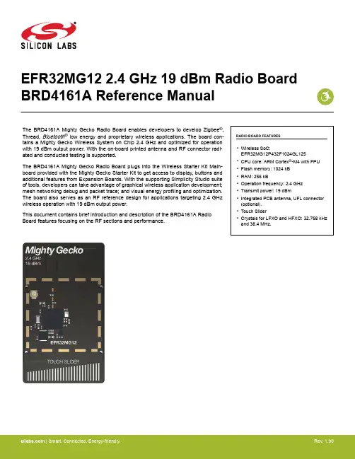
EFR32MG12 2.4 GHz 19 dBm Radio Board BRD4161A Reference ManualRADIO BOARD FEATURES•Wireless SoC:EFR32MG12P432F1024GL125•CPU core: ARM Cortex ®-M4 with FPU •Flash memory: 1024 kB •RAM: 256 kB•Operation frequency: 2.4 GHz •Transmit power: 19 dBm•Integrated PCB antenna, UFL connector (optional).•Touch Slider•Crystals for LFXO and HFXO: 32.768 kHz and 38.4 MHz.The BRD4161A Mighty Gecko Radio Board enables developers to develop Zigbee ®, Thread,Bluetooth ® low energy and proprietary wireless applications. The board con-tains a Mighty Gecko Wireless System on Chip 2.4 GHz and optimized for operation with 19 dBm output power. With the on-board printed antenna and RF connector radi-ated and conducted testing is supported.The BRD4161A Mighty Gecko Radio Board plugs into the Wireless Starter Kit Main-board provided with the Mighty Gecko Starter Kit to get access to display, buttons and additional features from Expansion Boards. With the supporting Simplicity Studio suite of tools, developers can take advantage of graphical wireless application development; mesh networking debug and packet trace; and visual energy profiling and optimization. The board also serves as an RF reference design for applications targeting 2.4 GHz wireless operation with 19 dBm output power.This document contains brief introduction and description of the BRD4161A Radio Board features focusing on the RF sections and performance.| Smart. Connected. Energy-friendly.Rev. 1.00Introduction 1. IntroductionThe EFR32 Mighty Gecko Radio Boards provide a development platform (together with the Wireless Starter Kit Mainboard) for the Silicon Labs EFR32 Mighty Gecko Wireless System on Chips and serve as reference designs for the matching network of the RF inter-face.The BRD4161A Radio Board is designed to operate in the 2400-2483.5 MHz band with the RF matching network optimized to operate with 19 dBm output power.To develop and/or evaluate the EFR32 Mighty Gecko, the BRD4161A Radio Board can be connected to the Wireless Starter Kit Main-board to get access to display, buttons and additional features from Expansion Boards and also to evaluate the performance of the RF interface.2. Radio Board Connector2.1 IntroductionThe board-to-board connector scheme allows access to all EFR32MG12 GPIO pins as well as the RESETn signal. For more informa-tion on the functions of the available pin functions, see the EFR32MG12 data sheet.2.2 Radio Board Connector Pin AssociationsThe figure below shows the pin mapping on the connector to the radio pins and their function on the Wireless Starter Kit Mainboard.GNDF9 / PA3 / VCOM_RTS 3v3VCOM_RTS / PA3 / P36P200Upper RowNC / P38NC / P40PF9 / P42PF11 / P44DEBUG.TMS_SWDIO / PF1 / F0DISP_ENABLE / PD15 / F14UIF_BUTTON0 / PF6 / F12UIF_LED1 / PF4 / F10VCOM_CTS / PA2 / F8DEBUG.RESET / RADIO_#RESET / F4DEBUG.TDO_SWO / PF2 / F2DISP_SI / PC6 / F16VCOM_TXD / PA0 / F6PTI_DATA / PB12 / F20DISP_EXTCOMIN / PD13 / F18USB_VBUS5VBoard ID SCLGNDBoard ID SDAUSB_VREG F7 / PA1 / VCOM_RXD F5 / PA5 / VCOM_ENABLE F3 / PF3 / DEBUG.TDIF1 / PF0 / DEBUG.TCK_SWCLK P45 / PF12P43 / PF10P41 / PF8P39 / NC P37/ PB10 / SENSOR_ENABLE F11 / PF5 / UIF_LED1F13 / PF7 / UIF_BUTTON1F15 / PC8 / DISP_SCLK F17 / PD14 / DISP_SCS F19 / PB13 / PTI_FRAME F21 / PB11 / PTI_CLK GND VMCU_IN PD8 / P0P201Lower RowPD9 / P2PD10 / P4PD11 / P6GNDNCP35 / PA2 / VCOM_CTS P7 / PA9P5 / PA8P3 / PA7P1 / PA6P33 / PA0 / VCOM_TXD P31 / PK2P29 / PK0P27 / PJ14P25 / PI2P23 / PI0P21 / PF14P19 / NC P17 / PC5P15 / PB9P13 / PC11P11 / PB7P9 / PB6VCOM_RXD / P34 / P34BODEN / P32PK1/ P30PJ15 / P28PI3 / P26PI1 / P24PF15 / P22PF13 / P20NC / P18PC4 / P16PB8 / P14PC10 / P12PC9 / P10PD12 / P8Figure 2.1. BRD4161A Radio Board Connector Pin MappingRadio Board Connector3. Radio Board Block Summary3.1 IntroductionThis section gives a short introduction to the blocks of the BRD4161A Radio Board.3.2 Radio Board Block DiagramThe block diagram of the EFR32MG Radio Board is shown in the figure below.Figure 3.1. BRD4161A Block Diagram3.3 Radio Board Block Description3.3.1 Wireless MCUThe BRD4161A Mighty Gecko Radio Board incorporates an EFR32MG12P432F1024GL125 Wireless System on Chip featuring 32-bit Cortex®-M4 with FPU core, 1024 kB of flash memory and 256 kB of RAM and a 2.4 GHz band transceiver with output power up to 19 dBm. For additional information on the EFR32MG12P432F1024GL125, refer to the EFR32MG12 Data Sheet.3.3.2 LF Crystal Oscillator (LFXO)The BRD4161A Radio Board has a 32.768 kHz crystal mounted.3.3.3 HF Crystal Oscillator (HFXO)The BRD4161A Radio Board has a 38.4 MHz crystal mounted.| Smart. Connected. Energy-friendly.Rev. 1.00 | 33.3.4 Matching Network for 2.4 GHzThe BRD4161A Radio Board incorporates a 2.4 GHz matching network which connects the 2.4 GHz TRX pin of the EFR32MG12 to the one on-board printed Inverted-F antenna. The component values were optimized for the 2.4 GHz band RF performace and current con-sumption with 19 dBm output power.For detailed description of the matching network, see Chapter 4.2.1 Description of the 2.4 GHz RF Matching.3.3.5 Inverted-F AntennaThe BRD4161A Radio Board includes a printed Inverted-F antenna (IFA) tuned to have close to 50 Ohm impedance at the 2.4 GHz band.For detailed description of the antenna see Chapter 4.5 Inverted-F Antenna.3.3.6 UFL ConnectorTo be able to perform conducted measurements, Silicon Labs added an UFL connector to the Radio Board. The connector allows an external 50 Ohm cable or antenna to be connected during design verification or testing.Note: By default the output of the matching network is connected to the printed Inverted-F antenna by a series component. It can be connected to the UFL connector as well through a series 0 Ohm resistor which is not mounted by default. For conducted measurements through the UFL connector the series component to the antenna should be removed and the 0 Ohm resistor should be mounted (see Chapter 4.2 Schematic of the RF Matching Network for further details).3.3.7 Radio Board ConnectorsTwo dual-row, 0.05” pitch polarized connectors make up the EFR32MG Radio Board interface to the Wireless Starter Kit Mainboard. For more information on the pin mapping between the EFR32MG12P432F1024GL125 and the Radio Board Connector, refer to Chapter 2.2 Radio Board Connector Pin Associations.3.3.8 Capacitive Touch SliderThe touch slider (T2) utilizes the capacitive touch capability of the Capacitance Sense Module of the EFR32MG12. The slider interpo-lates 4 separate pads to find the exact position of a finger.The figure below shows the pin mapping of the touch slider to the Wireless SoC.Wireless SoCFigure 3.2. Touch Slider Pin MappingRev. 1.00 | 44. RF Section4.1 IntroductionThis section gives a short introduction to the RF section of the BRD4161A.4.2 Schematic of the RF Matching NetworkThe schematic of the RF section of the BRD4161A Radio Board is shown in the following figure.2.4 GHz Matching 2.4 GHz RF OutputSelection & Inverted-F AntennaFigure 4.1. Schematic of the RF Section of the BRD4161A4.2.1 Description of the 2.4 GHz RF MatchingThe 2.4 GHz matching connects the 2G4RF_IOP pin to the on-board printed Inverted-F Antenna. The 2G4RF_ION pin is connected to ground. For higher output powers (13 dBm and above), besides the impedance matching circuitry, it is recommended to use additional harmonic filtering as well at the RF output. The targeted output power of the BRD4161A board is 19 dBm. Therefore, the RF output of the IC is connected to the antenna through a four-element impedance matching and harmonic filter circuitry.For conducted measurements the output of the matching network can also be connected to the UFL connector by removing the series R1 component between the antenna and the output of the matching and adding a 0 Ohm resistor to the R2 resistor position between the output of the matching and the UFL connector.4.3 RF Section Power SupplyOn the BRD4161A Radio Board the power supply pins of the RF section (RFVDD, PAVDD) are directly connected to the output of the on-chip DC-DC converter. This way, by default, the DC-DC converter provides 1.8 V for the entire RF section (for details, see the sche-matic of the BRD4161A).4.4 Bill of Materials for the 2.4 GHz MatchingThe Bill of Materials of the 2.4 GHz matching network of the BRD4161A Radio Board is shown in the following table.| Smart. Connected. Energy-friendly.Rev. 1.00 | 5Table 4.1. Bill of Materials for the BRD4161A 2.4GHz RF Matching Network4.5 Inverted-F AntennaThe BRD4161A Radio Board includes an on-board printed Inverted-F Antenna tuned for the 2.4 GHz band. Due to the design restric-tions of the Radio Board, the input of the antenna and the output of the matching network can't be placed directly next to each other. As a result, a 50 Ohm transmission line was necessary to connect them. With the actual line length the impedance of the antenna at the double-harmonic frequency is transformed closer to a "critical load impedance range" resulting in the radiated level of the harmonic increases.To reduce the harmonic radiation a tuning component was used between the matching network output and the antenna input. For the actual Radio Board design (with the actual transmission line length) a small value inductor was used (instead of the R1 resistor with value of 1.8 nH) to transform the impedance at the double-frequency harmonic away from the critical region while keeping the impe-dance at the funamental close to 50 Ohm. With this the suppression of the radiated double-frequency harmonic increases by approxi-mately 3-4 dB. The resulting impedance and reflection measured at the output of the matcing network are shown in the following figure. As it can be observed the impedance is close to 50 Ohm (the reflection is better than -10 dB) for the entire 2.4 GHz band.Figure 4.2. Impedance and Reflection of the Inverted-F Antenna of the BRD4161A Board Measured from the Matching Output Note: The same value and type of 1.8 nH inductor was used as the one in the matching network (L1). | Smart. Connected. Energy-friendly.Rev. 1.00 | 65. Mechanical DetailsThe BRD4161A Mighty Gecko Radio Board is illustrated in the figures below.Figure 5.1. BRD4161A Top View24 mmConnectorConnector Figure 5.2. BRD4161A Bottom ViewMechanical DetailsRev. 1.00 | 7EMC Compliance 6. EMC Compliance6.1 IntroductionCompliance of the fundamental and harmonic levels is tested against the following standards:• 2.4 GHz:•ETSI EN 300-328•FCC 15.2476.2 EMC Regulations for 2.4 GHz6.2.1 ETSI EN 300-328 Emission Limits for the 2400-2483.5 MHz BandBased on ETSI EN 300-328 the allowed maximum fundamental power for the 2400-2483.5 MHz band is 20 dBm EIRP. For the unwan-ted emissions in the 1 GHz to 12.75 GHz domain the specified limit is -30 dBm EIRP.6.2.2 FCC15.247 Emission Limits for the 2400-2483.5 MHz BandFCC 15.247 allows conducted output power up to 1 Watt (30 dBm) in the 2400-2483.5 MHz band. For spurious emmissions the limit is -20 dBc based on either conducted or radiated measurement, if the emission is not in a restricted band. The restricted bands are speci-fied in FCC 15.205. In these bands the spurious emission levels must meet the levels set out in FCC 15.209. In the range from 960 MHz to the frequency of the 5th harmonic it is defined as 0.5 mV/m at 3 m distance (equals to -41.2 dBm in EIRP).Additionally, for spurious frequencies above 1 GHz, FCC 15.35 allows duty-cycle relaxation to the regulatory limits. For the EmberZNet PRO the relaxation is 3.6 dB. Therefore, the -41.2 dBm limit can be modified to -37.6 dBm.If operating in the 2400-2483.5 MHz band the 2nd, 3rd and 5th harmonics can fall into restricted bands. As a result, for those the -37.6 dBm limit should be applied. For the 4th harmonic the -20 dBc limit should be applied.6.2.3 Applied Emission Limits for the 2.4 GHz BandThe above ETSI limits are applied both for conducted and radiated measurements.The FCC restricted band limits are radiated limits only. Besides that, Silicon Labs applies those to the conducted spectrum i.e., it is assumed that, in case of a custom board, an antenna is used which has 0 dB gain at the fundamental and the harmonic frequencies. In that theoretical case, based on the conducted measurement, the compliance with the radiated limits can be estimated.The overall applied limits are shown in the table below.Table 6.1. Applied Limits for Spurious Emissions for the 2.4 GHz Band | Smart. Connected. Energy-friendly.Rev. 1.00 | 87. RF Performance7.1 Conducted Power MeasurementsDuring measurements, the EFR32MG Radio Board was attached to a Wireless Starter Kit Mainboard which was supplied by USB. The voltage supply for the Radio Board was 3.3 V.7.1.1 Conducted Measurements in the 2.4 GHz bandThe BRD4161A board was connected directly to a Spectrum Analyzer through its UFL connector (the R1 component was removed and a 0 Ohm resistor was soldered to the R2 resistor position). During measurements, the voltage supply for the board was 3.3 V provided by the mainboard. The supply for the radio (RFVDD) was 1.8 V provided by the on-chip DC-DC converter, the supply for the power amplifier (PAVDD) was 3.3 V (for details, see the schematic of the BRD4161A). The transceiver was operated in continuous carrier transmission mode. The output power of the radio was set to 19 dBm.The typical output spectrum is shown in the following figure.Figure 7.1. Typical Output Spectrum of the BRD4161AAs it can be observed, the fundamental is slightly lower than 19 dBm limit and the strongest unwanted emission is the double-frequency harmonic and it is under the -37.6 dBm applied limit.Note: The conducted measurement is performed by connecting the on-board UFL connector to a Spectrum Analyzer through an SMA Conversion Adapter (P/N: HRMJ-U.FLP(40)). This connection itself introduces approximately 0.3 dB insertion loss.RF PerformanceRev. 1.00 | 97.2 Radiated Power MeasurementsDuring measurements, the EFR32MG Radio Board was attached to a Wireless Starter Kit Mainboard which was supplied by USB. The voltage supply for the Radio Board was 3.3 V. The radiated power was measured in an antenna chamber by rotating the DUT 360degrees with horizontal and vertical reference antenna polarizations in the XY , XZ and YZ cuts. The measurement axes are shown inthe figure below.Figure 7.2. DUT: Radio Board with the Wireless Starter Kit Mainboard (Illustration)Note: The radiated measurement results presented in this document were recorded in an unlicensed antenna chamber. Also the radi-ated power levels may change depending on the actual application (PCB size, used antenna, and so on). Therefore, the absolute levels and margins of the final application are recommended to be verified in a licensed EMC testhouse.7.2.1 Radiated Measurements in the 2.4 GHz bandFor the transmitter antenna the on-board printed Inverted-F antenna of the BRD4161A board was used (the R1 component was moun-ted). During measurements, the board was attached to a Wireless Starter Kit Mainboard (BRD4001 (Rev. A02) ) which was supplied through USB. During the measurements the voltage supply for the board was 3.3 V provided by the mainboard. The supply for the radio (RFVDD) was 1.8 V provided by the on-chip DC-DC converter, the supply for the power amplifier (PAVDD) was 3.3 V (for details, see the schematic of the BRD4161A). The transceiver was operated in continuous carrier transmission mode. The output power of the radio was set to 19 dBm based on the conducted measurement.The results are shown in the table below.Table 7.1. Maximums of the measured radiated powers in EIRP [dBm]As it can be observed, thanks to the high gain of the Inverted-F antenna, the level of the fundamental is higher than 19 dBm. The stron-gest harmonic is the double-frequency one and thanks to the additional suppression provided by the instead of the R1 resistor its level is under -50 dBm.RF PerformanceEMC Compliance Recommendations 8. EMC Compliance Recommendations8.1 Recommendations for 2.4 GHz ETSI EN 300-328 complianceAs it was shown in the previous chapter, the radiated power of the fundamental of the BRD4161A Mighty Gecko Radio Board complies with the 20 dBm limit of the ETSI EN 300-328 in case of the conducted measurement but due to the high antenna gain the radiated power is higher than the limit by 2 dB. In order to comply, the output power should be reduced (with different antennas, depending on the gain of the used antenna, the necessary reduction can be different). The harmonic emissions are under the -30 dBm limit. Although the BRD4161A Radio Board has an option for mounting a shielding can, that is not required for the compliance.8.2 Recommendations for 2.4 GHz FCC 15.247 complianceAs it was shown in the previous chapter, the radiated power of the fundamental of the BRD4161A Mighty Gecko Radio Board complies with the 30 dBm limit of the FCC 15.247. The harmonic emissions are under the -37.6 dBm applied limit both in case of the conducted and the radiated measurements. Although the BRD4161A Radio Board has an option for mounting a shielding can, that is not required for the compliance.Document Revision History 9. Document Revision HistoryTable 9.1. Document Revision HistoryBoard Revision History 10. Board Revision HistoryTable 10.1. BRD4161A Radio Board RevisionsErrata 11. ErrataThere are no known errata at present.Table of Contents1. Introduction (1)2. Radio Board Connector (2)2.1 Introduction (2)2.2 Radio Board Connector Pin Associations (2)3. Radio Board Block Summary (3)3.1 Introduction (3)3.2 Radio Board Block Diagram (3)3.3 Radio Board Block Description (3)3.3.1 Wireless MCU (3)3.3.2 LF Crystal Oscillator (LFXO) (3)3.3.3 HF Crystal Oscillator (HFXO) (3)3.3.4 Matching Network for 2.4 GHz (4)3.3.5 Inverted-F Antenna (4)3.3.6 UFL Connector (4)3.3.7 Radio Board Connectors (4)3.3.8 Capacitive Touch Slider (4)4. RF Section (5)4.1 Introduction (5)4.2 Schematic of the RF Matching Network (5)4.2.1 Description of the 2.4 GHz RF Matching (5)4.3 RF Section Power Supply (5)4.4 Bill of Materials for the 2.4 GHz Matching (5)4.5 Inverted-F Antenna (6)5. Mechanical Details (7)6. EMC Compliance (8)6.1 Introduction (8)6.2 EMC Regulations for 2.4 GHz (8)6.2.1 ETSI EN 300-328 Emission Limits for the 2400-2483.5 MHz Band (8)6.2.2 FCC15.247 Emission Limits for the 2400-2483.5 MHz Band (8)6.2.3 Applied Emission Limits for the 2.4 GHz Band (8)7. RF Performance (9)7.1 Conducted Power Measurements (9)7.1.1 Conducted Measurements in the 2.4 GHz band (9)7.2 Radiated Power Measurements (10)7.2.1 Radiated Measurements in the 2.4 GHz band (10)8. EMC Compliance Recommendations (11)8.1 Recommendations for 2.4 GHz ETSI EN 300-328 compliance (11)8.2 Recommendations for 2.4 GHz FCC 15.247 compliance (11)9. Document Revision History (12)10. Board Revision History (13)11. Errata (14)Table of Contents (15)Silicon Laboratories Inc.400 West Cesar Chavez Austin, TX 78701USASimplicity StudioOne-click access to MCU and wireless tools, documentation, software, source code libraries & more. Available for Windows, Mac and Linux!IoT Portfolio /IoTSW/HW/simplicityQuality/qualitySupport and CommunityDisclaimerSilicon Labs intends to provide customers with the latest, accurate, and in-depth documentation of all peripherals and modules available for system and software implementers using or intending to use the Silicon Labs products. Characterization data, available modules and peripherals, memory sizes and memory addresses refer to each specific device, and "Typical" parameters provided can and do vary in different applications. Application examples described herein are for illustrative purposes only. Silicon Labs reserves the right to make changes without further notice and limitation to product information, specifications, and descriptions herein, and does not give warranties as to the accuracy or completeness of the included information. Silicon Labs shall have no liability for the consequences of use of the information supplied herein. This document does not imply or express copyright licenses granted hereunder to design or fabricate any integrated circuits. The products are not designed or authorized to be used within any Life Support System without the specific written consent of Silicon Labs. A "Life Support System" is any product or system intended to support or sustain life and/or health, which, if it fails, can be reasonably expected to result in significant personal injury or death. Silicon Labs products are not designed or authorized for military applications. Silicon Labs products shall under no circumstances be used in weapons of mass destruction including (but not limited to) nuclear, biological or chemical weapons, or missiles capable of delivering such weapons.Trademark InformationSilicon Laboratories Inc.® , Silicon Laboratories®, Silicon Labs®, SiLabs® and the Silicon Labs logo®, Bluegiga®, Bluegiga Logo®, Clockbuilder®, CMEMS®, DSPLL®, EFM®, EFM32®, EFR, Ember®, Energy Micro, Energy Micro logo and combinations thereof, "the world’s most energy friendly microcontrollers", Ember®, EZLink®, EZRadio®, EZRadioPRO®, Gecko®, ISOmodem®, Precision32®, ProSLIC®, Simplicity Studio®, SiPHY®, Telegesis, the Telegesis Logo®, USBXpress® and others are trademarks or registered trademarks of Silicon Labs. ARM, CORTEX, Cortex-M3 and THUMB are trademarks or registered trademarks of ARM Holdings. Keil is a registered trademark of ARM Limited. All other products or brand names mentioned herein are trademarks of their respective holders.。

昂科发布软件更新支持Nation国民技术的N32WB452系列低功耗蓝牙芯片N32WB452LEQ6的烧录芯片烧录行业领导者-昂科技术近日发布最新的烧录软件更新及新增支持的芯片型号列表,其中Nation国民技术的N32WB452系列低功耗蓝牙芯片N32WB452LEQ6的烧录已经被昂科的通用烧录平台AP8000所支持。
N32WB452系列BLE5.0微控制器产品采用32位ARM Cortex-M4加32位ARM Cortex-M0双内核构架,其中32bit ARM Cortex-M0核专用于处理BLE5.0射频电路及蓝牙协议,通过内部高速总线,由ARM Cortex-M4核进行配置。
ARM Cortex-M4核作为应用处理器,支持浮点运算单元(FPU)和数字信号处理(DSP)指令,支持并行计算指令,最高工作主频144MHz,集成高达512KB加密存储Flash并支持多用户分区管理,最大144KB SRAM。
内置一个内部高速AHB总线,二个低速外设时钟总线APB及总线矩阵,最多支持65个通用I/O,提供丰富的高性能模拟接口,包括2个12bit 5Msps ADC,最多支持16个外部输入通道、2个1Msps12bit DAC、多达18通道电容式触摸按键,同时提供多种数字通信接口,包括7个U(S)ART、4个I2C、3个SPI、1个USB 2.0设备、2个CAN 2.0B通信接口,1个数字视频接口(DVP),1个SDIO接口,内置密码算法硬件加速引擎,支持多种国际及国密算法硬件加速。
N32WB452系列产品提供了符合BLE 5.0的无线连接能力,稳定工作于-40°C至+85°C 的温度范围,供电电压1.8V至3.6V,提供多种功耗模式供用户选择,符合低功耗应用的要求。
该系列产品提供QFN48、QFN64和QFN88封装。
根据不同的封装形式,器件中的外设配置不尽相同。
这些丰富的外设配置,使得N32WB452系列BLE5.0微控制器芯片适合于智能门锁、智能穿戴、智能标签、智能家居、物联网及移动互联等多种应用场合。
WD6122 红外遥控发射电路WD6122 芯片是通用红外遥控发射集成电路,采用CMOS 工艺制造,最多可外接64个按键,并有三组双重按键。
封装形式为SOP-24和SOP-20。
一.特点z低压CMOS 工艺制造z工作电压范围宽z通过外部接法最多可产生65536种用户码z可通过SEL管脚选择,最多可支持128+ 6条指令码z SOP-24、SOP-20、COB封装形式可选二. 应用范围z VCD、DVD 播放机、电视机、组合音响设备、电视机顶盒三. 产品规格分类z WD6122-001:SEL2接GND ,ROM中数据为0z WD6122-002:SEL2接VDD,用户专用模式四. 结构框图WD6122 红外遥控发射电路五. 管脚图及管脚说明1. 管脚图2. 管脚说明管脚号 符号 输入输出 功能描述23、24、1~6 KI0-KI7 I 键扫描输入端7 REM O数据输出管脚(遥控输出)8 Vdd 电源正极9 SEL I 选择管脚10 OSCO O 振荡器管脚(输出)11 OSCI I 振荡器管脚(输入)12 Vss 电源负极13 LMP O 输出LED指示(呈闪烁状态)21~14 KI/O0~KI/O7I/O 键扫描输入/输出管脚22 CCS I 键扫描输入WD6122 红外遥控发射电路六. 功能说明1. 编码方式WD6122时被传送。
码型结构如下:引导码由一个9ms的载波波形和4.5ms的关断时间构成,它作为随后发射的码的引导,这样当接收系统是由微处理器构成的时候,能更有效地处理码的接收与检测及其它各项控制之间的时序关系。
编码采用脉冲位置调制方式(PPM)。
利用脉冲之间的时间间隔来区分“0”和“1”。
每次8位的码被传送之后,它们的反码也被传送,减少了系统的误码率。
2.键盘输入矩阵WD6122键盘输入矩阵请参考下图:3.按键输入WD6122 在键扫描输入端KI0~KI7 和键扫描定时信号输入/输出端KI/O0~KI/O7构成的8×8 矩阵上共设置64 个按键。
规格说明书SGD5141XX无线充电(带锂电保护)接收芯片版本1.5 安 浩 芯保留不预先通知而修改此文件的权利目录1.概述 (3)2.特性 (3)3.引脚说明 (4)4.功能模块框图 (5)5.封装尺寸图 (6)6.编号说明 (7)7.应用电路图 (8)8.无线充电 (9)9.通信功能 (9)10.状态指示 (9)11.过温保护功能 (10)12.过流、短路保护和自动恢复功能 (10)13.过放电保护功能 (11)14.极限工作条件 (11)15.电气参数 (12)16.修改记录 (13)1. 概述SGD5141是一款无线充电接收+锂电保护芯片,其集成通讯、高频整流、频率控制、充电状态指示、过温保护、过流保护、锂电保护等功能,外围器件精简到只需要一个小电容,带上模拟混合数字的技术,使整机可靠性更高,应用更加灵活简洁。
在小体积的产品上应用更加有优势和效率更高。
应用范围广:数码产品(智能手表、手环、耳机……),以及各类需要防水、外观讲究和充电方便的手持产品。
2. 特性◆内置的功率级采用低电阻NMOS FET技术确保高效率与低功耗◆内置模拟+数字解调,减少外围器件,通讯更加可靠灵活◆充电状态和电池状态可以给指示◆免调试,自动连接◆自动功率控制◆过热保护功能(OTP)◆欠压保护功能(UVLO)◆过流保护功能(OCP)◆短路保护功能(SCP)◆外围电路简单到一个电容,体积小,安装方便◆静态电流小于6uA,过放电保护后电流小于1uA◆电池保护功能◆充电电压检测精度高◆锂电保护◆多芯片并联,增加充电电流3. 引脚说明SOT23-6:DFN6L(2*2)4. 功能模块框图5. 封装尺寸图SOT23-6DFN6L(2mm*2mm)DFN6L(0202X0.75-0.65) 封装尺寸图6.编号说明封装形式:S表示SOT23-6充电电流:1表示100mA充电结束电压:4表示4.2V表示无线接收IC品牌7.应用电路图单芯片电路图并联芯片电路1、C1电容尽量靠近芯片,到芯片VDD和GND的走线尽量短和粗,如果电池的引线比较长,那么要加大C1的容量2、C1电容请使用NPO电容3、电池的引线到芯片的VDD和GND尽量短和粗4、由于采用的是高频磁耦合传输电能,为了减少高频的趋肤效应,用铜线绕制线圈时,可以采用多股线,画PCB或FPC时用双面板而且走线尽量宽5、LAYOUT时注意,跟芯片底部金属和GND引脚相连的铜皮尽量大和厚,目的这样可以帮助芯片散热和减低导通内阻,从而增加转换效率和提高系统的稳定性8.无线充电芯片内部集成无线充电管理电路,VCHG端口跟接收线圈相连,发射线圈发生的交变磁场,会使放在附近的接收线圈接收到AC信号,芯片内部的高压整流电路会把接收到AC信号整理成DC电源提供给电池充电,当电池电压小于2.7V时实行涓流充电,大于2.7V实现恒流充电,充电到电池电压大约4.15V时,会转成类似恒压的涓充,充电到4.2V时结束充电,充电结束电压精度是1%。
rt06122snhec03规格书引言一、产品简介rt06122snhec03是一款多功能设备,具备高性能和稳定性。
它可以广泛应用于各个行业,如工业自动化、通信、电子等领域。
该产品采用先进的技术和材料,具有出色的耐用性和可靠性。
二、外观设计rt06122snhec03外观简洁大方,采用了现代化设计理念。
机身采用高强度材料制成,具有良好的耐磨性和防护性能。
产品的尺寸合理,便于携带和安装。
外观颜色多样,可根据客户需求进行定制。
三、性能参数1. 处理器性能:rt06122snhec03配备了高性能的处理器,能够快速处理大量数据和复杂计算,确保设备的高效运行。
2. 存储容量:rt06122snhec03内置大容量存储器,能够存储大量数据和文件,满足不同应用场景的需求。
3. 通信接口:rt06122snhec03具备多种通信接口,如以太网、USB、RS232等,便于与其他设备进行连接和数据传输。
4. 电源管理:rt06122snhec03采用先进的电源管理技术,具有低功耗和高效能的特点,能够提供稳定可靠的电源供应。
5. 温度范围:rt06122snhec03能够在广泛的温度范围内正常工作,适应各种环境条件。
6. 抗震能力:rt06122snhec03具备良好的抗震能力,能够在恶劣的工作环境下保持稳定运行。
四、功能特点1. 多任务处理:rt06122snhec03能够同时处理多个任务,提高工作效率。
2. 数据加密:rt06122snhec03支持数据加密功能,确保数据的安全性和机密性。
3. 远程管理:rt06122snhec03具备远程管理功能,可以通过网络远程监控和管理设备,方便用户进行远程操作。
4. 高精度测量:rt06122snhec03具有高精度的测量能力,能够准确测量各种物理量。
5. 多种应用场景:rt06122snhec03适用于多种应用场景,如工业自动化控制、实验测量、通信设备等。
五、应用领域rt06122snhec03可以广泛应用于各个行业领域,如工业控制系统、通信设备、电子仪器仪表等。


快充识别芯片工作原理宝子们!今天咱们来唠唠那个超酷的快充识别芯片到底是咋工作的呢?这快充啊,现在可是咱们手机充电的救星,而这个识别芯片就像是背后的神秘小助手。
咱先来说说快充的需求是咋来的。
你想啊,以前咱们手机充电那叫一个慢,充个电等得花儿都谢了。
所以呢,快充技术就应运而生啦。
但是呢,不同的设备它能接受的充电功率是不一样的,就像有的人只能吃一小碗饭,你给一大盆就不行了。
这时候快充识别芯片就闪亮登场啦。
这个芯片啊,就像是一个超级聪明的小门卫。
它住在充电线或者手机的充电接口附近呢。
当你把充电器插到手机上的时候,电流就像一群小蚂蚁一样跑过来啦。
这时候芯片就开始工作啦。
它首先得知道这个充电器是个啥来头,是普通的那种慢吞吞的充电器呢,还是超级快充的那种厉害角色。
芯片它有自己的一套小办法来识别哦。
它就像是一个有超能力的小侦探。
它能检测到充电器传过来的一些小信号。
比如说,快充充电器会发送一种特殊的电压或者电流的波动模式。
这个芯片呢,就对这些波动超级敏感,就像小狗闻到肉骨头的香味一样。
一旦它发现这个特殊的波动,就知道,来的是快充充电器呢。
那它识别出来之后又干啥呢?它就像是一个小指挥官啦。
它会告诉手机的电池管理系统,说:“兄弟,来的是快充,咱可以敞开肚皮接收啦。
”然后呢,电池管理系统就会调整自己的状态,就像打开了高速充电的大门。
它会允许更大的电流进入电池,这样手机就能快速地充电啦。
但是,如果来的是普通充电器,这个芯片也不会搞错哦。
它就会告诉电池管理系统:“哎,来的是个小功率的,咱悠着点充。
”这样就可以避免因为电流过大而损坏电池啦。
而且呢,这个快充识别芯片还很贴心呢。
它会时刻关注着充电的情况。
就像一个小护士照顾病人一样。
如果在快充的过程中出现了什么问题,比如说电流突然不稳定啦,或者温度过高啦。
这个芯片就会赶紧发出警报。
它会告诉电池管理系统:“不好啦,有点不对劲,咱们得调整一下。
”然后电池管理系统就会根据芯片的提示来调整充电的功率或者停止充电,这样就可以保证充电过程的安全啦。
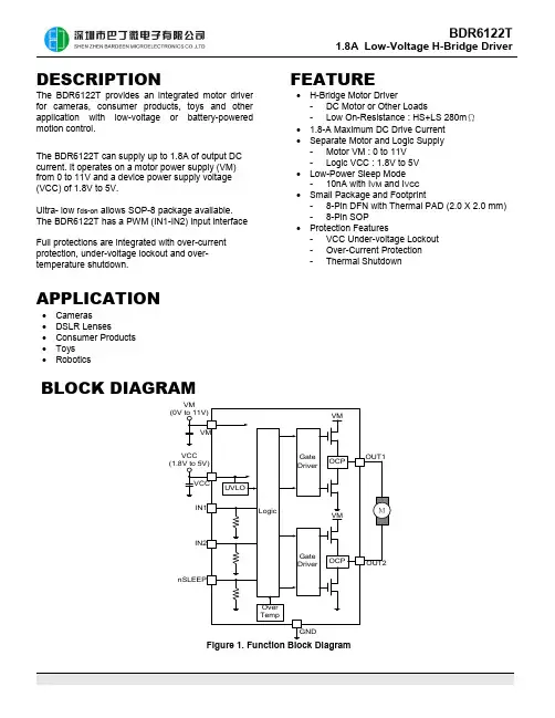
BDR6122T 1.8A Low-Voltage H-Bridge DriverDESCRIPTIONThe BDR6122T provides an integrated motor driver for cameras, consumer products, toys and other application with low-voltage or battery-powered motion control.The BDR6122T can supply up to 1.8A of output DC current. It operates on a motor power supply (VM) from 0 to 11V and a device power supply voltage (VCC) of 1.8V to 5V.Ultra- low r ds-on allows SOP-8 package available. The BDR6122T has a PWM (IN1-IN2) input interface Full protections are integrated with over-current protection, under-voltage lockout and over-temperature shutdown.APPLICATION∙Cameras∙DSLR Lenses∙Consumer Products∙Toys∙Robotics FEATURE∙H-Bridge Motor Driver- DC Motor or Other Loads- Low On-Resistance : HS+LS 280mΩ∙ 1.8-A Maximum DC Drive Current∙Separate Motor and Logic Supply- Motor VM : 0 to 11V- Logic VCC : 1.8V to 5V∙Low-Power Sleep Mode- 10nA with I VM and I VCC∙Small Package and Footprint- 8-Pin DFN with Thermal PAD (2.0 X 2.0 mm) - 8-Pin SOP∙Protection Features- VCC Under-voltage Lockout- Over-Current Protection- Thermal ShutdownBLOCK DIAGRAMFigure 1. Function Block DiagramAPPLICATION CIRCUITFigure 2. Schematic of Application*C3 is optional for better performance. Details are referred to at the chapter “Power Supply Recommendations”.PIN DESCRIPTIONVM OUT1OUT2GNDIN2IN1nSLEEP VCC DFN-8VM OUT1OUT2GNDIN2IN1nSLEEP VCC SOP-8FUNCTION DESCRIPTIONBRIDGE CONTROLThe BDR6122T is controlled using a PWM input interface, also called an IN-IN interface. Each output is controlled by aPROTECTION MANAGEMENTFUNCTIONAL MODESThe BDR6122T is active unless the nSLEEP pin is brought logic low. In sleep mode, the H-bridge FETs are disabledPOWER SUPPLY RECOMMENDATIONSHaving appropriate local bulk capacitance is an important factor in motor-drive system design. It is generally beneficial to have more bulk capacitance.The amount of local bulk capacitor needed depends on the following factors ,∙The highest current required by the motor system.∙The power-supply capacitance and ability to source current∙The amount of parasitic inductance between the power supply and motor system∙The acceptable voltage ripple∙The type of motor used (brushed dc, brushless dc, stepper)∙The motor braking methodThe inductance between the power supply and motor drive system limits the rate at which current can change from the power supply. If the local bulk capacitance is too small, the system responds to excessive current demands or dumps from the motor with a change in voltage. When adequate bulk capacitance is used, the motor voltage remains stable and high current can be quickly supplied.The voltage rating for bulk capacitors should be higher than the operating voltage, to provide margin for cases whenFigure 3. Motor Driver System with External Power SupplyPCB LAYOUTThe VM and VCC should be bypassed to GND using low-ESR ceramic capacitors with recommended value of 0.1µF. These capacitors should be placed as close to the VM and VCC as possible with a thick trace or ground plane connection to GND.0.1uF0.1uFELECTRICALCHARACTERISTICSTIMING REQUIREMENTST A =25℃IN1IN2OUT1OUT2OUTxTYPICAL OPERATING CHARACTERISTICSFigure 12. 50% Duty Cycle , Forward Direction Figure 13. 20% Duty Cycle , Forward Direction Figure 14. 50% Duty Cycle , Reverse Direction Figure 15. 20% Duty Cycle , Reverse DirectionPACKAGE INFORMATION 8-PIN, DFNNote:Refer to JEDEC MO-2298 PINS, SOP, 150MILNotes:1. Refer to JEDEC MS-012AA2. All dimensions are in millimeter。
PT2262,2272无线发射接收芯片这是一种目前用途非常广泛的200米四键遥控模块,常用于报警器设防、车库门遥控、摩托车、汽车的防盗报警等,这类用途要求遥控器的遥控距离并不远,一般50米足够了,但要求:遥控模块价格低廉,发射机手柄体积小巧、外观精致,耗电尽可能省,工作稳定可靠。
这里提供的发射机体积非常小巧,体积只有58x38x8毫米,采用桃木花纹的优质塑料外壳,带保险盖,防止误碰按键,天线拉出时长13厘米,遥控器只有20克。
上图为发射器外形,面板上有A、B、C、D四位操纵按键及一个发射指示灯。
发射机内部采用进口声表谐振器稳频,频率一致性非常好,稳定度极高,工作频率315MHZ频率稳定度优于10-5,使用中无需调整频点,特别适合多发一收等无线电遥控系统使用,而目前市场上的无线电遥控模块一般仍采用LC振荡器,稳定度及一致性较差,即使采用高品质微调电容,温度变化及震动也很难保证已调试好的频点不会发生偏移,造成发射距离缩短。
接收模块采用SMD贴片工艺制造生产,为超再生接收方式,它内含放大整形及解码电路,使用极为方便。
1、天线输入端有选频电路,而不依赖1/4波长天线的选频作用,控制距离较近时可以剪短甚至去掉外接天线92、接收电路自身辐射极小,加上电路模块背面网状接地铜箔的屏蔽作用,可以减少自身振荡的泄漏和外界干扰信号的侵入。
3、接收机采用高精度带骨架的铜芯电感将频率调整到315M后封固,这与采用可调电容调整接收频率的电路相比,温度、湿度稳定性及抗机械振动性能都有极大改善。
可调电容调整精度较低,只有3/4圈的调整范围,而可调电感可以做到多圈调整。
可调电容调整完毕后无法封固,因为无论导体还是绝缘体,各种介质的靠近或侵入都会使电容的容量发生变化,进而影响接收频率。
另外未经封固的可调电容在受到振动时定片和动片之间发生位移;温度变化时热胀冷缩会使定片和动片间距离改变;湿度变化因介质变化改变容量;长期工作在潮湿环境中还会因定片和动片的氧化改变容量,这些都会严重影响接收频率的稳定性,而采用可调电感就可解决这些问题,因为电感可以在调整完毕后进行封固,绝缘体封固剂不会使电感量发生变化,而且由于采用贴片工艺,所以即使强烈震动也不必担心接收频点漂移,接收电路的接收带宽约500KHz,产品出厂时已经将中心频率调整在315MHz,接收芯片上的微调电感约有5MHz频率的可调范围,使用时不要轻易变动,以免影响性能。
BDR2L00Half-Bridge DriverDESCRIPTIONThe BDR2L00 is a single Phase MOSFET gate driver optimized to drive the gates of both high-side and low-side power MOSFETs.FEATURES∙ Drive two N-MOSFETs∙ High-Frequency operation (Up to 1MHz) ∙ PWM input capable of 3.3V and 5V ∙ Fast output rise timeAPPLICATION CIRCUIT SOP8/DFN8:PIN CONFIGURATIONABSOLUTE MAXIMUM RATINGSStresses exceeding the absolute maximum ratings may damage the device or make the function abnormal. All the voltage parameters are absolute voltages referenced to IC PGND unless otherwise stated in the table.ELECTRICAL CHARACTERISTICSAPPLICATION INFORMATIONTheory of OperationThe BDR2L00 is an integrated driver and boot diode module designed for N+N half bridge driver. A single PWM input signal is all that is required to properly drive the high−side and low−side MOSFETs.Low−Side DriverThe low-side driver is designed to drive a ground−referenced low R DS(on)N−Channel MOSFET. The voltage rail for the low−side driver is internally connected to VCC and GND.High−Side DriverThe high-side driver is designed to drive a floating low RDS(ON) N−channel MOSFET. The gate voltage for the high side driver is developed by a bootstrap circuit referenced to Switch Node (PHASE) pin.The bootstrap circuit is comprised of the internal diode and an external bootstrap capacitor. When the BDR2L00 is starting up, the PHASE pin is at ground, so the bootstrap capacitor will charge up to VCC through the bootstrap diode. When the PWM input goes high, the high−side driver will begin to turn on the high−side MOSFET using the stored charge of the bootstrap capacitor. As the high−side MOSFET turns on, the PHASE pin will rise. When the high−side MOSFET is fully on, the switch node will be at 12V, and the BST pin will be at 5V plus the charge of the bootstrap capacitor (approaching 17V).The bootstrap capacitor is recharged when the switch node goes low during the next cycle.Safety Timer and Overlap Protection CircuitIt is very important that MOSFETs in a synchronous buck regulator do not both conduct at the same time. Excessive shoot−through or cross conduction can damage the MOSFETs, and even a small amount of cross conduction will cause a decrease in the power conversion efficiency.The BDR2L00 prevents cross conduction by monitoring the status of the MOSFETs and applying the appropriate amount of “dead−time” or the time between the turn off of one MOSFET and the turn on of the other MOSFET.When the PWM input pin goes high, the gate of the low−side MOSFET will go low after a propagation delay. The time it takes for the low−side MOSFET to turn off is dependent on the total charge on the low−side MOSFET gate. Likewise, when the PWM input pin goes low, the gate of the high−side MOSFET will go low after the propagation delay. The time to turn off the high−side MOSFET is dependent on the total gate charge of the high−side MOSFET.Enable (Only for DFN8)If EN pin is low level, whatever the PWM pin is high or low, all circuits are shutdown. If EN pin is high level, the outputs are controlled by PWM pin.Thermal ShutdownIf the driver temperature exceeds 170°C, the part will enter thermal shutdown and turn off both MOSFETs. Once the temperature falls below 150°C, the part will resume normal operation.Power Supply DecouplingThe BDR2L00 can source and sink relatively large current to the gate pins of the MOSFETs. In order to maintain a constant and stable supply voltage (VCC) a low ESR capacitor should be placed near the power and ground pins. A 2.2uF to 10uF multilayer ceramic capacitor (MLCC) is usually sufficient.Bootstrap CircuitThe bootstrap circuit uses a charge storage capacitor (C BST). The bootstrap capacitor must have a voltage rating that is able to withstand twice the maximum supply voltage. A minimum 16 V rating is recommended. A bootstrap capacitance greater than 680nF and a minimum 16V rating is recommended. A good quality ceramic capacitor should be used.PACKAGE INFORMATION 8 PINS, SOP, 150MIL8-PINS, DFN, 3X3。
VR422CAT VR622CAT6 Hookups without a Cable Box/Direct Broadcast SystemThe basic VCR/TV connection – antenna/cable to VCR to TV – is shown below. If you have a Cable Box or a Direct Broadcast System, please see pages eight-nine. If you have a Stereo TV, please see page 10.After you hook up the VCR, go to page 11 to turn on the VCR.(The VR622CAT is illustrated here. The VR422CAT has single AUDIO IN/OUT jacks.)TV)Cable (75 ohm)Back of VCR1Disconnect the antenna or cable from your TV.2Connect the antenna or cable to the ANT(enna) IN Jack of your VCR.3Connect the supplied black RF coaxial cable to the OUT Jack on the back of the VCR and to the ANTENNA IN Jack on the TV. (You may use either a snap-on type (supplied) or screw-on type of coaxial cable, whichever you prefer.)5Set the CH3/CH4 switch on the back of the VCR to CH3 or CH4, whichever channel is not used or least used in your area. Set the TV to the same channel.For example, when playing a tape, if the CH3/CH4 switch is set to CH3, the TV should be on channel 03.Hookups without a Cable Box/Direct Broadcast System (cont’d) 74Plug in the power cords of the TV and the VCR.You are ready to turn on the VCR. Please go to page 11 before turning on the VCR.8 Hookups with a Cable Box/Direct Broadcast SystemThere are two ways to connect your Cable Box/DBS to the VCR. With this connection:q You may view any channel.q You must select channels at the Cable Box/DBS. You can not change channels at the VCR.q You may not view a channel other than the one you are recording.q You may not program channels at the VCR.q You can only program a timer recording for one channel at a time. Set the TV and the VCR to the Cable Box/DBS output channel (channel 03 or 04). Set the CH3/CH4 switch on the back of the VCR to the same channel. Set your Cable Box/DBS to the channel you want to record. When you enter the channel you want to record in a timerrecording, select channel 03 or 04 (the Cable Box/DBS output channel). (This is step 5 on page 34.) Leave the Cable Box/DBS on for a timer recording.Recording/Viewing Any Channel1With the VCR on and in VCR position (the VCR light will appear on the display panel),set the VCR to the Cable Box/DBS output channel (03 or 04).2Set the TV to the same channel to which you set the VCR. Set the CH3/CH4switch on the back of the VCR to the same channel.3Select the channel you want to view/record at the Cable Box/DBS.1Connect a Cable signal to the IN Jack on the Cable Box/DBS.2Use the supplied black RF coaxial cable to connect the OUT Jack on the Cable Box/DBS to the ANT(enna) IN Jack on the VCR.3Use a second RF coaxial cable (not supplied) to connect the OUT Jack on the VCR to the TV’s ANTENNA IN Jack.Hookups with a Cable Box/Direct Broadcast System (cont’d) 9With this connection:q You may watch one channel while recording another.q You may not record scrambled channels.Recording One Channel/Watching Another1Put the Cable Box/DBS on the same channel as the VCR’s CH3/CH4switch. Set the TV to the Cable Box/DBS output channel (03 or 04).Then, with the VCR in VCR position (the VCR light will appear on the display panel), use the CH(annel) o /p buttons to select the channel you want to record at the VCR. Start the recording.2Press the VCR/TV button once to put the VCR in TV position.(The VCR light will disappear.)3Select the channel you want to watch at the Cable Box/DBS.4To return to the channel you are recording, set the Cable Box/DBS to the same channel as the VCR’s CH3/CH4 switch. Press the VCR/TV button so that the VCR is in VCR position again. The VCR light will appear on the display panel. The channel you are recording will appear on the TV screen. Press the STOP/p button to stop recording.1Connect a Cable signal to the VCR’s ANT(enna) IN Jack.2Use the supplied black RF coaxial cable to connect the OUT Jack on the VCR to the IN Jack on the Cable Box/DBS.3Use a second RF coaxial cable (not supplied) to connect the OUT Jack on the Cable Box/DBS to the ANTENNA IN Jack on the TV.10 Hookups with a Stereo TVq Audio and Video cables are not supplied.1Connect the antenna or cable to the ANT(enna) IN Jack on the back of the VCR.2Connect a video cable to the yellow VIDEO OUT Jack on the back of the VCR. Then, connect the other end of the video cable to the VIDEO IN Jack on your TV.3If you have the VR622CAT,connect a stereo audio cable to the red and white AUDIO OUT Jacks on the back of the VCR. Then, connect the other end of the audio cable to the AUDIO IN Jacks on your TV.If you have the VR422CAT, connect an audio cable to the white AUDIO OUT Jack on the back of the VCR. Then, connect the other end of the audio cable to the AUDIO IN Jack on your TV. If your TV has Right and Left AUDIO IN Jacks, you must use a “Y” splitter audio cable as illustrated to deliver audio to the TV’s right and left channels. This hookup will not give you stereo sound. To get stereo sound, use the connections on pages six - seven and select the channel to be viewed at the TV (with the VCR turned off).4Turn on your TV,making sure it is in Line Input mode. This might be referred to as the TV’s Audio/Video In channel or the Auxiliary In channel. Please refer to your TV owner’s manual for details.antenna or cable to Audio and Video INJacks on TVVR622CATAudio CableAudio and Video IN Jacks on TVFront Panel 27 PAUSE ButtonUse to watch TV (changing channels at the TV) or to watch one program while recording another. When the VCR light does not appear on the display panel, the VCR is in TV position.Press to access or remove theon-screen status display. Details are on page 25. Press to exit on-screen menus.28 Rear PanelDetails are on page 37.If you connect other equipment to the AUDIO and VIDEO IN jacks on the back of the VCR, select channel 001 (AV REAR) at the VCR. This allows you to view or hear the materials playing on the other equipment.ANT(enna) IN Jack Connect your antenna or cable here. Details are on pages six-10.Use the supplied black RFcoaxial cable to connectthis jack to the ANTEN-NA IN Jack on your TV,Cable Box, or DirectBroadcast System. Detailsare on pages six-nine.VCR.1Make the connections shown above.Rerecording (Tape Duplication) 373VCR 2 will record your tape. Insert a blank tape in VCR 2.The VCR must be in VCR position. (The VCR light will appear on the display panel. If it does not, press the VCR/TV button once.)4Turn on the TV and set it to channel 03 or 04,whichever channel the CH3/CH4 switch on VCR 2 is set to.5Point the remote control at VCR 2. Press the VCR but-ton, then press Number buttons 0, 0, 1 or 0, 0, 2. (See Helpful Hints at right.)6Press the SPEED button to select SP or SLP at VCR 2.7Press the PLAY button on VCR 1 and the RECORD but-ton on VCR 2 at the same time.To stop recording, press the STOP/EJECT button on VCR 1, then press the STOP/EJECT button on VCR 2.2VCR 1 will play your tape. Put a prerecorded tape in VCR 1.q Audio and Video cables are not supplied.1. Audio cables from AUDIO OUT Jacks of VCR 1 to AUDIO IN Jacks of VCR 22. Video cable from VIDEO OUT Jack of VCR 1 to VIDEO IN Jack of VCR 2from the OUT jack of VCR 2 to the TV’s ANTENNA IN JackThe instructions on this page show you how to copy tapes. The illustration uses two VR622CAT VCRs. Different VCRs may operate differently. To duplicate a tape, make the connections shown, then follow steps 1-7.。
rt06122snhec03规格书
rt06122snhec03 是一款电子产品,主要用于数据传输与处理。
该产品具有高速传输、稳定性能、小巧便携和抗干扰能力强等特性,广泛应用于工业自动化、智能家居、医疗设备和消费电子等领域。
产品名称:rt06122snhec03,类型:电子产品。
该产品的主要功能是数据传输与处理。
技术参数方面,rt06122snhec03 具有以下特点:传输速率100Mbps、工作温度0-50 摄氏度、存储温度-20-70 摄氏度、电源5V DC、尺寸100mm x 60mm x 30mm。
这些参数使得该产品在各种环境下都能稳定工作,满足不同场景的需求。
在产品特性方面,rt06122snhec03 具备高速传输、稳定性能、小巧便携和抗干扰能力强等特点。
高速传输能够保证数据在短时间内的快速传输;稳定性能让产品在各种环境下都能保持稳定的工作状态;小巧便携的尺寸使得产品方便携带,便于安装和使用;抗干扰能力强可以保证产品在复杂环境中正常工作。
rt06122snhec03 广泛应用于工业自动化、智能家居、医疗设备和消费电子等领域。
在工业自动化领域,该产品可以实现设备之间的数据传输与处理,提高生产效率;在智能家居中,它可以实现家居设备的联网控制,提高生活品质;在医疗设备中,rt06122snhec03 可以实现医疗数据的快速传输,提高诊断效率;在消费电子中,该产品可以实现多种设备之间的数据交互,丰富用户体验。
FM01BTS/FM01BTD文件编号:S&CIC1270)充电器驱动IC功能描述FM01BTS/FM01BTD (文件编号:S&CIC1270) 充电器驱动IC电气参数VDD=5V , Vout=5V Ta=25℃, 除非另有说明。
参数 符号 测试条件 最小值 典型值 最大值单位开启电压 VDDon VDD 上升从0开始 5 5.8 -- V 关闭电压 VDDoff 开关打开之后VDD 下降2.5 2.8 -- V 工作电流 IDD 正常工作 -- 1 3 mA 启动电流 IDDst开关打开之前-- 30 50 uA效率 η -- -- 78 -- %前沿消隐时间 -- -- -- 600 -- ns 过温关断点-- -- -- 145 --℃性能介绍参数归纳项目规范 测试输入特性AC 输入电压范围AC 180V~264V AC 180V~264V待机功耗<0.3W 0.22W输出特性DC 输出电压 -- DC 5V~5.5V输出电流典型值(可调)-- 500mA~1A开启延迟时间<1S 0.5S保护开路保护 -- Pass短路保护-- PassFM01BTS/FM01BTDFM01BTS/FM01BTDFM01BTS/FM01BTD(文件编号:S&CIC1270)充电器驱动ICBOM表成品物料:序号名称规格用量备注1 PCB 30×53mm 1.2mm HB纸板 1 --R112 碳膜电阻 1.5M±5% 1/4WR213 碳膜电阻100K±5% 1/4WR3a、R3b24 碳膜电阻 4.7R±1% 1/4WR65 碳膜电阻510R±5% 1/4W1FR6 碳膜电阻10R±5% 1/2W1C17 电解电容 4.7uF/450V±20% 8×12 1C28 插件电容 4.7NF/250V CAP-41C39 电解电容10uF/50V±20% 4×7 110 电解电容10V 1000uF 5×11 1 C4D111 二极管FR107 DO-411D3112 二极管FR107 DO-41D7113 二极管SS34 SMA14 发光二极管∮3mm白发红普亮、短脚 1 LED115 变压器 EE13W卧式(FM01BTS) 1 T116 AC电子线Φ1.5×40mm 黑 2 AC1、AC2变压器规格结构图:骨架类型PIN数目针距排距备注EE13卧式、TDK PC40 4+4 2.5mm 12.1mm 卧式FM01BTS/FM01BTDFM01BTS/FM01BTD(文件编号:S&CIC1270)充电器驱动IC 应用板重要波形:VIN-AC=265V,Iout=1A时,三极管C脚波形如下:(VCE=540V,F=41KHZ)VIN-AC=220V,Iout=1A时,CS脚波形如下:(VCS=800mV,F=43KHZ)FM01BTS/FM01BTD(文件编号:S&CIC1270)充电器驱动ICVIN-AC=220V,Iout=0时,VCC(CH1)、CS(CH2)、C(CH4)波形如下:(VCC=5.2V,VCS=800mA,F=720HZ&2KHZ)VIN-AC=220V,Iout=1A时,VCC(CH1)、CS(CH2)、C(CH4)波形如下:(VCC=5.6V,VCS=800mA,F=41KHZ)FM01BTS/FM01BTD(文件编号:S&CIC1270)充电器驱动IC成品测试技术规范:1、适用范围:以下成品测试技术规范适用于本公司设计生产的FM01BTS、FM01BTD手机直充充电器。