Delay and Power Reduction in Deep Submicron Buses
- 格式:pdf
- 大小:582.76 KB
- 文档页数:67
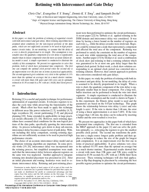
Retiming with Interconnect and Gate Delay Chris Chu∗,Evangeline F.Y.Young†,Dennis K.Y.Tong†,and Sampath Dechu‡∗Dept.of Electrical and Computer Engineering,Iowa State University,Ames,IA50011†Dept.of Computer Science and Engineering,The Chinese University of Hong Kong,Hong Kong ‡Physical Design Automation Group,Micron Technology,Inc.,Boise,ID83707AbstractIn this paper,we study the problem of retiming of sequential circuits with both interconnect and gate delay.Most retiming algorithms have assumed ideal conditions for the non-logical portions of the data paths,which are not sufficiently accurate to be used in high perfor-mance circuits today.In our modeling,we assume that the delay of a wire is directly proportional to its length.This assumption is rea-sonable since the quadratic component of a wire delay is significantly smaller than its linear component when the more accurate Elmore de-lay model is used.A simple experiment is conducted to illustrate the validity of this assumption.We present two approaches to solve this problem,both of which have polynomial time complexity.Thefirst one can compute the optimal clock period while the second one is an improvement over thefirst one in terms of practical applicability. The second approach gives solutions very close to the optimal(0.13% more than the optimal on average)but in a much shorter runtime.A circuit with more than22K gates and32K wires can be optimally retimed in83.56seconds by a PC with an1.8GHz Intel Xeon proces-sor.1IntroductionRetiming[1]is a useful and popular technique for performance optimization of sequential circuits.It relocates registers to re-duce the cycle time while preserving the functionality of the circuit.Much effort has been made to apply this technique in different areas like power reduction[2,3],testability[4,5], logic resynthesis[6],circuit partitioning[7–9]and physical planning[10].Some extended its applicability in large practi-cal circuits efficiently[11–18].However,most retiming algo-rithms have assumed ideal conditions for the non-logical por-tions of the data paths,specifically ignoring the interconnect delay.As process technology gets down to deep sub-micron, interconnect delay becomes a major factor of path delay.With-out including this delay component,existing retiming algo-rithms are not sufficiently accurate to be used in practical high performance circuits.The choice of an accurate interconnect delay model and an appropriate retiming algorithm are important.In some previ-ous works[19,20],interconnect delay was incorporated into the retiming process,but simplified assumptions were made such that the interconnect delay between adjacent registers on the same wire was neglected.Another approach to integrate retiming into detailed placement was presented in[21].After an initial placement and routing,heuristics were used to es-timate interconnect delay.Retiming and post-retiming place-ment were then performed to optimize the circuit performance.A recent paper[22]by Tabbara et al.applied retiming in the DSM domain and interconnect delay was considered.It was done by having a lower bound on the number of registers on each wire e uv,while the delays at nodes were irrelevant.Regis-ters could be retimed into a node that represented a component and affected the total area of the component.Retiming was performed to satisfy the constraint on the number of registers on each wire while minimizing the total area of the compo-nents.Another paper[13]by Deokar et ed a combination of clock skew and retiming tofind a retiming solution which was guaranteed to be at most one gate delay larger than the optimal clock period.In their work,a clock skew solution cor-responding to an optimal clock period was converted into a retiming solution.However,their current approach to perform this conversion considered only gate delays.In this paper,we study the problem of retiming with both in-terconnect and gate delay.In our modeling,the delay of a wire is assumed to be directly proportional to its length.When a wire is short,the quadratic component of the wire delay is sig-nificantly smaller than its linear component.For a long wire, buffer insertion can be performed to break the wire into short segments.A simple experiment is conducted to illustrate the validity of this assumption and the result is shown in Figure1. In this experiment,the Elmore delay model is used and the parameters are based on the0.07µm technology.This graph shows the relationship between wire delay(y-axis)and wire length(x-axis).If the wire is shorter than1.46mm,the error of using a linear approximation is at most5.48%.If the wire is longer than1.46mm,the delay can be reduced by inserting a buffer and the error resulted is even less.We present two approaches in this paper both of which have polynomial time complexity.Thefirst one is extended from the MILP approach in the paper[1]and can solve the prob-lem optimally,i.e.,relocating the registers to give the smallest possible clock period.The second one transforms the prob-lem into a single-source longest paths problem and then ap-plies a technique to reduce the size of the graph for longest path computation.It is an improvement over thefirst one in terms of practical applicability.It gives solutions very close to the optimal(0.13%more than the optimal on average)but in a much shorter runtime.Experimental results showed that a circuit with more than22K gates and32K wires could be retimed in83.56seconds by a PC with an1.8GHz Intel Xeon processor.These retiming techniques will alsofind applica-tions inflip-flop dropping in placement by estimating the best possible register positions to optimize the circuit performance.Permission to make digital or hard copies of all or part of this work for personal or classroom use is granted without fee provided that copies are n ot made or distributed for profit or commercial advan tage an d that copies bear this n otice an d the full citation on the first page. To copy otherwise, to republish, to post on servers or to redistribute to lists,No buffer One buffer Linear Approx.Delay (ps)Wire length (mm)5010015020025030035040045050055000.51.01.52.02.5Figure 1:A simple experiment to illustrate the relationship be-tween wire delay and wire length.The original placement solution will be modified to relocate the registers according to the retiming solution.However the effect will be minor if the original solution is not very densely placed.This is a reasonable assumption today as area is not a major concern while routability and congestion are the impor-tant factors for circuit performance.Register relocations can then be done by making use of the empty space or by shifting the placed cells a little bit.The remainder of this paper is organized as follows.We present the problem statement in Section 2.The optimal ap-proach and the fast approach are presented in Section 3and Section 4,respectively.Experimental results are shown and discussed in Section 5.A conclusion follows in Section 6.2Problem FormulationA sequential circuit can be represented by a directed graph G (V ,E ),where each node v corresponds to a combinational gate,and each directed edge e uv represents a connection from the output of gate u to the input of gate v ,through zero or more registers.Without loss of generality,we assume that G is strongly connected.If not,we can add a source node s and connect it to all primary inputs,add a target node t and connect all primary outputs to it,and connect t to s .Then the resulting graph is strongly connected.If we set the delay of s ,t and all the added edges to zero,and set the number of registers on e ts to one and that on the other added edges to zero,a retiming solution S of the modified graph will also be a valid retiming solution of the original graph as long as e ts still has one regis-ter in S .Let w uv be the number of registers of edge e uv .Let d uv be the interconnect delay of edge e uv if all the registers are removed.Note that the delay of an interconnect segment is as-sumed to be proportional to the length of the segment.Let d u be the gate delay of node u.Traditionally,interconnect delay is ignored during retiming.Figure 2:An example to illustrate the meaning of a (v ).A retiming solution can be viewed as a labeling of the nodes r :V →Z ,where Z is the set of integers [1].The retiming label r (v )for a node v represents the number of registers moved from its outputs toward its inputs.After retiming,the number ofregisters ˆw uv on an edge e uv is given by ˆwuv =r (v )+w uv −r (u ).As interconnect delay is dominating in the VDSM technol-ogy,the exact position of each register will affect the clock period.A retiming solution should specify both the retiming label r (v )for each node v and the exact positions of the ˆw uv registers on each edge e uv .Retiming should be formulated as a problem of determining a feasible retiming solution,i.e.,a solution in which the number of registers ˆw uv on each edge e uv is non-negative,such that the clock period of the retimed cir-cuit is minimized.In the following,we show how to check whether a particular clock period T can be achieved by a fea-sible retiming solution.The minimum achievable clock period T opt can then be found by binary search.3An Optimal ApproachThis approach is extended from the mixed integer linear pro-gramming (MILP)approach in [1].In the original formulation,only gate delay is considered and there is thus no difference be-tween having one or more than one registers on a wire.Their technique can be extended to solve the problem with both gate and interconnect delay optimally by modifying some of the constraint formulation.In order to formulate the problem as an MILP,for each gate v ,we need to define a term a (v )that represents the maximum arrival time at the output of gate v .An example to illustrate this definition is shown in Figure 2.We can then formulate the problem as the following MILP:d v ≤a (v )∀v ∈V (1)a (v )≤T ∀v ∈V(2)r (v )+w uv −r (u )≥0∀e uv ∈E(3)a (v )≥a (u )+d uv +d v −T (r (v )+w uv −r (u ))∀e uv ∈E(4)where T is the clock period that we want to check whether it is achievable.Since a (v )is the longest delay to the output of gate v from a register connected directly to an input of v ,this delay must be at least the delay of gate v ,so d v ≤a (v )as stated in (1).Besides,this delay cannot exceed the clock period T as required in (2).Constraint (3)is needed for a feasible retiming solution.Constraint (4)is to ensure that enough registers are on each edge e uv to achieve a clock cycle T .As the largest possible delay between two adjacent registers is T ,the right-hand side of constraint (4)is reduced by T for each register onedge e uv.Note that this constraint also captures the scenario when there is no registers on edge e uv.In that case,the arrival time at node u contributes directly to the arrival time at node v. By introducing a variable R(v)at each node v that is defined as a(v)/T+r(v),the above set of constraints(1)–(4)can be rewritten as a set of difference constraints as follows:R(v)−r(v)≥d vT∀v∈V(5)R(v)−r(v)≤1∀v∈V(6) r(u)−r(v)≤w uv∀e uv∈E(7)R(v)−R(u)≥d uvT+d vT−w uv∀e uv∈E(8)Notice that(5)–(8)is a set of difference constraints involving both integer and real variables.There are|V|real variables R(v),|V|integer variables r(v),and2|V|+2|E|constraints. This can be solved in polynomial time of O(|V||E|lg|V|+ |V|2lg2|V|)if Fibonacci heap is used as the data structure[23].If the above set of constraints is solvable,the values of r(v) and a(v)for all v∈V are known.We can thenfind the exact position of each register on a wire one by one as follows.For each edge e uv,if there are registers retimed on it,i.e.,r(v)+ w uv−r(u)>0,thefirst register on this edge will be placed at a distance of delay T−a(u)from the output of gate u.Other registers are then placed as far from each other as possible,i.e., at a distance of delay T from the previous one,until reaching the gate v.All the remaining registers on this edge are then placed right before v.4A Fast Near-Optimal ApproachIn this approach,wefirst replace each gate by a wire of the same delay and then solve the problem with only interconnect delay optimally and efficiently.Those registers retimed“into”a gate are moved either to the input or the output wires of the gate.The exact positions of the registers on the wires are then determined by a linear program to minimize the clock period. The solution obtained by this approach is very close to the op-timal on average as shown by the experimental results.In the following,wefirst show how the retiming problem with inter-connect delay only can be solved optimally.Then we describe in details how gate delay can be handled simultaneously.4.1Retiming with Interconnect Delay OnlyIn this subsection,we assume d v=0for all v∈V.Wefirst show that the clock period feasibility problem can be reduced to a single-source longest paths problem.We then present a fast algorithm to solve the longest paths problem.4.1.1Reduction to Single-Source Longest Paths Problem We solve the set of constraints(5)–(8)with the help of the fol-lowing lemma.Lemma1Given R(v)for all v∈V satisfying constraint(8), we can obtain a solution to constraints(5)–(8)by setting r(v)= R(v) for all v∈V.Proof:It is clear that0≤R(v)− R(v) <1for all v∈V. Therefore,(5)and(6)are satisfied.For any e uv∈E, r(u)−r(v)≤R(u)−r(v)as r(u)≤R(u)≤(d uvT+R(u))−r(v)as d uvT>0≤(w uv+R(v))−r(v)by constraint(8)<w uv+1as R(v)−r(v)<1As r(u)−r(v)is an integer,it must be less than or equal to w uv.Hence,constraint(7)is also satisfied.2 Lemma1implies that we canfirst solve constraint(8)tofind R(v)and it is then easy tofind r(v)to satisfy the other three constraints.Notice that if d v=0for some v∈V,Lemma1 does not hold as constraint(5)is not satisfied.In other words, this idea cannot be applied to the retiming problem with both interconnect and gate delay discussed in Section3.The problem offinding R(v)for all v∈V to satisfy con-straint(8)can be viewed as a single-source longest paths prob-lem on G with length l uv equals d uv/T−w uv for each e uv∈E. As G is strongly connected,we can pick an arbitrary node as the source node s.1Note that edge lengths can be positive.If G has a positive cycle,the set of constraints has no solutions. It means that the clock period T is infeasible.The solution to this problem is presented in the following subsection.4.1.2Fast Single-Source Longest Paths AlgorithmThe single-source longest paths problem in Section4.1.1can be solved by the Bellman-Ford algorithm[24].The time com-plexity is O(|V||E|),which is at least a factor ofΘ(lg|V|)faster than the optimal algorithm in Section3.In practice,it is a fac-tor ofΘ(lg2|V|)faster as|E|=O(|V|).However,this algo-rithm may still be slow in practice.In this section,we present a single-source longest paths algorithm which is faster in prac-tice.The basic idea is to reduce the size of G by compacting some paths into edges before the Bellman-Ford algorithm is applied.The details are given below.Wefirst transform the graph G(V,E)into a directed acyclic graph(DAG)G (V ,E )by performing a depth-first traver-sal[24]starting from the source node s.The depth-first traver-sal defines a tree in G.Those non-tree edges running from a node u to an ancestor v of u are called back edges.If we point all incoming back edges of a node v to an extra node v ,the resulting graph will be a DAG because every simple cycle in G involves exactly one back edge.Formally,we use E b to denote the set of back edges and V b to denote the set of nodes with an incoming back edge.For each node v in V b,we introduce an extra node v .The back edge e uv is removed from the graph and the edge e uv is added.The resulting DAG is G (V ,E )where V =V∪{v |v∈V b}and E =(E−E b)∪{e u,v |e u,v∈E b}. We set the length l uv of the edge e uv to l uv.To illustrate the transformation,consider the graph G in Figure3(a)with source node A.Suppose the depth-first traversal visits the nodes in the order ACDEFB.Then E b={e DA,e CA,e FC,e FA} and V b={A,C}.We introduce two extra nodes A and C ,and replace the four edges e CA,e DA,e FA and e FC with the edges 1If the original circuit is not strongly connected,a source node s has already been added.Depth first traversalfrom node A(a) Original graph G(b) Directed acyclic graph G’Figure3:An example to illustrate the transformation to a DAG.e CA ,e DA ,e FA and e FC ,respectively.The resulting DAG isshown in Figure3(b).We then construct a graph H with node set V b.The edge setE H contains an edge e uv for u,v∈V b if there exists a path in Gwith either no back edge or one back edge at the end from uto v.The length l H uv of the edge e uv is the longest path distanceamong those paths.Note that the longest path distance in Gwith no back edge(respectively,with one back edge at the endof the path)from u to v equals the longest path distance inG from u to v(respectively,from u to v ).Hence l H uv for allu,v∈V b can be computed by solving|V b|single-source longestpaths problems in G for different source nodes in V b.As G is aDAG,each single-source longest paths problem can be solvedin linear time by visiting the nodes in topological order.Thetime complexity to construct H is therefore O(|V b||E|).It is obvious that every path in H corresponds to at least onepath in G of the same length.Therefore if H contains a positivecycle,G will also contain a positive cycle.On the other hand,if G contains a positive cycle,the cycle can be broken up into aset of paths p1,p2,...,p k such that both endpoints of each pathp i are in V b.Notice that each path p i corresponds to an edge inH of at least the same length.So H must also contain a posi-tive cycle.Therefore we can solve the positive cycle detectionproblem in H instead of in G.If H has no positive cycles,R(v)for all v∈V b can be found from H.R(v)for all v∈V−V b canthen be found in linear time by propagating R(v)for all v∈V bthrough G in topological order.4.1.3The Retiming Algorithm and Time ComplexityThe complete retiming algorithm I-Retiming()is summarizedbelow.The most time consuming steps are step7and step8inside the binary search loop.Step7can be done in O(|V b||E|)time as discussed above.Step8can be done in O(|V b||E H|)time by the Bellman-Ford algorithm.As V b contains muchfewer nodes than V and E H usually contains comparable orfewer edges than E,this technique is usually much more effi-cient than applying the Bellman-Ford algorithm to G directly.The total time complexity is O(|V b|max{|E|,|E H|}lg KεTopt),whereεis the error bound for the binary search,K is the differ-ence between the upper and lower bounds of the clockperiod(a) Original graph G(b) Transformed graph G~Figure4:Representation of gates by wires.initially,and T opt is the optimal clock period.Algorithm I-Retiming()Input:A sequential circuit C with interconnect delay onlyOutput:An optimally retimed circuit of C1.Build graph G(V,E)from C2.Build DAG G by DFS(G)3.C up=a feasible clock,C low=an infeasible clock4.Do5.T=(C up+C low)/26.Update edge lengths of G according to T7.Build graph H(V b,E H)with E H={e uv|u∈anc(v)∪anc(v )}byfinding single-source longest paths in G8.If H does not have any positive cycle then9.C up=T10.Else11.C low=T12.while(C up−C low)/C up>ε13.T=C up//C up is always a feasible clock periodpute R(v)and r(v)for each node v∈Vpute the exact position of each register on a wire4.2Retiming with Interconnect and Gate DelayIn this section,we discuss how to consider interconnect andgate delay simultaneously based on the above algorithm forinterconnect delay only.To consider gate delay,wefirst repre-sent a gate v with delay d v by a wire e v1v2with delay d v1v2=d v.This transformation for the circuit in Figure3(a)is shown inFigure4(b).We can then obtain an optimal retiming on thistransformed circuit˜G using the algorithm in Section4.1.How-ever the retiming solution obtained on˜G may not be feasiblefor the original circuit G because some registers may be re-timed into a wire that represents a gate.Therefore,we need toperform a post-processing step to get back a feasible retimingsolution for G from the optimal retiming solution for˜G.Thisis done by linear programming.First of all,we move the registers in a gate either backwardto the input wires or forward to the output wires of the gate,depending on which direction has a shorter distance.An ex-ample showing the relocation of registers is given in Figure5.After this relocation step,the number of registersˆw uv on eachedge e uv isfixed.A linear program is used to determine the(a) A retimed solution in G~(b) Registers are relocated in G Figure5:Relocation of registers retimed into a gate.exact positions of the registers on the edges.The objective of the linear program is to minimize the clock period T subject to the constraints in register count on each edge.In the fol-lowing,we use x k uv to denote the delay from the k th register to the k+1st register of the wire from node u to node v in G for k=0,1,...,ˆw uv.Notice that whenˆw uv=0,x0uv is the delay of the whole wire,and when k=0and k=ˆw uv>0,x k uv are the delays of the wire from node u to thefirst register and from the last register to node v,respectively.The linear program is formulated as follows:Minimize TSubject to∑ˆw uvk=0x k uv=d uv∀e uv∈E(A)xˆw uv uv+d v≤a(v)∀e uv∈E s.t.ˆw uv>0(B)a(u)+x0uv≤T∀e uv∈E s.t.ˆw uv>0(C)a(u)+d uv≤a(v)∀e uv∈E s.t.ˆw uv=0(D) For the circuit in Figure5(b),example constraints are x0CD+ x1CD=d CD for type(A),x1CD+d D≤a(D)for type(B),a(C)+ x0CD≤T for type(C),and a(B)+d BD≤a(D)for type(D). We can solve this linear program to obtain the best possible clock period T∗under the register count constraint on each edge.The overall algorithm IG-Retiming()to handle both in-terconnect and gate delay is summarized as follows: Algorithm IG-Retiming()Input:A sequential circuit C with both interconnect and gate delay Output:A retimed circuit of C1.Build graph G from C2.Build˜G by replacing each gate in G by a wire of the same delay3.Solve the retiming problem of˜G by I-Retiming()4.Move registers away from wires that represent gates5.Set up a linear program based on the register count on each edge6.Solve the linear program to obtain a feasible retiming solutionand the smallest possible clock period T∗5Experimental ResultsWe implemented the two approaches in a1.8GHz Intel Xeon PC with512KB cache and512MB RAM.We tested them with circuits from the ISCAS89benchmark suite.In our ex-periments,we implement the circuits in a0.25µm process.We layout the circuits by Silicon Ensemble.Wire delays are then extracted according to the layout.In our current implementa-tion,the lower and upper bounds of the binary search are setto0and100ns respectively.In the near-optimal approach,weperform the procedure I-Retiming()with an error bound of1%.After assigning the registers retimed into a gate to the appro-priate wires,a linear program is set up to relocate the registerson the wires to get the smallest possible clock period T∗.Inthe optimal approach,binary search is performed until an errorbound of0.01%is obtained.We call the resulting clock periodT opt.Notice that we do not need to obtain a very accurate re-sult from I-Retiming()because the solution is optimized by thelinear program afterwards.On average,the number of binarysearch iterations is9.6for the near-optimal approach and16.5for the optimal approach.The results are shown in Table1.The second and thirdcolumns give the number of nodes and the number of edgesin the graph G,respectively.Notice that all circuits are notstrongly connected.The number of nodes and edges listed arethose after the addition of the source node,the target node,andthe associated edges.The fourth andfifth columns show thenumber of nodes and the number of edges in the reduced graphH,respectively.These two values are dependent on the node chosen as the root in the depth-first traversal.In our current im-plementation,we always pick the additional node s as the root.We notice that using other nodes as the root does not changethe result significantly.The speedup of the Bellman-Ford al-gorithm by the graph reduction approach in Section4.1.2is (|V||E|)/(|V b||E H|),which is given in the sixth column.The graph reduction approach is faster in all circuits except s38584.On average,it is faster by30.61times.However,the speedupis less(may even be less than one)for larger circuits.The rea-son is that|E H|is roughly quadratic in|V b|.For the circuits in Table1,the ratio of|E H|to|V b|2is from0.11to0.86with an average of0.41.Therefore,the graph reduction approach may not be useful for large circuits.We can avoid a slowdown of the Bellman-Ford algorithm by determining whether to use G or H based on the ratio(|V||E|)/(|V b||E H|).|V b|and|E H|can be found in O(|V b||E|)time.Moreover,we only need to per-form this checking once for each circuit.Hence,the runtime overhead is insignificant compared with the total runtime. The seventh,eighth,and ninth columns show the runtime of the I-Retiming()procedure,the time taken to solve the linear program,and the total runtime,respectively.The tenth col-umn shows the runtime for the optimal approach.We can see that the near-optimal approach is much more efficient than the optimal approach(especially for large circuits).The eleventh and twelfth columns show the clock period T∗and T opt ob-tained by the near-optimal approach and the optimal approach, respectively.The last column is the percentage increase of T∗over T opt.The clock period produced by the near-optimal ap-proach is only0.13%more than that by the optimal approach on average.The optimal clock period is found in seven out of thirteen circuits.6ConclusionWe have presented two elegant approaches to perform retim-ing on sequential circuits with both interconnect and gate de-lay.This is a pioneer work in solving this problem as far as weNo.of No.of No.of No.of CPU Time Clock Period Circuit Nodes Edges Nodes Edges|V||E|I-Retiming+LP=IG-Retiming Optimal T∗T opt T∗−T optT opt in V in E in V b in E H|V b||E H|(sec)(sec)(sec)(sec)(ns)(ns)(%) s148865514052762754.360.090.190.28 5.6218.8518.820.16 s149464914113074940.750.090.160.25 4.3720.7820.780.00 s327115742707112336011.320.380.71 1.0933.7010.2410.240.00 s33301791289056120077.020.130.370.5043.1427.0527.050.00 s33841687278298204123.460.160.580.7425.1924.2124.160.21 s48632344409315420413 3.05 2.130.99 3.1287.7523.5823.580.00 s53782781426166255470.300.550.61 1.16138.6827.2727.250.07 s666930825399671876132.380.36 1.55 1.91177.5923.0722.96 1.00 s92345599800532526570 5.19 2.69 1.39 4.08512.8642.7342.730.00 s1320779531130255044825 3.65 6.45 1.668.111161.0772.3472.340.00 s15850977413794603100738 2.2221.42 2.6024.021545.5967.8267.820.00 s359321606728590884163945 3.1754.59 6.6661.258644.2729.5929.540.17 s3841722181321351657308790 1.3972.6410.9283.567680.7936.5336.520.03 s385841925533010192411158680.30433.8211.81445.63>1500094.26Table1:The runtime of the algorithms and the clock periods obtained.know.Most traditional retiming algorithms have neglected in-terconnect delay.Ourfirst approach is extended from the MILP approach in the paper[1]and can solve the problem optimally. Our second approach is an improvement over thefirst one in terms of practical applicability.The main idea is to transform the problem into a single-source longest paths problem in a reduced graph.We have implemented both algorithms,and compared their performance on ISCAS89benchmark circuits. Experimental results show that the second approach gives so-lutions that are only0.13%larger than the optimal on average but in a much shorter runtime.References[1]Charles E.Leiserson and James B.Saxe.Retiming SynchronousCircuitry.Algorithmica,6:5–35,1991.[2] C.V.Schimpfle,Sven Simon,and Josef A.Nossek.OptimalPlacement of Registers in Data Paths for Low Power Design.In Proc.ISCAS,pages2160–2163,1997.[3]J.Monteiro,S.Devadas,and A.Ghosh.Retiming SequentialCircuits for Low Power.In Proc.ICCAD,pages398–402,1993.[4] A.El-Maleh,T.E.Marchok,J.Rajski,and W.Maly.Behaviorand Testability Preservation under the Retiming Transformation.IEEE TCAD,16:528–542,1997.[5]S.Dey and S.Chakradhar.Retiming Sequential Circuits to En-hance Testability.In Proc.IEEE VLSI Test Symposium,pages 28–33,1994.[6]Rajeev K.Ranjan,Vigyan Singhal,Fabio Somenzi,andRobert K.Brayton.On the Optimization Power of Retiming and Resynthesis Transformation.In Proc.ICCAD,pages402–407, 1998.[7]Peichen Pan,Arvind K.Karandikar,and C.L.Liu.OptimalClock Period Clustering for Sequential Circuits with Retiming.IEEE TCAD,17(6):489–498,1998.[8]Jason Cong,Honching Li,and Chang Wu.Simultaneous Cir-cuit Partitioning/Clustering with Retiming for Performance Op-timization.In Proc.DAC,pages460–465,1999.[9]Jason Cong,Sung Kyu Lim,and Chang Wu.PerformanceDriven Multi-level and Multiway Partitioning with Retiming.In Proc.DAC,pages274–279,2000.[10]Jason Cong and Sung Kyu Lim.Physical Planning with Retim-ing.In Proc.ICCAD,pages2–7,2000.[11]N.Shenoy and R.Rudell.Efficient Implementation of Retiming.In Proc.ICCAD,pages226–233,1994.[12]N.Shenoy,R.K.Brayton,and A.Sangiovanni-Vincentelli.Re-timing of Circuits with Single Phase Transparent Latches.In Proc.ICCAD,pages86–89,1991.[13]Rahul B.Deokar and Sachin S.Sapatnekar.A Fresh Look atRetiming via Clock Skew Optimization.In Proc.DAC,pages 310–315,1995.[14]Marios C.Papaefthymiou.Asymptotically Efficient Retimingunder Setup and Hold Constraints.In Proc.ICCAD,pages396–401,1998.[15]H.J.Touati and puting the Initial States ofRetimed Circuits.IEEE TCAD,12:157–162,1993.[16]I.Karkowski and R.H.J.M.Otten.Retiming Synchronous Cir-cuitry with Imprecise Delay.In Proc.DAC,pages322–326, 1995.[17]Vigyan Singhal,Sharad Malik,and Robert K.Brayton.TheCase for Retiming with Explicit Reset Circuitry.In Proc.IC-CAD,pages618–625,1996.[18]N.Maheshwari and S.S.Sapatnekar.An Improved Algorithmfor Minimum-area Retiming.In Proc.DAC,pages2–7,1997.[19]T.Soyata and E.G.Friedmann.Retiming with nonzero clockskew,variable register and interconnect delay.In Proc.ICCAD, pages234–241,1994.[20]Kumar lgudi and Marios C.Papaefthymiou.DELAY:AnEfficient Tool for Retiming with Realistic Delay Modeling.In Proc.DAC,pages304–309,1995.[21]Tzu-Chieh Tien,Hsiao-Pin Su,and Yu-Wen Tsay.IntegratingLogic Retiming and Register Placement.In Proc.ICCAD,pages 136–139,1998.[22]Abdallah Tabbara,Robert K.Brayton,and A.Richard Newton.Retiming for DSM with Area-Delay Trade-offs and Delay Con-straints.In Proc.DAC,pages725–730,1999.[23] C.E.Leiserson and James B.Saxe.A Mixed-Integer Program-ming Problem Which is Efficiently Solvable.Journal of Algo-rithms,9:114–128,1988.[24]Thomas H.Cormen and Charles E.Leiserson and Ronald L.Rivest.Introduction to Algorithms.McGraw Hill,eighth edi-tion,1992.。


doi:10.3969/j.issn.1003-3114.2024.01.006引用格式:刘军,王靖思,宋瑞良,等.基于共振隧穿二极管的太赫兹技术研究进展[J].无线电通信技术,2024,50(1):58-66.[LIU Jun,WANG Jingsi,SONG Ruiliang,et al.Recent Progress of Terahertz Technology Based on Resonant Tunneling Diode [J].Radio Communications Technology,2024,50(1):58-66.]基于共振隧穿二极管的太赫兹技术研究进展刘㊀军1,王靖思2,宋瑞良1,刘博文1,刘㊀宁1(1.中国电子科技集团公司第五十四研究所北京研发中心,北京100041;2.北京跟踪与通信技术研究所,北京100094)摘㊀要:共振隧穿二极管(Resonant Tunneling Diode,RTD)是一种基于量子隧穿效应的半导体器件,同时具有非线性特性和负阻特性,通过改变偏置电压可以作为太赫兹源和太赫兹探测器,在未来6G 技术中通信感知一体化方面具有优势㊂简要总结了基于RTD 实现的器件的工作原理,对基于RTD 实现的太赫兹源和太赫兹探测器㊁太赫兹通信系统以及太赫兹雷达系统等太赫兹技术的研究进展进行介绍,并对当前存在的技术挑战和未来的发展方向进行探讨㊂基于RTD 的太赫兹技术凭借其突出的优势,将成为未来电子器件领域重要的发展方向㊂关键词:共振隧穿二极管;太赫兹源;太赫兹通信;太赫兹探测器中图分类号:TN919.23㊀㊀㊀文献标志码:A㊀㊀㊀开放科学(资源服务)标识码(OSID):文章编号:1003-3114(2024)01-0058-09Recent Progress of Terahertz Technology Based onResonant Tunneling DiodeLIU Jun 1,WANG Jingsi 2,SONG Ruiliang 1,LIU Bowen 1,LIU Ning 1(1.Beijing Research and Development Center,The 54th Research Institute of CETC,Beijing 100041,China;2.Beijing Institute of Tracking and Telecommunication Technology,Beijing 100094,China)Abstract :Resonant Tunneling Diode (RTD)that has both nonlinear and negative resistance characteristics is a semiconductor de-vice based on the quantum tunneling effect.Advantages of RTD include the facts that they can operate both as an oscillator and detector by changing the bias voltage and show advantages in the integration of communication and sensing for 6G.This paper introduces work-ing principles of RTD and the research progress of terahertz technology based on RTD from the aspects of terahertz sources,terahertz detectors,terahertz communication system and terahertz radar system,and discusses about current technological challenges and future perspectives.RTD-based terahertz technology will become an important development direction in the field of electronic devices in thefuture due to its outstanding advantages.Keywords :RTD;terahertz sources;terahertz communication;terahertz detectors收稿日期:2023-09-22基金项目:国家重点研发计划(2023YFE0206600)Foundation Item :NationalKeyR&DProgramofChina(2023YFE0206600)0 引言在移动通信技术从1G 发展到5G 的过程中,逐步实现了从语音㊁数字消息业务㊁移动互联网㊁智能家居㊁远程医疗㊁智能物联和虚拟现实等应用的发展[1]㊂6G 技术作为5G 技术的演进,不仅作为高速通信系统,也将作为高灵敏度探测系统,以更好地感知物理环境,获得高精度定位㊁成像以及环境重建等信息㊂太赫兹波介于微波与红外之间,具有波束窄㊁带宽宽㊁穿透性高㊁能量性低等特点,易于实现无线通信与无线感知功能的单片集成,从而实现感知功能与通信功能的相互促进与增强,进一步实现万物 智联 [2-4]㊂太赫兹波的产生和探测技术,是太赫兹应用系统的核心技术[5-6]㊂基于固态电子学方法的常温太赫兹源有碰撞电离雪崩渡越时间二极管(Impact Avalanche and Transist Time Diode,IMPATT)[7]㊁耿式二极管[8-9]㊁肖特基势垒二极管(Schottky BarrierDiode,SBD)[10]、超晶格电子器件[11]、晶体管[12]和共振隧穿二极管(ResonantTunnelingDiode,RTD)[13]。

第43卷㊀第1期2022年1月发㊀光㊀学㊀报CHINESE JOURNAL OF LUMINESCENCEVol.43No.1Jan.,2022㊀㊀收稿日期:2021-10-25;修订日期:2021-11-11㊀㊀基金项目:国家重点研发计划(2017YFB0404104);国家自然科学基金(61974139);北京自然科学基金(4182063)资助项目Supported by National Key R&D Program of China (2017YFB0404104);National Natural Science Foundation of China (61974139);Beijing Natural Science Foundation(4182063)文章编号:1000-7032(2022)01-0001-07量子垒高度对深紫外LED 调制带宽的影响郭㊀亮1,2,郭亚楠1,2,羊建坤1,2,闫建昌1,2,王军喜1,2,魏同波1,2∗(1.中国科学院半导体研究所半导体照明研发中心,北京㊀100083;2.中国科学院大学材料与光电研究中心,北京㊀100049)摘要:AlGaN 基深紫外LED 由于具有高调制带宽和小芯片尺寸,在紫外光通信领域受到越来越多的关注㊂本研究通过改变生长AlGaN 量子垒层的Al 源流量,生长了三种具有不同量子垒高度的深紫外LED,研究了量子垒高度对深紫外LED 光电特性和调制特性的影响㊂研究发现,随着量子垒高度的增加,深紫外LED 的光功率出现先增加后减小的趋势,量子垒中Al 组分为55%的深紫外LED 的光功率相比50%和60%的深紫外LED 提升了近一倍㊂载流子寿命则出现先减小后增大的趋势,且发光峰峰值波长逐渐蓝移㊂APSYS 模拟表明,随着量子垒高度增加,量子垒对载流子的束缚能力增强,电子空穴波函数空间重叠增加,载流子浓度和辐射复合速率增加;但进一步增加量子垒高度又会由于电子泄露,空穴浓度降低,从而辐射复合速率降低㊂量子垒中Al 组分为55%的深紫外LED 的-3dB 带宽达到94.4MHz,高于量子垒Al 组分为50%和60%的深紫外LED㊂关㊀键㊀词:紫外光通信;深紫外发光二极管;多量子阱层;调制带宽;发光功率中图分类号:TN383+.1;TN929.12㊀㊀㊀文献标识码:A㊀㊀㊀DOI :10.37188/CJL.20210331Effect of Barrier Height on Modulation Characteristics ofAlGaN-based Deep Ultraviolet Light-emitting DiodesGUO Liang 1,2,GUO Ya-nan 1,2,YANG Jian-kun 1,2,YAN Jian-chang 1,2,WANG Jun-xi 1,2,WEI Tong-bo 1,2∗(1.Research and Development Center for Semiconductor Lighting Technology ,Institute of Semiconductors ,Chinese Academy of Sciences ,Beijing 100083,China ;2.Center of Materials Science and Optoelectronics Engineering ,University of Chinese Academy of Sciences ,Beijing 100049,China )∗Corresponding Author ,E-mail :tbwei @Abstract :AlGaN-based deep ultraviolet LED has attracted more and more attention in ultravioletcommunication due to its high modulation bandwidth and small chip size.In this study,AlGaN-based deep ultraviolet LEDs with varied Al composition of 50%,55%,60%in quantum barriers are fabricated.The effect of barrier height on the photoelectric and modulation characteristics of deep ultraviolet LEDs is studied.It is found that the optical power and external quantum efficiency (EQE)of the deep ultraviolet LED increase first and then decreased,and carrier lifetime decreases first and then increases as the quantum barrier height increases.The peak wavelength of the spectra shows a blue-shift.APSYS simulation revealed that the spacial overlap between the wave function of electron and hole is enhanced as Al composition increases.But further increase on barrier height will lead to current leakage which reduces the radiation recombination rate and carrier density in . All Rights Reserved.2㊀发㊀㊀光㊀㊀学㊀㊀报第43卷quantum well layer.The-3dB bandwidth of deep ultraviolet LED with55%Al composition inquantum barrier is measured to be94.4MHz,higher than those with50%and60%Al composition in quantum barrier.Key words:ultraviolet communication;deep ultraviolet light-emitting diodes;multiple-quantum-well layer;modula-tion bandwidth;optical power1㊀引㊀㊀言随着深紫外LED和日盲探测器的发展,紫外光通信受到越来越多的关注㊂紫外光通信利用紫外光传输信号,该信号可以被漂浮在空气中的微粒和气溶胶等散射和反射,实现非视距通信[1-2]㊂紫外光通信中使用的紫外光也称为日盲紫外光,它在光谱中位于200~280nm之间[3-4]㊂当太阳辐射穿过大气层时,会被空气中的水蒸气㊁二氧化碳㊁氧气㊁臭氧㊁悬浮颗粒和其他气体分子强烈散射㊁吸收或反射,从而导致太阳光谱不连续㊂在所有分子和粒子中,仅占大气0.01%~0.1%的臭氧在紫外光谱中具有很强的吸收带,从而使得到达地表的太阳光中日盲紫外光含量极少,这则为紫外光通信提供了低背景噪声的通信环境[5]㊂同时,紫外光通信还具有高保密性㊁无需频段许可㊁抗干扰能力强等优势,这使得紫外光通信在军事领域具有重要应用价值㊂紫外光源作为紫外光通信系统中重要的组成部分,其光功率决定了紫外光通信系统的传输距离,而其带宽决定了通信速率的上限[6]㊂紫外光通信系统中最常用的三种光源包括气体放电灯㊁激光器和LED㊂气体放电灯制造成本低㊁输出功率大,激光器的光线相干性高㊁单色性好㊁发散性低,然而这两种光源都存在体积大㊁功耗大㊁调制速率低的缺点㊂AlGaN基LED由于具有更高的调制带宽和更小的芯片尺寸,在紫外光通信中得到了越来越广泛的应用[7-9]㊂近年来,越来越多的研究团体开始研究基于深紫外LED作为光源的紫外光通信㊂Alkhazragi等基于商用发光波长为279nm的深紫外LED实现了1m链路上通信速率为2.4Gbps的紫外光通信系统,测得调制带宽为170MHz[10]㊂2018年,Kojima等基于调制带宽为153MHz㊁发光波长为280nm的深紫外LED,在1.5m链路上实现了1.6Gbps的通信速率[11]㊂2019年,He等制备了AlGaN基262nm深紫外Micro-LED阵列,在71 A/cm2电流密度下,测得调制带宽达到了438 MHz,在0.3m链路上实现了高达1.1Gbps的数据传输速率[12]㊂Zhu等制备了100μm深紫外Micro-LED,在400A/cm2电流密度下,测得调制带宽为452.53MHz[13]㊂尽管AlGaN基深紫外LED在紫外光通信中已经得到了广泛应用,但目前大部分研究仍集中在LED芯片工艺的改进上㊂关于深紫外LED外延结构对调制特性的影响的研究几乎处于空白状态㊂本研究通过改变生长AlGaN量子垒层时的Al源流量,控制了量子垒中Al组分分别为50%㊁55%和60%,生长了三种具有不同量子垒高度的深紫外LED,研究了量子垒高度对深紫外LED光电特性和调制特性的影响㊂并借助APSYS模拟和时间分辨光致发光光谱对实验结果进行了深入分析㊂2㊀实㊀㊀验2.1㊀样品制备实验中首先在c面蓝宝石衬底上生长1μm 厚的AlN缓冲层,然后在1130ħ下沉积20个周期的AlN(2nm)/Al0.6Ga0.4N(2nm)超晶格层㊂然后依次生长1.8μm厚Si掺杂浓度为3ˑ1018 cm-3的n-Al0.61Ga0.39N层,5个周期Al0.4Ga0.6N图1㊀紫外外延片结构示意图Fig.1㊀Wafer structure of ultraviolet LED. All Rights Reserved.㊀第1期郭㊀亮,等:量子垒高度对深紫外LED调制带宽的影响3㊀(3nm)/Al0.5/0.55/0.6Ga0.5/0.45/0.4N(12nm)多量子阱层,50nm厚的Mg掺杂p-Al0.6Ga0.4N电子阻挡层,30nm厚p-Al0.5Ga0.5N层以及150nm厚Mg 掺杂浓度为1ˑ1018cm-3的p-GaN层㊂随后,在800ħ氮气气氛下退火20min以激活Mg受主㊂对生长得到的深紫外LED外延片使用标准紫外流片工艺,制备了倒装结构深紫外LED,芯片尺寸为250μmˑ550μm,图1为外延片结构示意图㊂2.2㊀样品表征LED光功率测试采用的是远方光电公司HAAS-2000高精度快速光谱辐射计,该设备光谱范围为200~2550nm㊂光致发光光谱测试采用215nm紫外激光器作为激发光源,激光功率为31 mW,所用光栅线密度为1200l/mm,测试波长范围为240~320nm,步长为0.2nm,积分时间为1.0s,测试环境温度为295K㊂带宽测试系统采用安捷伦E5061B型网络分析仪,其扫描频率范围为5Hz~3GHz,可覆盖氮化物LED的频率响应范围㊂直流偏置源采用Keithley2420作为电流源,该电流源最大输出电流为3A,最大输出电压为60 V㊂紫外探测器采用Thorlabs公司APD430A2/M 型硅基雪崩探测器,可探测波长范围是200~ 1000nm,可覆盖整个UVC波段㊂图2为实验中使用的带宽测试系统示意图㊂图2㊀带宽测试系统示意图Fig.2㊀Diagram of bandwidth testing system3㊀结果与讨论3.1㊀电致发光光谱图3是3种不同量子垒高度深紫外LED的EL测试结果㊂在20mA电流下,量子垒中Al组分为50%㊁55%和60%的深紫外LED的峰值波长分别为280.4,276.5,274.0nm,可以看出随着量子垒中Al组分的增加,深紫外LED的峰值波长逐渐蓝移㊂这是因为随着量子垒高度增加,量子阱对电子空穴的束缚能力增加,电子和空穴波函数的空间分离减小,量子限制效应增强,从而导致蓝移㊂同时可以看出,随着电流从20mA增加到100mA,深紫外LED的峰值波长逐渐红移㊂Al组分为50%的深紫外LED的峰值波长红移了1.2nm,Al组分为55%的深紫外LED的峰值波长红移了2nm,Al组分为60%的深紫外LED的峰值波长红移了1nm㊂同时LED的发光峰半高宽也逐渐展宽,Al组分为50%的深紫外LED的半高宽从9.9nm展宽到10.8nm,Al组分为55%的深紫外LED的半高宽从11.3nm展宽到12nm, Al组分为60%的深紫外LED的半高宽从10.7nm图3㊀量子垒中Al组分为50%(a)㊁55%(b)㊁60%(c)的深紫外LED的EL光谱随电流的变化㊂Fig.3㊀EL spectra of ultraviolet LED with Al composition of 50%(a),55%(b),60%(c)in quantum barrierunder varied currents.. All Rights Reserved.4㊀发㊀㊀光㊀㊀学㊀㊀报第43卷展宽到11.7nm㊂这是因为根据焦耳定律,随着电流增加,单位时间内产生的热量增加㊂根据能带宽度和温度的关系,深紫外LED的能带宽度会随着温度升高而线性减小,从而导致发光波长红移[14]㊂热量的增加还会导致量子限制斯塔克效应增强,从而导致半高宽增加[15]㊂3.2㊀光功率对3种不同量子垒高度的深紫外LED芯片进行光电测试,得到不同测试电流下的光功率测试结果,如图4所示㊂可以看出光功率随着量子图4㊀量子垒中Al组分为50%㊁55%㊁60%的深紫外LED 的光功率随电流的变化㊂Fig.4㊀Optical power of ultraviolet LED with Al composition of50%,55%,60%in quantum barrier under var-ied currents.垒高度的增加,出现先增大后减小的趋势㊂这是因为随着量子垒高度的增加,量子阱对电子空穴的束缚能力增强,使得电子空穴浓度增加,从而导致光功率增大㊂但进一步增加量子垒高度,会导致电子阻挡层对过冲电子的束缚能力减弱,过冲电子与p型区的空穴复合,导致空穴电流减小,最终导致光功率降低[16]㊂3.3㊀APSYS模拟我们使用APSYS软件对不同量子垒高度的AlGaN基深紫外LED的能带结构进行了模拟㊂模拟时,深紫外LED的注入电流为62.5mA,器件尺寸为250μmˑ250μm,从下到上为蓝宝石衬底㊁AlN缓冲层㊁n-Al0.55Ga0.45N层㊁有源区㊁p-Al0.65Ga0.35N电子阻挡层㊁p-Al0.55Ga0.45N层㊁p-GaN层㊂有源区由5个量子阱层和6个量子垒层组成,阱层为2nm厚的Al0.45Ga0.55N,垒层为10nm厚的Al0.5/0.55/0.6Ga0.5/0.45/0.4N㊂不同量子垒高度的AlGaN基的深紫外LED的能带结构如图5(a)㊁(b)㊁(c)所示㊂可以看出,随着量子垒高度的增加,电子和空穴的波函数空间分离逐渐减小,我们进一步对其辐射复合速率进行了模拟,模拟结果如图5(d)所示㊂辐射复合速率随着量子垒高度出现了先增加后减小的趋势㊂这是因为随着量子垒高度的增加,量子垒对载流子的束缚作图5㊀量子垒中Al组分为50%(a)㊁55%(b)㊁60%(c)的深紫外LED的能带结构示意图;(d)量子垒中Al组分为50%㊁55%和60%的深紫外LED的辐射复合速率分布示意图㊂Fig.5㊀Band structure of ultraviolet LED with Al composition of50%(a),55%(b),60%(c)in quantum barrier.(d)Ra-diation recombination rate of ultraviolet LED with Al composition of50%,55%and60%in quantum barrier.. All Rights Reserved.㊀第1期郭㊀亮,等:量子垒高度对深紫外LED调制带宽的影响5㊀用增加,使得量子阱内的载流子浓度增大,同时由于电子和空穴的空间波函数重叠增加,辐射复合所占的比重也会增加,从而辐射复合速率增大㊂但进一步增加量子垒高度又会由于电子泄漏,从而导致辐射复合速率减小[17-18]㊂3.4㊀时间分辨光致发光光谱我们对不同量子垒高度的深紫外LED进行了时间分辨光致发光光谱(TRPL)测试㊂不同量子垒高度深紫外LED的TRPL测试结果如图6所示㊂通过对曲线的衰减部分使用以下公式进行双衰减指数拟合[19]:I(t)=A1e-ττ1+A2e-ττ2,(1)其中τ1满足1/τ1=1/τnr+1/τ2,τnr为非辐射复合载流子寿命,τ2为辐射复合载流子寿命㊂量子垒中Al组分为50%㊁55%和60%的深紫外LED的载流子寿命分别为432,276,352ps㊂可以看出载流子寿命随着量子垒中Al组分的增加出现先减小后增大的趋势㊂图6㊀量子垒中Al组分为50%㊁55%㊁60%的深紫外LED的TRPL光谱随电流的变化㊂Fig.6㊀TRPL spectra of ultraviolet LED with Al composition of50%,55%,60%in quantum barrier.热平衡状态下,pn结中的载流子复合速率可以由以下公式得到:R=B(N0+Δn)(P0+Δn)-BN0P0,(2)其中B为复合常数,N0为电子浓度,P0为空穴浓度,Δn为过剩载流子浓度㊂经整理后可以得到如下公式:R=B(N0+P0+Δn)Δn,(3)由于在p型区中,P0远大于N0,因此上述公式可以进一步简化为:R=B(P0+Δn)Δn,(4)载流子寿命可以由以下公式表示:τ=Δn R=1B(P0+Δn),(5)由于载流子寿命和辐射复合速率成反比,随着量子垒高度增加,量子垒对载流子的束缚作用增强,辐射复合速率增加,载流子寿命因此减小㊂但进一步增加量子垒高度又会由于电子泄漏,导致辐射复合速率减小,载流子寿命增加[20]㊂3.5㊀调制带宽测试在60mA电流下,测试得到了深紫外LED的频率响应结果如图7所示㊂量子垒中Al组分为50%㊁55%和60%的深紫外LED的-3dB带宽分别为75.0,94.4,82.0MHz㊂深紫外LED的调制带宽随着量子垒高度的增加,出现了先增加后减小的趋势㊂LED的调制带宽主要受到载流子寿命和RC 时间常数决定,并且对于常规尺寸LED,其主要受载流子辐射复合寿命决定㊂载流子辐射复合寿命决定了发光强度在交变信号下的上升和下降时间,也决定了光功率随交变信号变化反应的快慢㊂两者之间满足以下关系[21]:f-3dB=12πτBJ qd,(6)其中f-3dB为LED的-3dB带宽,B为双分子复合系数,J为电流密度,q为元电荷,d为有源区厚度㊂载流子寿命越短,则光子随外电流变化反应的速度越快,从而调制带宽越高㊂这一结果也与3.4中载流子寿命的结果相吻合㊂图7㊀量子垒中Al组分为50%㊁55%㊁60%的深紫外LED 的频率响应图㊂Fig.7㊀Frequency response of ultraviolet LED with Al com-position of50%,55%,60%in quantum barrier. 4㊀结㊀㊀论本文研究了量子垒高度对深紫外LED光电. All Rights Reserved.6㊀发㊀㊀光㊀㊀学㊀㊀报第43卷特性和调制特性的影响,制备了3种具有不同量子垒高度的深紫外LED㊂研究发现,随着量子垒高度的增加,深紫外LED的光功率和外量子效率出现先增加后减小的趋势,载流子寿命则出现先减小后增大的趋势,EL光谱发光峰峰值波长逐渐蓝移㊂最后,我们使用基于网络分析仪的带宽测试系统对不同量子垒高度的深紫外LED进行了带宽测试,测得量子垒中Al组分为50%㊁55%和60%的深紫外LED的-3dB带宽分别为75.0, 94.4,85.0MHz㊂本文专家审稿意见及作者回复内容的下载地址: /thesisDetails#10.37188/ CJL.20210331.参㊀考㊀文㊀献:[1]UAN R Z,MA J S.Review of ultraviolet non-line-of-sight communication[J].China Commun.,2016,13(6):63-75.[2]DROST R J,SADLER B M.Survey of ultraviolet non-line-of-sight communications[J].Semicond.Sci.Technol.,2014,29(8):084006-1-11.[3]SHAW G A,NISCHAN M L,IYENGAR M A,et al.NLOS UV communication for distributed sensor systems[C].Pro-ceedings of SPIE4126,Integrated Command Environments,San Diego,CA,United States,2000:83-96.[4]KHAN A,BALAKRISHNAN K,KATONA T.Ultraviolet light-emitting diodes based on group three nitrides[J].Nat.Photonics,2008,2(2):77-84.[5]VAVOULAS A,SANDALIDIS H G,CHATZIDIAMANTIS N D,et al.A survey on ultraviolet C-band(UV-C)communica-tions[J].IEEE Commun.Surv.Tutor.,2019,21(3):2111-2133.[6]GUO L,GUO Y N,WANG J X,et al.Ultraviolet communication technique and its application[J].J.Semicond.,2021,42(8):081801.[7]ZHANG H,HUANG C,SONG K,et positionally gradedⅢ-nitride alloys:building blocks for efficient ultraviolet op-toelectronics and power electronics[J].Rep.Prog.Phys.,2021,84(4):044401-1-28.[8]HUANG C,ZHANG H C,SUN H D.Ultraviolet optoelectronic devices based on AlGaN-SiC platform:towards monolithicphotonics integration system[J].Nano Energy,2020,77:105149.[9]YU H B,MEMON M H,WANG D H,et al.AlGaN-based deep ultraviolet micro-LED emitting at275nm[J].Opt.Lett.,2021,46(13):3271-3274.[10]ALKHAZRAGI O,HU F C,ZOU P,et al.Gbit/s ultraviolet-C diffuse-line-of-sight communication based on probabilistical-ly shaped DMT and diversity reception[J].Opt.Express,2020,28(7):9111-9122.[11]KOJIMA K,YOSHIDA Y,SHIRAIWA M,et al.1.6-Gbps LED-based ultraviolet communication at280nm in direct sun-light[C].Proceedings of the2018European Conference on Optical Communication,Rome,Italy,2018:1-3.[12]HE X Y,XIE E Y,ISLIM M S,et al.1Gbps free-space deep-ultraviolet communications based onⅢ-nitride micro-LEDsemitting at262nm[J].Photonics Res.,2019,7(7):B41-B47.[13]ZHU S J,QIU P J,QIAN Z Y,et al.2Gbps free-space ultraviolet-C communication based on a high-bandwidth micro-LEDachieved with pre-equalization[J].Opt.Lett.,2021,46(9):2147-2150.[14]BAUMGARTNER H,VASKURI A,KÄRHÄP,et al.Temperature invariant energy value in LED spectra[J].Appl.Phys.Lett.,2016,109(23):231103-1-4.[15]WANG T,NAKAGAWA D,WANG J,et al.Photoluminescence investigation of InGaN/GaN single quantum well and multi-ple quantum wells[J].Appl.Phys.Lett.,1998,73(24):3571-3573.[16]REN Z J,YU H B,LIU Z L,et al.Band engineering ofⅢ-nitride-based deep-ultraviolet light-emitting diodes:a review[J].J.Phys.D:Appl.Phys.,2020,53(7):073002.[17]GUTTMANN M,HÖPFNER J,REICH C,et al.Effect of quantum barrier composition on electro-optical properties of Al-GaN-based UVC light emitting diodes[J].Semicond.Sci.Technol.,2019,34(8):085007-1-6.[18]王玮东,楚春双,张丹扬,等.俄歇复合㊁电子泄漏和空穴注入对深紫外发光二极管效率衰退的影响[J].发光学报,2021,42(7):897-903.WANG W D,CHU C S,ZHANG D Y,et al.Impact of auger recombination,electron leakage and hole injection on efficiency . All Rights Reserved.㊀第1期郭㊀亮,等:量子垒高度对深紫外LED 调制带宽的影响7㊀droop for DUV LEDs [J].Chin.J.Lumin .,2021,42(7):897-903.(in Chinese)[19]ZHUANG Z,GUO X,LIU B,et al.Great enhancement in the excitonic recombination and light extraction of highly ordered InGaN /GaN elliptic nanorod arrays on a wafer scale [J].Nanotechnology ,2016,27(1):015301.[20]刘恩科,朱秉升,罗晋生.半导体物理学[M].第7版.北京:电子工业出版社,2008.LIU E K,ZHU B S,LUO J S.The Physics of Semiconductors [M].7th ed.Beijing:Publishing House of Electronics Indus-try,2008.(in Chinese)[21]ZHU S C,YU Z G,ZHAO L X,et al.Enhancement of the modulation bandwidth for GaN-based light-emitting diode by sur-face plasmons [J].Opt.Express ,2015,23(11):13752-13760.郭亮(1996-),男,江西吉安人,硕士研究生,2018年于合肥工业大学获得学士学位,主要从事通信用深紫外LED 的研究㊂E-mail:guoliang18@semi.ac.cn魏同波(1978-),男,山东潍坊人,博士,研究员,2007年于中国科学院半导体研究所获得博士学位,主要从事宽禁带半导体材料生长及器件制备的研究㊂E-mail:tbwei@. All Rights Reserved.。

轨道交通学院毕业设计(论文)外文翻译题目:列车车载的直流恒流源的设计专业电子信息工程班级10115111学号1011511137姓名赵士伟指导教师陈文2014 年3 月 3 日本文摘自:IEEE TRANSACTIONS ON INDUSTRY AND GENERAL APPLICATIONS VOL. IGA-2, NO.5 SEPT/OCT 1966Highly Regulated DC Power Supplies Abstract-The design and application of highly regulated dc power supplies present many subtle, diverse, and interesting problems. This paper discusses some of these problems (especially inconnection with medium power units) but emphasis has been placed more on circuit economics rather than on ultimate performance.Sophisticated methods and problems encountered in connection with precision reference supplies are therefore excluded. The problems discussed include the subjects of temperature coefficient,short-term drift, thermal drift, transient response degeneration caused by remote sensing, and switching preregualtor-type units and some of their performance characteristics.INTRODUCTIONANY SURVEY of the commercial de power supply field will uncover the fact that 0.01 percent regulated power supplies are standard types and can be obtained at relatively low costs. While most users of these power supplies do not require such high regulation, they never-theless get this at little extra cost for the simple reason that it costs the manufacturer very little to give him 0.01 percent instead of 0.1 percent. The performance of a power supply, however, includes other factors besides line and load regulation. This paper will discuss a few of these-namely, temperature coefficient, short-term drift, thermal drift, and transient response. Present medium power dc supplies commonly employ preregulation as a means of improving power/volume ratios and costs, but some characteristics of the power supply suffer by this approach. Some of the short-comings as well as advantages of this technology will be examined.TEMPERATURE COEFFICIENTA decade ago, most commercial power supplies were made to regulation specifications of 0.25 to 1 percent. The reference elements were gas diodes having temperature coefficients of the order of 0.01 percent [1]. Consequently, the TC (temperature coefficient) of the supply was small compared to the regulation specifications and often ignored. Today, the reference element often carries aTC specification greater than the regulation specification.While the latter may be improved considerably at little cost increase, this is not necessarily true of TC. Therefore,the use of very low TC zener diodes, matched differential amplifier stages, and low TC wire wound resistors must be analyzed carefully, if costs are to be kept low.A typical first amplifier stage is shown in Fig. 1. CRI is the reference zener diode and R, is the output adjustment potentiometer.Fig. 1. Input stage of power supply.Fig. 2. Equivalent circuit of zener reference.Let it be assumed that e3, the output of the stage, feedsadditional differential amplifiers, and under steady-state conditions e3 = 0. A variation of any of the parameters could cause the output to drift; while this is also true of the other stages, the effects are reduced by the gain of all previous stages. Consequently, the effects of other stages will be neglected. The following disculssion covers the effects of all elements having primary and secondary influences on the overall TC.Effect of R3The equivalent circuit of CRI -R3 branch is shown in Fig. 2. The zener ha's been replaced with its equivalent voltage source E/' and internal impedance R,. For high gain regulators, the input of the differential amplifier will have negligible change with variations of R3 so thatbefore and after a variation of R3 is made.If it is further assumed that IB << Iz; then from (1)Also,Eliminating I, from (2b),andNow, assuming thatthen,Equation (2b) can also be writtenThe Zener DiodeThe zener diode itself has a temperature coefficient andusually is the component that dominates the overall TCof the unit. For the circuit of Fig. 1, the TC ofthe circuit describes, in essence, the portion of the regulator TC contributed by the zener. If the bridge circuit shown in Fig. 1 were used in conjunction with a dropping resistor so that only a portion of the output voltage appeared across the bridge circuit shown, the TC of the unit and the zener would be different. Since the characteristic of zeners is so well known and so well described in the literature, a discussion will not be given here [2].Variation of Base-Emitter VoltagesNot only do the values of V,, of the differential am-plifier fail to match, but their differentials with tem perature also fail to match. This should not, however,suggest that matched pairs are required. The true reference voltage of Fig. 1 is not the value E,, but E, + (Vie, -Vbe2)-Since, for most practical applicatioinsthe TC of the reference will be the TC of the zener plusConsidering that it is difficult to obtain matched pairs that have differentials as poor as 50 V/°C, it becomes rather apparent that, in most cases, a matched pair bought specifically for TC may be overdesigning.Example 2: A standard available low-cost matched pair laims 30AV/°C. In conjunction with a 1N752, the ontribution to the overall TC would beTests, performed by the author on thirteen standard germanium signal transistors in the vicinity of room temperature and at a collector current level of 3 mA,indicated that it is reasonable to expect that 90 to 95 percent of the units would have a base-emitter voltage variation of -2.1 to -2.4 mV/°C. Spreads of this magnitude have also been verified by others (e.g., Steiger[3]). The worst matching of transistors led to less than 400 ,V/°C differential. In conjunction with a 1N752,even this would give a TC of better than 0.007%/0C.Variation of Base CurrentsThe base current of the transistors is given byA variation of this current causes a variation in signal voltage at the input to the differential amplifier due to finite source impedances. Matching source impedances is not particularly desirable, since it reduces the gain of the system and requires that transistors matched for I,o and A be used. Hunter [4 ] states that the TC of a is in the range of +0.2%/0C to -0.2%7/'C and that 1,, may be approximated bywhere Ao is the value at To.β is also temperature dependent and Steiger [3] experimentally determined the variation to be from about 0.5%/°C to 0.9%/0C.And,Fig. 3. Input circuit of Q2.The current AIB flows through the source impedance per Fig. 3. The drops in the resistance string, however, are subject to the constraint that EB (and AEB) are determined by the zener voltage and the base-emitter drops of Q1 and Q2. Consequently, if in going from temperature T1to T2 a change AEB occurs,The change in output voltage isAndExample 3: For Q2 (at 25°C)(see Example 1)∴Variation of R,The effects of a variation of the TC between RIA and RIB is sufficiently self-evident so that a discussion of the contribution is not included.SHORT-TERM DRIFTThe short-term drift of a supply is defined by the National Electrical Manufacturers Association (NEMA) as "a change in output over a period of time, which change is unrelated to input, environment, or load [5]."Much of the material described in the section on temperature coefficient is applicable here as well. It has been determined experimentally, however, that thermal air drafts in and near thevicinity ofthe powersupplycontributesenormouslyto theshort-termcharacteristics. Thecooling effects of moving air are quite well known, but it is not often recognized that even extremely slow air movements over such devices as zeners and transistors cause the junction temperature of these devices to change rapidly. If the TC of the supply is large compared to the regulation, then large variations in the output will be observed. Units having low TC's achieved by compensation-that is, by canceling out the effects of some omponents by equal and opposite effects of others may still be plagued by these drafts due to the difference in thermal time constants of the elements.Oftentimes, a matched transistor differential amplifier in a common envelope is used for the first amplifier just to equalize and eliminate the difference in cooling effects between the junctions. Approximations to this method include cementing or holding the transistors together, imbedding the transistors in a common metal block, etc. Excellent results were achieved by the author by placing the input stage and zener reference in a separate enclosure. This construction is shown in Fig. 4. The improvement in drift obtained by means of the addition of the metal cover is demonstrated dramatically in Fig. 5.Fig. 5. Short-term drift of a power supply similar to the one shown in Fig. 4 with and without protective covers. The unit was operated without the cover until time tl, when the cover was attached. The initial voltage change following t, is due to a temperaturerise inside the box.Fig. 5. Short-term drift of a power supply similar to the one shown n Fig. 4 withand without protective covers. The unit was operated without the cover until time tl, when the cover was attached. The initial voltage change following t, is due to atemperature rise inside the box.If potentiometers are used in the supply for output adjustment (e.g., RI), care should be used in choosing the value and design. Variations of the contact resistance can cause drift. It is not always necessary, however, to resort to the expense of high-resolution multiturn precision units to obtain low drift. A reduction in range of adjustment, use of low-resistance alloys and low-resolution units which permit the contact arm to rest firmly between turns, may be just as satisfactory. Of course, other considerations should include the ability of both the arms and the wire to resist corrosion. Silicone greases are helpful here. Periodic movement of contact arms has been found helpful in "healing" corroded elements.THERMAL DRIFTNEMA defines thermal drift as "a change in output over a period of time, due to changes in internal ambient temperatures not normally related to environmental changes. Thermal drift is usually associated with changes in line voltage and/or load changes [5]."Thermal drift, therefore, is strongly related to the TC of the supply as well as its overall thermal design. By proper placement of critical components it is possible to greatly reduce or even eliminate the effect entirely. It is not uncommon for supplies of the 0.01 percent(regulation) variety to have drifts of between 0.05 to 0.15 percent for full line or full load variations. In fact, one manufacturer has suggested that anything better than 0.15 percent is good. Solutions to reducing thermal drift other than the obvious approach of improving the TC and reducing internal losses include a mechanical design that sets up a physical and thermal barrier between the critical amplifier components and heat dissipating elements. Exposure to outside surfaces with good ventilation is recommended. With care, 0.01 to 0.05 percent is obtainable.TRANSIENT RESPONSEMost power supplies of the type being discussed have a capacitor across the load terminals. This is used for stabilization purposes and usually determines the dominant time constant of the supply. The presence of this capacitor unfortunately leads to undesirable transient phenomena when the supply is used in the remote sensing mode①. Normally, transistorized power supplies respond in microseconds, but as the author has pointed out [6], the response can degenerate severely in remote sensing .The equivalent circuit is shown in Fig. 6. The leads from the power supply to the load introduce resistance r. Is is the sensing current of the supply and is relatively constant.Under equilibrium conditions,A sudden load change will produce the transient of Fig. 7. The initial "spike" is caused by an inductive surge Ldi/dt; the longer linear discharge following is the resultof the capacitor trying to discharge (or charge). The discharge time iswhereandThe limitations of I,, are usually not due to available drive of the final amplifier stages but to other limitations, current limiting being the most common. Units using pre regulators of the switching type (transistor or SCR types) should be looked at carefully if the characteristics mentioned represent a problem.①Remote sensing is the process by which the power supply senses voltage directly at the load.Fig. 6. Output equivalent circuit at remote sensing.Fig. 7. Transient response, remote sensing.Fig. 8. Block diagram.Preregulated supplies are used to reduce size and losses by monitoring and controlling the voltage across the class-A-type series passing stage (Fig. 8). Since the main regulator invariably responds much quicker than the preregulator, sufficient reserve should always be built into the drop across the passing stage. Failure to provide this may result in saturation of the passing stage when load is applied, resulting in a response time which is that of the preregulator itself.SWITCHING PREREGULATOR-TYPE UNITS The conventional class-A-type transistorized power supply becomes rather bulky, expensive, and crowded with passing stages, as the current and power level of the supply increases. The requirement of wide output adjustment range, coupled with the ability of the supply to be remotely programmable, aggravates the condition enormously. For these reasons the high-efficiency switching regulator has been employed as a preregulator in commercial as well as military supplies for many years. The overwhelming majority of the supplies used silicon controlled rectifiers as the control element. For systems operating from 60-cycle sources, this preregulator responds in 20 to 50 ms.Recent improvements in high-voltage, high-power switching transistors has made the switching transistor pproach more attractive. This system offers a somewhat lower-cost, lower-volume approach coupled with a submillisecond response time. This is brought about by a high switching rate that is normally independent of line frequency. The switching frequency may be fixed, a controlled variable or an independent self-generated (by the LC filter circuit) parameter [7], [8]. Faster response time is highly desirable since it reduces the amount of reserve voltage required across the passing stage or the amount of (storage) capacity required in the preregulator filter.A transistor suitable for operating as a power switch has a high-current, high-voltage rating coupled with low leakage current. Unfortunately, these characteristics are achieved by a sacrifice in thermal capacity, so that simultaneous conditions of voltage and current leading to high peak power could be disastrous. It therefore becomes mandatory to design for sufficient switch drive during peak load conditions and also incorporate current-limiting or rapid overload protection systems.Commercial wide-range power supplies invariably have output current limiting, but this does not limit the preregulator currents except during steady-state load conditions (including short circuits). Consider, for example, a power supply operating at short circuit and the short being removed suddenly. Referring to Fig. 8, the output would rise rapidly, reduce the passing stage voltage, and close the switching transistor. The resulting transient extends over many cycles (switching rate) so that the inductance of the preregulator filter becomes totally inadequate to limit current flow. Therefore, the current will rise until steady state is resumed, circuit resistance causes limiting, or insufficient drive causes the switch to come out of saturation. The latter condition leads to switch failure.Other operating conditions that would produce similar transients include output voltage programming and initial turn-on of the supply. Momentary interruption of input power should also be a prime consideration.One solution to the problem is to limit the rate of change of voltage that can appear across the passing stage to a value that the preregulator can follow. This can be done conveniently by the addition of sufficient output capacitance. This capacitance inconjunction with the current limiting characteristic would produce a maximum rate of change ofwhereC0 = output capacity.Assuming that the preregulator follows this change and has a filter capacitor Cl, then the switch current isDuring power on, the preregulator reference voltage rise must also be limited. Taking this into account,whereER = passing stage voltageTl = time constant of reference supply.The use of SCR's to replace the transistors would be a marked improvement due to higher surge current ratings, but turning them off requires large energy sources. While the gate turn-off SCR seems to offer a good compromise to the overall problem, the severe limitations in current ratings presently restrict their use.REFERENCES[1] J. G. Truxal, Control Engineer's Handbook. New York: McGrawHill, 1958, pp. 11-19.[2] Motorola Zener Diode/Rectifier Handbook, 2nd ed. 1961.[3] W. Steiger, "A transistor temperature analysis and its applica-tion to differential amplifiers," IRE Trans. on Instrumentation,vol. 1-8, pp. 82-91, December 1959.[4] L. P. Hunter, Handbook of Semi-Conductor Electronics. NewYork: McGraw Hill, 1956, p. 13-3.[5] "Standards publication for regulated electronic dc powersupplies," (unpublished draft) Electronic Power Supply Group,Semi-Conductor Power Converter Section, NEMA.[6] P. Muchnick, "Remote sensing of transistorized power sup-plies," Electronic Products, September 1962.[7] R. D. Loucks, "Considerations in the design of switching typeregulators," Solid State Design, April 1963.[8] D. Hancock and B. Kurger, "High efficiency regulated powersupply utilizing high speed switching," presented at the AIEEWinter General Meeting, New York, N. Y., January 27-February 1, 1963.[9] R. D. Middlebrook, Differential Amplifiers. New York: Wiley,1963.[10] Sorensen Controlled Power Catalog and Handbook. Sorensen,Unit of Raytheon Company, South Norwalk, Conn.With the rapid development of electronic technology, application field of electronic system is more and more extensive, electronic equipment, there are more and more people work with electronic equipment, life is increasingly close relationship. Any electronic equipment are inseparable from reliable power supply for power requirements, they more and more is also high. Electronic equipment miniaturized and low cost in the power of light and thin, small and efficient for development direction. The traditional transistors series adjustment manostat is continuous control linear manostat. This traditional manostat technology more mature, and there has been a large number of integrated linear manostat module, has the stable performance is good, output ripple voltage small, reliable operation, etc. But usually need are bulky and heavy industrial frequency transformer and bulk and weight are big filter.In the 1950s, NASA to miniaturization, light weight as the goal, for a rocket carrying the switch power development. In almost half a century of development process, switch power because of its small volume, light weight, high efficiency, wide range, voltage advantages in electric, control, computer, and many other areas of electronic equipment has been widely used. In the 1980s, a computer is made up of all of switch power supply, the first complete computer power generation. Throughout the 1990s, switching power supply in electronics, electrical equipment, home appliances areas to be widely, switch power technology into the rapid development. In addition, large scale integrated circuit technology, and the rapid development of switch power supply with a qualitative leap, raised high frequency power products of, miniaturization, modular tide.Power switch tube, PWM controller and high-frequency transformer is an indispensable part of the switch power supply. The traditional switch power supply is normally made by using high frequency power switch tube division and the pins, such as using PWM integrated controller UC3842 + MOSFET is domestic small power switch power supply, the design method of a more popularity.Since the 1970s, emerged in many function complete integrated control circuit, switch power supply circuit increasingly simplified, working frequency enhances unceasingly, improving efficiency, and for power miniaturization provides the broad prospect. Three end off-line pulse width modulation monolithic integrated circuit TOP (Three switch Line) will Terminal Off with power switch MOSFET PWM controller one package together, has become the mainstream of switch power IC development. Adopt TOP switch IC design switch power, can make the circuit simplified, volume further narrowing, cost also is decreased obviouslyMonolithic switching power supply has the monolithic integrated, the minimalist peripheral circuit, best performance index, no work frequency transformer can constitute a significant advantage switching power supply, etc. American PI (with) company in Power in the mid 1990s first launched the new high frequency switching Power supply chip, known as the "top switch Power", with low cost, simple circuit, higher efficiency. The first generation of products launched in 1994 represented TOP100/200 series, the second generation product is the TOPSwitch - debuted in 1997 Ⅱ. The above products once appeared showed strong vitality and he greatly simplifies thedesign of 150W following switching power supply and the development of new products for the new job, also, high efficiency and low cost switch power supply promotion and popularization created good condition, which can be widely used in instrumentation, notebook computers, mobile phones, TV, VCD and DVD, perturbation VCR, mobile phone battery chargers, power amplifier and other fields, and form various miniaturization, density, on price can compete with the linear manostat AC/DC power transformation module.Switching power supply to integrated direction of future development will be the main trend, power density will more and more big, to process requirements will increasingly high. In semiconductor devices and magnetic materials, no new breakthrough technology progress before major might find it hard to achieve, technology innovation will focus on how to improve the efficiency and focus on reducing weight. Therefore, craft level will be in the position of power supply manufacturing higher in. In addition, the application of digital control IC is the future direction of the development of a switch power. This trust in DSP for speed and anti-interference technology unceasing enhancement. As for advanced control method, now the individual feels haven't seen practicability of the method appears particularly strong,perhaps with the popularity of digital control, and there are some new control theory into switching power supply.(1)The technology: with high frequency switching frequencies increase, switch converter volume also decrease, power density has also been boosted, dynamic response improved. Small power DC - DC converter switch frequency will rise to MHz. But as the switch frequency unceasing enhancement, switch components and passive components loss increases, high-frequency parasitic parameters and high-frequency EMI and so on the new issues will also be caused.(2)Soft switching technologies: in order to improve the efficiency ofnon-linearity of various soft switch, commutation technical application and hygiene, representative of soft switch technology is passive and active soft switch technology, mainly including zero voltage switch/zero current switch (ZVS/ZCS) resonance, quasi resonant, zero voltage/zero current pulse width modulation technology (ZVS/ZCS - PWM) and zero voltage transition/zero current transition pulse width modulation (PWM) ZVT/ZCT - technical, etc. By means of soft switch technology can effectively reduce switch loss and switch stress, help converter transformation efficiency (3)Power factor correction technology (IC simplifies PFC). At present mainly divided into IC simplifies PFC technology passive and active IC simplifies PFC technology using IC simplifies PFC technology two kinds big, IC simplifies PFC technology can improve AC - DC change device input power factor, reduce the harmonic pollution of power grid.(4)Modular technology. Modular technology can meet the needs of the distributed power system, enhance the system reliability.(5)Low output voltage technology. With the continuous development of semiconductor manufacturing technology, microprocessor and portable electronic devices work more and more low, this requires future DC - DC converter can provide low output voltage to adapt microprocessor and power supply requirement of portable electronic devicesPeople in switching power supply technical fields are edge developing related power electronics device, the side of frequency conversion technology, development of switch between mutual promotion push switch power supply with more than two year growth toward light, digital small, thin, low noise and high reliability, anti-interference direction. Switching powersupply can be divided into the AC/DC and DC/DC two kinds big, also have AC/AC DC/AC as inverter DC/DC converter is now realize modular, and design technology and production process at home and abroad, are mature and standardization, and has approved by users, but the AC/DC modular, because of its own characteristics in the process of making modular, meet more complex technology and craft manufacture problems. The following two types of switch power supply respectively on the structure and properties of this.Switching power supply is the development direction of high frequency, high reliability, low consumption, low noise, anti-jamming and modular. Because light switch power, small, thin key techniques are changed, so high overseas each big switch power supply manufacturer are devoted to the development of new high intelligent synchronous rectifier, especially the improvement of secondary devices of the device, and power loss of Zn ferrite (Mn) material? By increasing scientific and technological innovation, to enhance in high frequency and larger magnetic flux density (Bs) can get high magnetic under the miniaturization of, and capacitor is a key technology. SMT technology application makes switching power supply has made considerable progress, both sides in the circuitboard to ensure that decorate components of switch power supply light, small, thin. The high frequency switching power supply of the traditional PWM must innovate switch technology, to realize the ZCS ZVS, soft switch technology has becomethe mainstream of switch power supply technical, and greatly improve the efficiency of switch power. For high reliability index, America's switch power producers, reduce by lowering operating current measures such as junction temperature of the device, in order to reduce stress the reliability of products made greatly increased.Modularity is of the general development of switch power supply trend can be modular power component distributed power system, can be designed to N + 1 redundant system, and realize the capacity expansion parallel. According to switch power running large noise this one defect, if separate the pursuit of high frequency noise will increase its with the partial resonance, and transform circuit technology, high frequency can be realized in theory and can reduce the noise, but part of the practical application of resonant conversion technology still have a technical problem, so in this area still need to carry out a lot of work, in order to make the technology to practional utilization.Power electronic technology unceasing innovation, switch power supply industry has broad prospects for development. To speed up the development of switch power industry in China, we must walk speed of technological innovation road, combination with Chinese characteristics in the joint development path, for I the high-speed development of national economy to make the contribution. The basic principle and component functionAccording to the control principle of switch power to classification, we have the following 3 kinds of work mode:1) pulse width adjustment type, abbreviation Modulation PulseWidth pulse width Modulation (PWM) type, abbreviation for. Its main characteristic is fixed switching frequency, pulse width to adjust by changing voltage 390v, realize the purpose. Its core is the pulse width modulator. Switch cycle for designing filter circuit fixed provided convenience. However, its shortcomings is influenced by the power switch conduction time limit minimum of output voltage cannot be wide range regulation; In addition, the output will take dummy loads commonly (also called pre load), in order to prevent the drag elevated when output voltage. At present, most of the integrated switch power adopt PWM way.2) pulse frequency Modulation mode pulse frequency Modulation (, referred to PulseFrequency Modulation, abbreviation for PFM) type. Its characteristic is will pulse width fixed by changing switch frequency to adjust voltage 390v, realize the purpose. Its core is the pulse frequency modulator. Circuit design to use fixed pulse-width generator to replace the pulse width omdulatros and use sawtooth wave generator voltage? Frequency converter (for example VCO changes frequency VCO). It on voltage stability principle is: when the output voltage Uo rises, the output signal controller pulse width unchanged and cycle longer, make Uo 390v decreases, and reduction. PFM type of switch power supply output voltage range is very wide, output terminal don't meet dummy loads. PWM way and way of PFM respectively modulating waveform is shown in figure 1 (a), (b) shows, tp says pulse width (namely power switch tube conduction time tON), T represent cycle. It can be easy to see the difference between the two. But they have something in common: (1) all use time ratio control (TRC) on voltage stability principle, whether change tp, finally adjustment or T is。
An Integrated Signal and Power Integrity Analysis for Signal Traces Through the Parallel Planes Using Hybrid Finite-Element andFinite-Difference Time-Domain TechniquesWei-Da Guo,Guang-Hwa Shiue,Chien-Min Lin,Member,IEEE,and Ruey-Beei Wu,Senior Member,IEEEAbstract—This paper presents a numerical approach that com-bines thefinite-element time-domain(FETD)method and thefi-nite-difference time-domain(FDTD)method to model and ana-lyze the two-dimensional electromagnetic problem concerned in the simultaneous switching noise(SSN)induced by adjacent signal traces through the coupled-via parallel-plate structures.Applying FETD for the region having the source excitation inside and FDTD for the remaining regions preserves the advantages of both FETD flexibility and FDTD efficiency.By further including the transmis-sion-line simulation,the signal integrity and power integrity is-sues can be resolved at the same time.Furthermore,the numer-ical results demonstrate which kind of signal allocation between the planes can achieve the best noise cancellation.Finally,a com-parison with the measurement data validates the proposed hybrid techniques.Index Terms—Differential signaling,finite-element andfinite-difference time-domain(FETD/FDTD)methods,power integrity (PI),signal integrity(SI),simultaneous switching noise(SSN), transient analysis.I.I NTRODUCTIONI N RECENT years,considerable attention has been devotedto time-domain numerical techniques to analyze the tran-sient responses of electromagnetic problems.Thefinite-differ-ence time-domain(FDTD)method proposed by Yee in1966 [1]has become the most well-known technique because it pro-vides a lot of attractive advantages:direct and explicit time-marching scheme,high numerical accuracy with a second-order discretization error,stability condition,easy programming,and minimum computational complexity[2].However,it is often in-efficient and/or inaccurate to use only the FDTD method to dealManuscript received March3,2006;revised November6,2006.This work was supported in part by the National Science Council,Republic of China,under Grant NSC91-2213-E-002-109,by the Ministry of Education under Grant93B-40053,and by Taiwan Semiconductor Manufacturing Company under Grant 93-FS-B072.W.-D.Guo,G.-H.Shiue,and R.-B.Wu are with the Department of Electrical Engineering and Graduate Institute of Communication Engi-neering,National Taiwan University,10617Taipei,Taiwan,R.O.C.(e-mail: f92942062@.tw;d9*******@.tw;rbwu@.tw).C.-M.Lin is with the Packaging Core Competence Department,Advanced Assembly Division,Taiwan Semiconductor Manufacturing Company,Ltd., 30077Taiwan,R.O.C.(e-mail:chienmin_lin@).Color versions of one or more of thefigures in this paper are available online at .Digital Object Identifier10.1109/TADVP.2007.901595with some specific structures.Hybrid techniques,which com-bine the desirable features of the FDTD and other numerical schemes,are therefore being developed to improve the simula-tion capability in solving many realistic problems.First,the FDTD(2,4)method with a second-order accuracy in time and a fourth-order accuracy in space was incorporated to tackle the subgridding scheme[3]and a modified form was employed to characterize the electrically large structures with extremely low-phase error[4].Second,the integration with the time-domain method of moments was performed to analyze the complex geometries comprising the arbitrary thin-wire and inhomogeneous dielectric structures[5],[6].Third,theflexible finite-element time-domain(FETD)method was introduced locally for the simulation of structures with curved surfaces [6]–[8].With the advent of high-speed digital era,the simultaneous switching noise(SSN)on the dc power bus in the multilayer printed circuit boards(PCBs)causes paramount concern in the signal integrity and power integrity(SI/PI)along with the electromagnetic interference(EMI).One potential excitation mechanism of this high-frequency noise is from the signal traces which change layers through the via transition[9]–[11]. In the past,the transmission-line theory and the two-dimen-sional(2-D)FDTD method were combined successfully to deal with the parallel-plate structures having single-ended via transition[12],[13].Recently,the differential signaling has become a common wiring approach for high-speed digital system designs in benefit of the higher noise immunity and EMI reduction.Nevertheless,for the real layout constraints,the common-mode currents may be generated from various imbal-ances in the circuits,such as the driver-phase skew,termination diversity,signal-path asymmetries,etc.Both the differential-and common-mode currents can influence the dc power bus, resulting in the SSN propagating within the planes.While applying the traditional method to manage this case,it will need a muchfiner FDTD mesh to accurately distinguish the close signals transitioning through the planes.Such action not only causes the unnecessary waste of computer memory but also takes more simulation time.In order to improve the computa-tional efficiency,this paper incorporates the FETD method to the small region with two or more signal transitions inside,while the other regions still remain with the coarser FDTD grids.While the telegrapher’s equations of coupled transmission lines are further introduced to the hybrid FETD/FDTD techniques,the1521-3323/$25.00©2007IEEEFig.1.A typical four-layer differential-via structure.SI/PI co-analysis for differential traces through the planes can be accomplished as demonstrated in Section II and the numerical results are shown in Section III.For a group of signal vias,the proposed techniques can also tell which kind of signal alloca-tion to achieve the best performance as presented in Section III. Section IV thus correlates the measurement results and their comparisons,followed by brief conclusions in Section V.II.S IMULATION M ETHODOLOGYA typical differential-via structure in a four-layer board is il-lustrated in Fig.1.Along the signal-flow path,the whole struc-ture is divided into three parts:the coupled traces,the cou-pled-via discontinuities,and the parallel plates.This section will present how the hybrid techniques integrate the three parts to proceed with the SI/PI co-simulation.At last,the stability consideration and computational complexity of the hybrid tech-niques are discussed as well.A.Circuit SolverWith reference to Fig.2,if the even/odd mode propagation coefficients and characteristic impedances are given,it is recog-nized that the coupled traces can be modeled by theequivalentladder circuits,and the lossy effects can be well approxi-mated with the average values ofindividualand overthe frequency range of interest.The transient signal propagationis thus characterized by the telegrapher’s equations with the cen-tral-difference discretization both in time and space domains.The approach to predict the signal propagation through the cou-pled-via discontinuities is similar to that through the coupledtraces except for the difference of model-extracting method.To characterize the coupled-via discontinuities as depicted inFig.1,the structure can be separated into three segments:the viabetween the two solid planes,and the via above(and under)theupper(and lower)plane.Since the time delay of signals througheach segment is much less than the rising edge of signal,the cou-pled-via structure can be transformed into a SPICE passive net-work sketched in Fig.3by full-wave simulation[14],whererepresents the voltage of SSN induced by thecurrent on Ls2.By linking the extracted circuit models of coupled-via disconti-nuities,both the top-and bottom-layer traces together with suit-able driving sources and load terminations,the transient wave-forms throughout the interconnects are then characterized andcan be used for the SIanalyses.Fig.2.The k th element of equivalent circuit model of coupled transmissionlines.Fig.3.Equivalent circuit model of coupled-via structures.B.Plane SolverAs for the parallel-plate structure,because the separationbetween two solid planes is much smaller than the equiva-lent wavelength of signals,the electromagneticfield inside issupposed to be uniform along the vertical direction.Thence,the2-D numerical technique can be applied to characterizethe SSN effects while the FETD method is set for the smallregion covering the signal transitions and the FDTD scheme isconstructed in the most regular regions.The FETD algorithm[15]starts from Maxwell’s two curl-equations and the vector equation is obtainedbyin(1)whereand denote the electricfield and current density,re-spectively,in the losslessvolume.Applying the weak-formformulation or the Galerkin’s procedure to(1)gives(2)where is the weighting function that can be arbitrarily de-fined.In use of thefinite-element method,the variational for-mula is thus discretized to implement the later numerical com-putation.In the present case,the linear basis function is chosento express thefields inside each triangular element.After takingthe volume integration over each element and assembling theFig.4.FEM mesh in the source region and its interface with the FDTD grids. integrals from all the elements,(2)can be simplified into a ma-trix formof(3)whereand are the coefficient vectors of electricfield andcurrent density,respectively.In addition,the values of all matrixelements in(3)are formulatedasand(4)For the mesh profile as illustrated in Fig.4,the FETD re-gion is chosen to be a block replacing the prime FDTD regioninto which the via transition penetrates.This is an initial valueproblem in time with thepreviousand being theinitial conditions as well as the boundary value problem in spacewith being Dirichlet boundary condition.To solve theinitial value problem in(3),the time derivative of electricfieldis approximated by the central difference,thatis(5)As for the electricfield in the second term of(3),it can be for-mulated by the Newmark–Beta scheme[16]to be readas(6)Fig.5.Simulationflowchart of hybrid FETD and FDTD techniques to performthe SI/PI co-analysis for the coupled-via structure as illustrated in Fig.1.Moreover,in the triangular elements with the via transitioninside,the term in(3)as expressedbygridarea(7)is needed to serve as the excitation of the parallel-plate structurewith thecurrent shown in Fig.3through the via structurebetween Layers2and3.It is worth noting that the via transitionshould be placed on the bary-center of each triangular elementto achieve better accuracy.The hand-over scheme for thefield in the overlapped region ofFDTD and FETD can be depicted in Fig.5.Given the boundaryfield calculated by the FDTD algorithm at the timestep,all thefield in the FETD region can be acquiredthrough the matrix solution of(3).The SSNvoltage in Fig.3is then determinedby(8)where is the averaging value of nodal electric-fieldsenclosing the via transition,and is the separation between theplanes.Onceand at the FETD mesh nodes(node1,2,3,and4in Fig.4)become available,together with the ob-tained voltage/current values from the circuit solver and electric/magneticfields of the FDTD region,the hybrid time-marchingscheme for the next time step can be implemented and so on.As a result of using the integrated schemes,thecurrent,arisen from the input signal through the via structure,can havethe ability to induce the voltage noise propagating within theFig.6.Physical dimensions of coupled traces and via pair.(a)Top view (Unit =mil ).(b)Side view.parallel plates.After a period of time,owing to the plane reso-nance and return path,the induced noise will cause the unwanted voltage fluctuation on the coupled traces by the presence of the finite SSNvoltage .C.Stability Problem and Computational Complexity It is not dif ficult to manifest that the FETD algorithm is un-conditionally stable.Substituting (5),(6),and (7)into (3)yields the following differenceequation:(9)where(10)the superscript “1”denotes the matrix inverse and thefactorgridareaWithout loss of generality,the time-stepping scheme in (9)is restatedas(11)Applyingthe -transform technique to (11)and solvingfor,de fined asthe -transformof ,the resultreads(12)along with thedependent ,de fined asthe -transformof in (11).Regardless of the timestep ,it can be easily de-duced that the poles of (12)is just on the unit circleof plane.This proves that the time marching by (9)is absolutely stable.The stability condition of these hybrid techniques is thus gov-erned by the transmission-line theory and the FDTD algorithm in the regular region,which are already known.Concerning the computational complexity,because of the consistence of simulation engines used for the circuitsolver,parison of differential-mode S -parameters from HFSS simulation and the equivalent circuit as depicted in Fig.3.the only work is to compare the ef ficiency of the hybrid FETD/FDTD technique with that of the traditional FDTD method.In use of only the FDTD scheme for cell discretization,the grid size should be chosen at most the spacing between the adjacent via transitions.However,as depicted in Fig.4,the hybrid techniques adopting the FEM mesh for the source region exhibit the great talent to segment the whole plane with the coarser FDTD grids.Owing to the sparsity of the FETD matrices in (4)and the much smaller number of unknowns,the computational time needed for each FETD operation can be negligible.The complexity of the hybrid techniques is therefore dominated by the FDTD divisions in the regular region.It is ev-ident that the total simulation time of the 2-D FDTD algorithmis,where denotes the number of the division in the whole space [7].The coarser the FDTD grids,the smaller the number of the grids and unknowns.Hence,the present hybrid techniques can preserve high accuracy without sacri ficing the computational ef ficiency.III.N UMERICAL R ESULTSA.Coupled via TransitionConsider the geometry in Fig.1but with the coupled-via structure being 2cm away from the center of parallel plates,which is set as the origin ofthe–plane.The size of the plane is1010cm and the separation between the two metal planes is 20mils(0.05cm).The physical dimensions of the coupled traces and via pair are depicted in Fig.6.After extractingthe -parameters from the full-wave simulation,their equivalent circuit models of coupled-via structures as sketched in Fig.3can be thus constructed.In Fig.7,it is found that the differen-tial-mode -parameters of equivalent circuit models are in good agreement with those from the HFSS simulations [14]and the extracted parasitic values of inductive and capacitive lumped-el-ements are also listed in the attached table.The top-layer coupled traces are driven by differential Gaussian pulses with the rise time of 100ps and voltage ampli-tude of 2V while the traces are terminated with the matchedFig.8.Simulated TDR waveforms on the positive-signaling trace.(a)Late-time response for the signal skew of 10ps excluding the multire flection phe-nomenon of common-mode signal.(b)Late-time response while no signal skew.TABLE IC OMPARISON OF C OMPUTATIONAL C OMPLEXITY B ETWEEN THE T WO M ETHODS(T IME D URATION =2:5ns)(CPU:Intel P43.0GHz,RAM:2GHz)loads at their ends.For simplicity,the transmission-line losses are not considered in the following analyses for the transient responses.By using the same mesh discretization as illustrated in Fig.4,the resultant segmentation for the plane con fines the flexible FEM mesh in the vicinity of via transitions and the coarser FDTD division with the size of22mm elsewhere.Employing the perfect magnetic conductors for boundary conditions of the parallel-plate structure,the simulated TDR waveforms with and without the signal skew on the posi-tive-signaling trace are presented in Fig.8.In comparison of hybrid FETD/FDTD techniques and finer FDTD method with center-to-center via spacing(0.66mm)as the grid size,the simulation results are in good agreement.Note that the voltage fluctuation before 900ps is induced by the incident signal passing through the coupled-via structure while the occurrence of late-time response is accompanied by the parallel-plate resonances.As for the signal skew of 10ps,the voltage level of late-time response is found to be greater than that of no signal skew because of the existence of common-mode currents produced by the timing skew of differential signals.Moreover,the simulation time of both methods should be pro-portional to the number of grids multiplied by the total time steps.As the physical time duration is fixed,the decrease of the FDTD division size would correspond to the increase of thetotalFig.9.Parallel plane with three current sources inside.(a)3-D view.(b)Zoom-in view of three sources on the plane in (a).(c).FETD/FDTD meshdiscretization.Fig.10.Simulated noise waveforms at the preallocated probe in reference to Fig.9(a).time steps.Consequently,as shown in Table I,it is demonstrated that the computational ef ficiency of the hybrid techniques is in-deed much better than that of the finer FDTD method.B.Multiple Source TransitionIn addition to a pair of differential-via structure,there can be a group of signaling vias distributed in the various regions of planes.Considering the parallel-plate structure in Fig.9(a),three current sources are distributed around the center (0,0)and a probe is located at (1mm,9mm)to detect the voltage noise induced on the planes.The FEM meshes for the source region and the interface with the FDTD region are shown inFig.11.Parallel-plate structure with two differential pairs of current sources inside in reference to Fig.9(a).(a)Two differential pairs of sources on the plane in Fig.9(a).(b)FETD/FDTD meshdiscretization.parison of the simulated noise waveforms between three cases of differential-sources on the plane as in Fig.9(a).Fig.9(c).The current sources are Gaussian pulses with the rise time of 100ps and different current amplitudes of 0.5,0.25,and 0.3A.With the same settings of boundary conditions,the simulated voltage noise waveforms at the preallocated probe re-ferred to Fig.9(a)are presented in Fig.10.It is indicated that the hybrid FETD/FDTD techniques still reserves the great accuracy in predicting the traveling-wave behavior of plane noise.In the modern digital systems,many high-speed devices employ the multiple differential-traces for the purpose of data transmission.These traces are usually close to each other and may simultaneously penetrate the multilayered planes through via transitions.Hence,it is imperious for engineers to know how to realize the best power integrity by suitably arranging the positions of differential vias.Reconsidering the parallel plates in Fig.9(a),instead,two dif-ferential-current sources around the center and the probe is re-located at (25mm,25mm)as shown in Fig.11along with their corresponding mesh pro file.After serving for the same Gaussian pulses as input signals,the simulated waveformsatFig.13.At time of 400ps,the overall electric-field patterns of three cases of differential-source settings in reference to Fig.12.(a)Case 1:one pair of dif-ferential sources.(b)Case 2:two pairs of differential sources with the same polarity.(c)Case 3:two anti-polarity pairs of differential sources.the probe are presented in Fig.12while three cases of source settings are pared with the noise waveform of one pair of differential sources,the signal allocations of mul-tiple differential-sources diversely in fluence the induced voltage noise.For the more detailed understanding,Fig.13displays the overall electric-field patterns at the time of 400ps for three casesFig.14.Speci fications and measurement settings of test board.(a)Top view.(b)Sideview.parisons between the simulated and measured waveforms at both the TDR end and the probe as in Fig.14.(a)The TDR waveforms.(b)The waveforms at the probe.of differential-source settings on the plane.Note that the out-ward-traveling electric field of Case 3(the differential-sources with antipolarity)is the smallest fluctuation since the appear-ance of two virtual grounds provided by the positive-and-nega-tive polarity alternates the signal allocation.IV .E XPERIMENTAL V ERIFICATIONIn order to verify the accuracy of hybrid techniques,a test board was fabricated and measured by TEK/CSA8000B time-domain re flectometer.The designed test board comprises the single-ended and differential-via structures,connecting with the corresponding top-and bottom-layer traces.The design speci fi-cations and measurement settings of test board are illustrated in Fig.14.To perform the time-domain simulation,the launching voltage sources are drawn out of re flectometer.As thedrivingFig.16.Frequency-domain magnitude of the probing waveforms corre-sponding to Fig.15(b)and the plane resonances.signals pass through the differential vias,the parallel-plate structure is excited,incurring the SSN within the ter,the quiet trace will suffer form this voltage noise through the single-ended via transition.After extracting the equivalent circuit models of coupled-via structures and well dividing the parallel plates,the SI/PI co-analysis for test board can be achieved.Simulation results are compared with the measure-ment data as shown in Fig.15accordingly.As observed in Fig.15(a),the differential signals have the in-ternal skew of about 30ps and the bulgy noise arising at about 500ps is due to the series-wound connector used in the measure-ment.The capacitive effect of via discontinuities is occurred at about 900ps,while the deviations between the simulation and measurement are attributed to the excessive high-frequency loss of input signals.For the zoom-in view of probing waveforms as in Fig.15(b),it is displayed that the comparison is still in good agreement except for the lossy effect not included in the time-domain simulation.Applying the fast Fourier transform,the frequency-domain magnitude of probing waveforms is ob-tained in Fig.16.In addition to the similar trend of time-domain simulation and measurement results,the peak frequencies cor-respond to the parallel-plate resonances of test board exactly.Hence,the exactitude of the proposed hybrid techniques can be veri fied.V .C ONCLUSIONA hybrid time-domain technique has been introduced and applied successfully to perform the SI/PI co-analysis for the differential-via transitions in the multilayer PCBs.The signalpropagation on the differential traces is characterized by the known telegrapher’s equations and the parallel-plate structure is discretized by the combined FETD/FDTD mesh schemes.The coarser FDTD segmentation for most of regular regions inter-faces with an unconditionally stable FETD mesh for the local region having the differential-via transitions inside.In use of hybrid techniques,the computational time and memory requirement are therefore far less than those of a traditional FDTD space with thefiner mesh resolution but preserve the same degrees of numerical accuracy throughout the simulation.In face of the assemblages of multiple signal transitions in the specific areas,the hybrid techniques still can be adopted by slightly modifying the mesh profiles in the local FETD re-gions.Furthermore,the numerical results demonstrate that the best signal allocation for PI consideration is positive-and-nega-tive alternate.Once the boundary conditions between the FETD and FDTD regions are well defined,it is expected that the hy-brid techniques have a great ability to deal with the more real-istic problems of high-speed interconnect designs concerned in the signal traces touted through the multilayer structures.R EFERENCES[1]K.S.Yee,“Numerical solution of initial boundary value problemsinvolving Maxwell’s equations in isotropic media,”IEEE Trans.Antennas Propag.,vol.AP-14,no.3,pp.302–307,May1966.[2]K.S.Kunz and R.J.Luebbers,The Finite Difference Time DomainMethod for Electromagnetics.Boca Raton,FL:CRC,1993,ch.2,3.[3]S.V.Georgakopoulos,R.A.Renaut,C.A.Balanis,and C.R.Birtcher,“A hybrid fourth-order FDTD utilizing a second-order FDTD subgrid,”IEEE Microw.Wireless Compon.Lett.,vol.11,no.11,pp.462–464,Nov.2001.[4]M.F.Hadi and M.Piket-May,“A modified FDTD(2,4)scheme formodeling electrically large structures with high-phase accuracy,”IEEETrans.Antennas Propag.,vol.45,no.2,pp.254–264,Feb.1997.[5]A.R.Bretones,R.Mittra,and R.G.Martin,“A hybrid technique com-bining the method of moments in the time domain and FDTD,”IEEEMicrow.Guided Wave Lett.,vol.8,no.8,pp.281–283,Aug.1998.[6]A.Monorchio,A.R.Bretones,R.Mittra,G.Manara,and R.G.Martin,“A hybrid time-domain technique that combines thefinite element,fi-nite difference and method of moment techniques to solve complexelectromagnetic problems,”IEEE Trans.Antennas Propag.,vol.52,no.10,pp.2666–2674,Oct.2004.[7]R.-B.Wu and T.Itoh,“Hybridfinite-difference time-domain modelingof curved surfaces using tetrahedral edge elements,”IEEE Trans.An-tennas Propag.,vol.45,no.8,pp.1302–1309,Aug.1997.[8]D.Koh,H.-B.Lee,and T.Itoh,“A hybrid full-wave analysis of via-hole grounds usingfinite-difference andfinite-element time-domainmethods,”IEEE Trans.Microw.Theory Tech.,vol.45,no.12,pt.2,pp.2217–2223,Dec.1997.[9]S.Chun,J.Choi,S.Dalmia,W.Kim,and M.Swaminathan,“Capturingvia effects in simultaneous switching noise simulation,”in Proc.IEEEpat.,Aug.2001,vol.2,pp.1221–1226.[10]J.-N.Hwang and T.-L.Wu,“Coupling of the ground bounce noise tothe signal trace with via transition in partitioned power bus of PCB,”in Proc.IEEE pat.,Aug.2002,vol.2,pp.733–736.[11]J.Park,H.Kim,J.S.Pak,Y.Jeong,S.Baek,J.Kim,J.J.Lee,andJ.J.Lee,“Noise coupling to signal trace and via from power/groundsimultaneous switching noise in high speed double data rates memorymodule,”in Proc.IEEE pat.,Aug.2004,vol.2,pp.592–597.[12]S.-M.Lin and R.-B.Wu,“Composite effects of reflections and groundbounce for signal vias in multi-layer environment,”in Proc.IEEE Mi-crowave Conf.APMC,Dec.2001,vol.3,pp.1127–1130.[13]“Simulation Package for Electrical Evaluation and Design(SpeedXP)”Sigrity Inc.,Santa Clara,CA[Online].Available:[14]“High Frequency Structure Simulator”ver.9.1,Ansoft Co.,Pittsburgh,PA[Online].Available:[15]J.Jin,The Finite Element Method in Electromagnetics.New York:Wiley,1993,ch.12.[16]N.M.Newmark,“A method of computation for structural dynamics,”J.Eng.Mech.Div.,ASCE,vol.85,pp.67–94,Jul.1959.Wei-Da Guo was born in Taoyuan,Taiwan,R.O.C.,on September25,1981.He received the B.S.degreein communication engineering from Chiao-TungUniversity,Hsinchu,Taiwan,R.O.C.,in2003,andis currently working toward the Ph.D.degree incommunication engineering at National TaiwanUniversity,Taipei,Taiwan,R.O.C.His research topics include computational electro-magnetics,SI/PI issues in the design of high-speeddigitalsystems.Guang-Hwa Shiue was born in Tainan,Taiwan,R.O.C.,in1969.He received the B.S.and M.S.de-grees in electrical engineering from National TaiwanUniversity of Science and Technology,Taipei,Taiwan,R.O.C.,in1995and1997,respectively,and the Ph.D.degree in communication engineeringfrom National Taiwan University,Taipei,in2006.He is a Teacher in the Electronics Depart-ment of Jin-Wen Institute of Technology,Taipei,Taiwan.His areas of interest include numericaltechniques in electromagnetics,microwave planar circuits,signal/power integrity(SI/PI)and electromagnetic interference (EMI)for high-speed digital systems,and electrical characterization ofsystem-in-package.Chien-Min Lin(M’92)received the B.S.degreein physics from National Tsing Hua University,Hsinchu,Taiwan,R.O.C.,the M.S.degree in elec-trical engineering from National Taiwan University,Taipei,Taiwan,R.O.C.,and the Ph.D.degree inelectrical engineering from the University of Wash-ington,Seattle.He was with IBM,where he worked on the xSeriesserver development and Intel,where he worked onadvanced platform design.In January2004,he joinedTaiwan Semiconductor Manufacturing Company, Ltd.,Taiwan,as a Technical Manager in packaging design and assembly vali-dation.He has been working on computational electromagnetics for the designs of microwave device and rough surface scattering,signal integrity analysis for high-speed interconnect,and electrical characterization ofsystem-in-package.Ruey-Beei Wu(M’91–SM’97)received the B.S.E.E.and Ph.D.degrees from National Taiwan Univer-sity,Taipei,Taiwan,R.O.C.,in1979and1985,respectively.In1982,he joined the faculty of the Departmentof Electrical Engineering,National Taiwan Univer-sity,where he is currently a Professor and the De-partment Chair.He is also with the Graduate Instituteof Communications Engineering established in1997.From March1986to February1987,he was a Vis-iting Scholar at the IBM East Fishkill Facility,NY. From August1994to July1995,he was with the Electrical Engineering Depart-ment,University of California at Los Angeles.He was also appointed Director of the National Center for High-Performance Computing(1998–2000)and has served as Director of Planning and Evaluation Division since November2002, both under the National Science Council.His areas of interest include computa-tional electromagnetics,microwave and millimeter-wave planar circuits,trans-mission line and waveguide discontinuities,and interconnection modeling for computer packaging.。
Design of fast low-power floatinghigh-voltage level-shiftersT.LehmannWhat limits performance in some recently published digitalfloatinglevel-shifters are identified and a new level-shifter is proposed toaddress these limitations.An order-of-magnitude reduction in powerdissipation compared with the recently published fast high-voltagelevel-shifters is obtained;simulations in a high-voltage0.35μmprocess show the proposed design is capable of shifting a2.5Vlogic signal up by17.5V with a propagation delay of3ns and a tran-sition energy of6pJ.Introduction:Level-shifting,or the translation of digital signalsbetween logic operating in different voltage domains,is widely usedin applications such as power converters,automotive systems and bio-medical implants.Level-shifters have also become increasingly import-ant in mainstream digital and system-on-chip applications in recentyears as IC core voltages have reduced.The most important types ofhigh-voltage level-shifters are the full-swing and thefloating level-shifters.The full-swing level-shifters translate from a low-voltageswing signal to a high-voltage swing signal[1,2]and are typicallyused in output pin drivers.Thefloating level-shifters shift a low-voltageswing signal to a different reference voltage[3,4]and are typically usedto drive thin-oxide drain-extended MOS(DMOS)transistors in high-voltage applications such as power converters[3],biomedical implants[5]or(as pre-drivers)full-swing level-shifters[6].The present work isconcerned with the design offloating level-shifters;we aim to show howsimple design changes can give very significant power and delayreductions compared with the previously reported level-shifters. Limitations in prior art:Floating high-voltage level-shifters are oftenbased on a cascode voltage-swing latching structure in which DMOStransistors have been inserted to take the large voltage differencebetween voltage domains that would otherwise destroy low-voltagetransistors.A typical example is the recent‘fast’level-shifter from[4]shown in Fig.1b;here,the input,V b I operates in the low-voltagedomain V DDL−V SSL which also powers the logic outside the dashed box;the output,V b O operates in the elevated voltage domain V DDH−V SSH,which also powers thefloating logic inside the dashed box;weassume here for simplicity that V DDL−V SSL≃V DDH−V SSH and that V DDH>V DDL.We also assume that the technology provides N-wells,P-wells and deep-N-wells for the implementation of DMOS devicesandfloating voltage domains.Low-voltage transistors have their bulkconnections tied to the appropriate power supplies(e.g.V SSH forNMOS devices in thefloating voltage domain).The design in[4]wasdone in a0.35μm technology which we will continue to use in thiswork for meaningful comparisons–note,however,that our designapproach is technology independent and the conclusions drawn in thisLetter apply equally well to much shorter linewidth technologies.a bFig.1Proposed level-shifter and‘fast’level-shifter from[4]a Proposed level-shifterb‘Fast’level-shifter from[4]Components in dashed boxes are placed in the high-voltagefloating pocket. High-voltage DMOS transistors indicated with thick drain terminals.Dimensions (width/length)shown in microns for key transistorsTo avoid the static current drawn in the‘fast’level-shifter,the DMOS drain voltages V D b7and V D b8are made to swing between V SSL and V DDH as shown in the simulation in Fig.2.However,as the capacitances associated with DMOS drains are relatively large,the rise times for these drain voltages are long and the transitions take much energy to complete;both transition energy,E T,and input-to-output propagation delay,t PD,are dominated by the charging of these DMOS drain capa-citances.Furthermore,as the current available for charging the drain nodes is independent of the high supply voltage V DDH,the level-shifter propagation delay grows(approximately linearly)with V DDH.abtime, nsFig.2Voltage transients for proposed and‘fast’level-shiftersa Proposedb‘Fast’Typical simulation results showed that V SSL=0V,V DDL=V DDH−V SSH=2.5V, V DDH=8V.The voltages are marked in Fig.1Proposed level-shifter:To address the shortcomings of typical level-shifters such as the‘fast’reference design above,we propose the level-shifter shown in Fig.1a:V a I is the input voltage and V a O is the output voltage.The key idea here is to keep the DMOS drain voltages,V D a5 and V D a6at relatively constant levels by means of the source following actions of the transistors M a3and M a4.By doing so,not much charge will be required to change the DMOS drain voltages,reduce the tran-sition energy,and the propagation delay will not be dominated by the DMOS drain voltage rise time,reducing both the propagation delay and its dependency on V DDH.The small voltage swing on the DMOS drain also eliminates the need for the p-channel DMOS transistors,redu-cing the layout size of the level-shifter as well as the drain node capacitances.To avoid static power consumption,we now need to pulse the current in the DMOS transistors;this is achieved by using two simple one-shots each consisting of an inverter chain delay and an and-gate.The infor-mation transmitted from the low-voltage domain to thefloating voltage domain is now a current pulse in one of the DMOS transistors, indicating that the output should be set high or low;these current pulses flow in either of the loads M a1or M a2resetting or setting thefloating SR latch.A simulation of key node voltages during a low–high transient is shown in Fig.2;it is evident that the DMOS drain voltage swing(V D a6) is much reduced compared with that of the‘fast’level-shifter(V D b7)and also the propagation delay has significantly reduced.Although using current pulses to set and reset a latch in an elevated voltage domain is not new,the separation of the latch input voltage from the DMOS drain node critical to the performance improvement in the proposed level-shifter has not previously been reported,to the best of the author’s knowledge.Design considerations:The setting(M a2,4,6,8)and the resetting (M a1,3,5,7)branches in the proposed level-shifter are identical with example transistor dimensions given in Fig.1a;for clarity,only the setting branch is discussed below.The transistor dimensions for the logic gates are not critical and minimum-sized devices can be used everywhere.In the inverter chain delays,long channel-length devices may be used to ensure that the one-shot pulses have durations long enough to change the latch state under all corner and operating conditions.Typical DMOS design rules require M a6to be a relatively large and wide transistor.Furthermore,as the level-shifter operation forces a forward bias of the M a4bulk-source diode during the transitions,a careful layout of this transistor is required to reduce the substrate currentflow and prevent a latchup;the transistor should be short and the drain should surround the source,making it relatively wide.For proper operation,V D a4must be pulled close to V SSH during thefloating SR latch setting operation;hence,as the wide transistors M a4and M a6 should not restrict the currentflow,it is simply required that the satur-ation current of M a8is larger than that of M a2under all corner andELECTRONICS LETTERS30th January2014Vol.50No.3pp.202–204operating conditions:1(m C ox )Nmin (W a 8/L a 8)(V DDL −V SSL )min −V thNmax 2.1(m C ox )Pmax (W a 2/L a 2)(V DDH −V SSH )max −|V thP |min2where the symbols have their usual meaning and the square-law transis-tor models have been used.Note that this requirement is what causes the forward biasing of the M a 4bulk-source diode to provide a current path for the excess M a 8current.A diode stack between V DDH (anode)and V D a 4(cathode)or a similar arrangement could also be used to provide a path for this excess current,albeit with a higher complexity of the level-shifter design.The provision of a path for the excess M a 8current is critical in order to prevent V D a 4and V D a 6from approaching V SSL ,and thus violating the operating principle of the proposed level-shifter and exposing transistors in the floating voltage domain to the full V DDH −V SSL voltage.It should be noted that the voltage stress on the low-voltage transistors in the elevated voltage domain is a diode forward voltage higher than the supply voltage V DDH −V SSH ,effectively lowering the allowed supply voltage.For applications where this is not acceptable,an elevated bias voltage on the M a 4gate can be used in combination with a diode stack for the excess M a 8current.The key proposed principle of M a 4keeping the DMOS drain voltage swing low remains the same.As the propagation delay of the proposed level-shifter does not depend on the V D a 4rise time (unlike in the ‘fast ’level-shifter and in tra-ditional designs),M a 2can be weak without compromising speed.A weak M a 2allows an overall reduction of the current flowing in the setting branch compared with the other designs.This is the reason for switching the branch current with M a 8rather than driving the DMOS (M a 6)directly as in the ‘fast ’level-shifter.In addition to a reduced power draw,the lower currents allowed in the proposed level-shifter also give a better EMI performance which can be critical when the level-shifter is used in mixed analogue –digital systems.As the proposed level-shifter has memory in the elevated voltage domain,a reset function activated at the system startup must be included in the SR latch in most applications.Although not shown in this Figure for clarity,this function was included in the simulations for fair comparisons.p r o p a g a t i o n d e l a y t P D , n ssupply V DDH , Vsupply V DDH , Va b10101010t r a n s i t i o n e n e r g y E T , p JFig.3Propagation delays and transition energies for different level-shifters a Propagation delay b Transition energySimulation results with V SSL =0V,V DDL =V DDH −V SSH =2.5V.Error bars show variation over process cornersSimulation results:Both the proposed level-shifter and the ‘fast ’level-shifter were simulated in SPICE using a commercial 0.35μm design kit.A traditional level-shifter was also simulated (this design is like the ‘fast ’level-shifter of Fig.1b ,but without the SR latch and with the direct cross-coupling of M b 1and M b 2).Maximum propagation delays and average transition energies for the three level-shifters are shown in Fig.3against high supply voltage,V DDH ;load capacitances of 100fF were used.It is clear that a simultaneous order-of-magnitude reduction in both the propagation delay and the transition energy is achieved with the proposed level-shifter compared with the ‘fast ’level-shifter;further-more,the propagation delay dependency on V DDH is signi ficantly reduced.It should be noted that the propagation delay of the ‘fast ’level-shifter can be reduced to be comparable with that of the proposed level-shifter by using dynamically employed low-impedance pullups in addition to M b 1and M b 2[4]–at the cost of increased complexity and reduced EMI performance.Conclusion:The charging and discharging of high-voltage DMOS drain capacitances in popular floating level-shifters dominate both their propagation delay and power dissipation.Keeping the DMOS drain potential largely constant by means of a source following action and on using current pulses for state change,our proposed level-shifter achieves a very signi ficant reduction in power dissipation.In addition,the propagation delay in our proposed design becomes largely inde-pendent of the high-side voltage shift,and the reduced current levels improve the EMI performance of the circuit.The SPICE simulation over process corners showed an order-of-magnitude improvement in power dissipation compared with some recently published fast level-shifter reference designs.©The Institution of Engineering and Technology 20148July 2013doi:10.1049/el.2013.2270One or more of the Figures in this Letter are available in colour online.T.Lehmann (School of Electrical Engineering and Telecommunications,The University of New South Wales,Sydney,Australia )E-mail:tlehmann@.au References1Osaki,Y.,Hirose,T.,Kuroki,N.,and Numa,M.:‘A low-power level shifter with logic error correction for extremely low-voltage digital CMOS LSIs ’,IEEE J.Solid-State Circuits ,2012,47,(7),pp.1776–18832Lanuzza,M.,Corsonello,P.,and Perri,S.:‘Low-power level shifter for multi-supply voltage designs ’,IEEE Trans.Circuits Syst.II ,2012,59,(12),pp.922–9263Li,Y.-M.,Wen,C.-B.,Yuan,B.,Wen,L.-M.,and Ye,Q.:‘A high speed and power-ef ficient level shifter for high voltage buck converter drivers ’.IEEE Int.Conf.Solid-State and Integrated Circuit Technology,Shanghai,China,November 2010,pp.309–3114Moghe,Y.,Lehmann,T.,and Piessens,T.:‘Nanosecond delay floating high voltage level shifters in a 0.35μm HV-CMOS technology ’,IEEE J.Solid-State Circuits ,2011,46,(2),pp.485–4975Lehmann,T.,Chun,H.,and Yang,Y.:‘Power saving circuit design tech-niques for implantable neuro-stimulators ’,J.Circuits put.,2012,21,(6),pp.1–146Maderbacher,G.,Jackum,T.,Pribyl,W.,Michaelis,S.,Michaelis,D.,and Sandner, C.:‘Fast and robust level shifters in 65nm CMOS ’.IEEE European Solid-State Circuits Conf.,Helsinki,Finland,September 2011,pp.195–198ELECTRONICS LETTERS 30th January 2014Vol.50No.3pp.202–204。
CH101 Ultra-low Power Integrated Ultrasonic Time-of-Flight Range SensorChirp Microsystems reserves the right to change specifications and information herein without notice.Chirp Microsystems2560 Ninth Street, Ste 200, Berkeley, CA 94710 U.S.A+1(510) 640–8155Document Number: DS-000331Revision: 1.2Release Date: 07/17/2020CH101 HIGHLIGHTSThe CH101 is a miniature, ultra-low-power ultrasonic Time-of-Flight (ToF) range sensor. Based on Chirp’s patented MEMS technology, the CH101 is a system-in-package that integrates a PMUT (Piezoelectric Micromachined Ultrasonic Transducer) together with an ultra-low-power SoC (system on chip) in a miniature, reflowable package. The SoC runs Chirp’s advanced ultrasonic DSP algorithms and includes an integrated microcontroller that provides digital range readings via I2C.Complementing Chirp’s long-range CH201 ultrasonic ToF sensor product, the CH101 provides accurate range measurements to targets at distances up to 1.2m. Using ultrasonic measurements, the sensor works in any lighting condition, including full sunlight to complete darkness, and provides millimeter-accurate range measurements independent of the target’s color and optical transparency. The sensor’s Field-of-View (FoV) can be customized and enables simultaneous range measurements to multiple objects in the FoV. Many algorithms can further process the range information for a variety of usage cases in a wide range of applications.The CH101-00ABR is a Pulse-Echo product intended for range finding and presence applications using a single sensor for transmit and receive of ultrasonic pulses. The CH101-02ABR is a frequency matched Pitch-Catch product intended for applications using one sensor for transmit and a second sensor for receiving the frequency matched ultrasonic pulse.DEVICE INFORMATIONPART NUMBER OPERATION PACKAGECH101-00ABR Pulse-Echo 3.5 x 3.5 x 1.26mm LGA CH101-02ABR Pitch-Catch 3.5 x 3.5 x 1.26mm LGA RoHS and Green-Compliant Package APPLICATIONS•Augmented and Virtual Reality•Robotics•Obstacle avoidance•Mobile and Computing Devices•Proximity/Presence sensing•Ultra-low power remote presence-sensing nodes •Home/Building automation FEATURES•Fast, accurate range-finding•Operating range from 4 cm to 1.2m•Sample rate up to 100 samples/sec• 1.0 mm RMS range noise at 30 cm range•Programmable modes optimized for medium and short-range sensing applications•Customizable field of view (FoV) up to 180°•Multi-object detection•Works in any lighting condition, including full sunlight to complete darkness•Insensitive to object color, detects opticallytransparent surfaces (glass, clear plastics, etc.) •Easy to integrate•Single sensor for receive and transmit•Single 1.8V supply•I2C Fast-Mode compatible interface, data rates up to 400 kbps•Dedicated programmable range interrupt pin•Platform-independent software driver enables turnkey range-finding•Miniature integrated module• 3.5 mmx 3.5 mm x 1.26 mm, 8-pin LGA package•Compatible with standard SMD reflow•Low-power SoC running advanced ultrasound firmware•Operating temperature range: -40°C to 85°C •Ultra-low supply current• 1 sample/s:o13 µA (10 cm max range)o15 µA (1.0 m max range)•30 samples/s:o20 µA (10 cm max range)o50 µA (1.0 m max range)Table of ContentsCH101 Highlights (1)Device Information (1)Applications (1)Features (1)Simplified Block Diagram (3)Absolute Maximum Ratings (4)Package Information (5)8-Pin LGA (5)Pin Configuration (5)Pin Descriptions (6)Package Dimensions (6)Electrical Characteristics (7)Electrical Characteristics (Cont’d) (8)Typical Operating Characteristics (9)Detailed Description (10)Theory of Operation (10)Device Configuration (10)Applications (11)Chirp CH101 Driver (11)Object Detection (11)Interfacing to the CH101 Ultrasonic Sensor (11)Device Modes of Operation: (12)Layout Recommendations: (13)PCB Reflow Recommendations: (14)Use of Level Shifters (14)Typical Operating Circuits (15)Ordering Information (16)Part Number Designation (16)Package Marking (17)Tape & Reel Specification (17)Shipping Label (17)Revision History (19)SIMPLIFIED BLOCK DIAGRAMFigure 1. Simplified Block DiagramABSOLUTE MAXIMUM RATINGSPARAMETER MIN. TYP. MAX. UNIT AVDD to VSS -0.3 2.2 V VDD to VSS -0.3 2.2 V SDA, SCL, PROG, RST_N to VSS -0.3 2.2 V Electrostatic Discharge (ESD)Human Body Model (HBM)(1)Charge Device Model (CDM)(2)-2-5002500kVV Latchup -100 100 mA Temperature, Operating -40 85 °C Relative Humidity, Storage 90 %RH Continuous Input Current (Any Pin) -20 20 mA Soldering Temperature (reflow) 260 °CTable 1. Absolute Maximum RatingsNotes:1.HBM Tests conducted in compliance with ANSI/ESDA/JEDEC JS-001-2014 Or JESD22-A114E2.CDM Tests conducted in compliance with JESD22-C101PACKAGE INFORMATION8-PIN LGADESCRIPTION DOCUMENT NUMBER CH101 Mechanical Integration Guide AN-000158CH101 and CH201 Ultrasonic Transceiver Handling andAssembly Guidelines AN-000159Table 2. 8-Pin LGAPIN CONFIGURATIONTop ViewFigure 2. Pin Configuration (Top View)PIN DESCRIPTIONSPIN NAME DESCRIPTION1 INT Interrupt output. Can be switched to input for triggering and calibration functions2 SCL SCL Input. I2C clock input. This pin must be pulled up externally.3 SDA SDA Input/Output. I2C data I/O. This pin must be pulled up externally.4 PROG Program Enable. Cannot be floating.5 VSS Power return.6 VDD Digital Logic Supply. Connect to externally regulated 1.8V supply. Suggest commonconnection to AVDD. If not connected locally to AVDD, b ypass with a 0.1μF capacitor asclose as possible to VDD I/O pad.7 AVDD Analog Power Supply. Connect to externally re gulated supply. Bypass with a 0.1μFcapacitor as close as possible to AVDD I/O pad.8 RESET_N Active-low reset. Cannot be floating.Table 3. Pin DescriptionsPACKAGE DIMENSIONSFigure 3. Package DimensionsELECTRICAL CHARACTERISTICSAVDD = VDD = 1.8VDC, VSS = 0V, T A = +25°C, min/max are from T A = -40°C to +85°C, unless otherwise specified.PARAMETER SYMBOL CONDITIONS MIN TYP MAX UNITSPOWER SUPPLYAnalog Power Supply AVDD 1.62 1.8 1.98 V Digital Power Supply VDD 1.62 1.8 1.98 VULTRASONIC TRANSMIT CHANNELOperating Frequency 175 kHzTXRX OPERATION (GPR FIRMWARE USED UNLESS OTHERWISE SPECIFIED)Maximum Range Max Range Wall Target58 mm Diameter Post1.2(1)0.7mm Minimum Range Min Range Short-Range F/W used 4(2)cm Measuring Rate (Sample/sec) SR 100 S/s Field of View FoV Configurable up to 180º deg Current Consumption (AVDD +VDD) I SSR=1S/s, Range=10 cmSR=1S/s, Range=1.0mSR=30S/s, Range=10 cmSR=30S/s, Range=1.0m13152050μAμAμAμA Range Noise N R Target range = 30 cm 1.0 mm, rms Measurement Time 1m max range 18 ms Programming Time 60 msTable 4. Electrical CharacteristicsNotes:1.Tested with a stationary target.2.For non-stationary objects. While objects closer than 4cm can be detected, the range measurement is not ensured.ELECTRICAL CHARACTERISTICS (CONT’D)AVDD = VDD = 1.8VDC, VSS = 0V, T A = +25°C, unless otherwise specified.PARAMETERSYMBOL CONDITIONS MINTYP MAX UNITS DIGITAL I/O CHARACTERISTICS Output Low Voltage V OL SDA, INT,0.4 V Output High Voltage V OH INT 0.9*V VDD V I 2C Input Voltage Low V IL_I2C SDA, SCL 0.3*V VDDV I 2C Input Voltage High V IH_I2C SDA, SCL 0.7*V VDD V Pin Leakage Current I L SDA,SCL, INT(Inactive), T A =25°C±1μA DIGITAL/I 2C TIMING CHARACTERISTICSSCL Clock Frequencyf SCLI 2C Fast Mode400kHzTable 5. Electrical Characteristics (Cont’d)TYPICAL OPERATING CHARACTERISTICSAVDD = VDD = 1.8VDC, VSS = 0V, T A = +25°C, unless otherwise specified.Typical Beam Pattern – MOD_CH101-03-01 Omnidirectional FoV module(Measured with a 1m2 flat plate target at a 30 cm range)Figure 4. Beam pattern measurements of CH101 moduleDETAILED DESCRIPTIONTHEORY OF OPERATIONThe CH101 is an autonomous, digital output ultrasonic rangefinder. The Simplified Block Diagram, previously shown, details the main components at the package-level. Inside the package are a piezoelectric micro-machined ultrasonic transducer (PMUT) and system-on-chip (SoC). The SoC controls the PMUT to produce pulses of ultrasound that reflect off targets in the sensor’s Field of View (FoV). The reflections are received by the same PMUT after a short time delay, amplified by sensitive electronics, digitized, and further processed to produce the range to the primary target. Many algorithms can further process the range information for a variety of usage cases in a wide range of applications.The time it takes the ultrasound pulse to propagate from the PMUT to the target and back is called the time-of-flight (ToF). The distance to the target is found by multiplying the time-of-flight by the speed of sound and dividing by two (to account for the round-trip). The speed of sound in air is approximately 343 m/s. The speed of sound is not a constant but is generally stable enough to give measurement accuracies within a few percent error.DEVICE CONFIGURATIONA CH101 program file must be loaded into the on-chip memory at initial power-on. The program, or firmware, is loaded through a special I2C interface. Chirp provides a default general-purpose rangefinder (GPR) firmware that is suitable for a wide range of applications. This firmware enables autonomous range finding operation of the CH101. It also supports hardware-triggering of the CH101 for applications requiring multiple transceivers. Program files can also be tailored to the customer’s application. Contact Chirp for more information.CH101 has several features that allow for low power operation. An ultra-low-power, on-chip real-time clock (RTC) sets the sample rate and provides the reference for the time-of-flight measurement. The host processor does not need to provide any stimulus to the CH101 during normal operation, allowing the host processor to be shut down into its lowest power mode until the CH101 generates a wake-up interrupt. There is also a general-purpose input/output (INT) pin that is optimized to be used as a system wake-up source. The interrupt pin can be configured to trigger on motion or proximity.APPLICATIONSCHIRP CH101 DRIVERChirp provides a compiler and microcontroller-independent C driver for the CH101 which greatly simplifies integration. The CH101 driver implements high-level control of one or more CH101s attached to one or more I2C ports on the host processor. The CH101 driver allows the user to program, configure, trigger, and readout data from the CH101 through use of C function calls without direct interaction with the CH101 I2C registers. The CH101 driver only requires the customer to implement an I/O layer which communicates with the host processor’s I2C hardware and GPIO hardware. Chirp highly recommends that all designs use the CH101 driver.OBJECT DETECTIONDetecting the presence of objects or people can be optimized via software, by setting the sensor’s full-scale range (FSR), and via hardware, using an acoustic housing to narrow or widen the sensor’s field-of-view. The former means that the user may set the maximum distance at which the sensor will detect an object. FSR values refer to the one-way distance to a detected object.In practice, the FSR setting controls the amount of time that the sensor spends in the listening (receiving) period during a measurement cycle. Therefore, the FSR setting affects the time required to complete a measurement. Longer full-scale range values will require more time for a measurement to complete.Ultrasonic signal processing using the CH101’s General Purpose Rangefinder (GPR) Firmware will detect echoes that bounce off the first target in the Field-of-View. The size, position, and material composition of the target will affect the maximum range at which the sensor can detect the target. Large targets, such as walls, are much easier to detect than smaller targets. Thus, the associated operating range for smaller targets will be shorter. The range to detect people will be affected by a variety of factors such as a person’s size, clothing, orientation to the sensor and the sensor’s field-of-view. In general, given these factors, people can be detected at a maximum distance of 0.7m from the CH101 sensor.For additional guidance on the detection of people/objects using the NEMA standard, AN-000214 Presence Detection Application Note discusses the analysis of presence detection using the Long-Range CH201 Ultrasonic sensor.INTERFACING TO THE CH101 ULTRASONIC SENSORThe CH101 communicates with a host processor over the 2-wire I2C protocol. The CH101 operates as an I2C slave and responds to commands issued by the I2C master.The CH101 contains two separate I2C interfaces, running on two separate slave addresses. The first is for loading firmware into the on-chip program memory, and the second is for in-application communication with the CH101. The 7-bit programming address is0x45, and the 7-bit application address default is 0x29. The application address can be reprogrammed to any valid 7-bit I2C address. The CH101 uses clock stretching to allow for enough time to respond to the I2C master. The CH101 clock stretches before the acknowledge (ACK) bit on both transmit and receive. For example, when the CH101 transmits, it will hold SCL low after it transmits the 8th bit from the current byte while it loads the next byte into its internal transmit buffer. When the next byte is ready, it releases the SCL line, reads the master’s ACK bit, and proceeds accordingly. When the CH101 is receiving, it holds the SCL line low after it receives the 8th bit in a byte. The CH101 then chooses whether to ACK or NACK depending on the received data and releases the SCL line.The figure below shows an overview of the I2C slave interface. In the diagram, ‘S’ indicates I2C start, ‘R/W’ is the read/write bit, ‘Sr’ is a repeated start, ‘A’ is acknowledge, and ‘P’ is the stop condition. Grey boxes indicate the I2C master actions; white boxes indicate the I2C slave actions.Figure 5. CH101 I2C Slave Interface DiagramDEVICE MODES OF OPERATION:FREE-RUNNING MODEIn the free-running measurement mode, the CH101 runs autonomously at a user specified sample rate. In this mode, the INT pin is configured as an output. The CH101 pulses the INT pin high when a new range sample is available. At this point, the host processor may read the sample data from the CH101 over the I2C interface.HARDWARE-TRIGGERED MODEIn the hardware triggered mode, the INT pin is used bi-directionally. The CH101 remains in an idle condition until triggered by pulsing the INT pin. The measurement will start with deterministic latency relative to the rising edge on INT. This mode is most useful for synchronizing several CH101 transceivers. The host controller can use the individual INT pins of several transceivers to coordinate the exact timing.CH101 BEAM PATTERNSThe acoustic Field of View is easily customizable for the CH101 and is achieved by adding an acoustic housing to the transceiver that is profiled to realize the desired beam pattern. Symmetric, asymmetric, and omnidirectional (180° FoV) beam patterns are realizable. An example beam pattern is shown in the Typical Operating Characteristics section of this document and several acoustic housing designs for various FoV’s are available from Chirp.LAYOUT RECOMMENDATIONS:RECOMMENDED PCB FOOTPRINTDimensions in mmFigure 6. Recommended PCB FootprintPCB REFLOW RECOMMENDATIONS:See App Note AN-000159, CH101 and CH201 Ultrasonic Transceiver Handling and Assembly Guidelines.USE OF LEVEL SHIFTERSWhile the use of autosense level shifters for all the digital I/O signal signals is acceptable, special handling of the INT line while using a level shifter is required to ensure proper resetting of this line. As the circuit stage is neither a push-pull nor open-drain configuration (see representative circuit below), it is recommended that level shifter with a manual direction control line be used. The TI SN74LVC2T45 Bus Transceiver is a recommended device for level shifting of the INT signal line.Figure 7. INT Line I/O Circuit StageTYPICAL OPERATING CIRCUITSFigure 8. Single Transceiver OperationFigure 9. Multi- Transceiver OperationORDERING INFORMATIONPART NUMBER DESIGNATIONFigure 10. Part Number DesignationThis datasheet specifies the following part numbersPART NUMBER OPERATION PACKAGE BODY QUANTITY PACKAGING CH101-00ABR Pulse-Echo 3.5 mm x 3.5 mm x 1.26 mmLGA-8L 1,000 7” Tape and ReelCH101-02ABR Pitch-Catch 3.5 mm x 3.5 mm x 1.26 mmLGA-8L 1,000 7” Tape and ReelTable 6. Part Number DesignationCH101-xxABxProduct FamilyProduct Variant Shipping CarrierR = Tape & Reel 00AB = Pulse-Echo Product Variant02AB = Pitch-Catch Product VariantCH101 = Ultrasonic ToF SensorPACKAGE MARKINGFigure 11. Package MarkingTAPE & REEL SPECIFICATIONFigure 12. Tape & Reel SpecificationSHIPPING LABELA Shipping Label will be attached to the reel, bag and box. The information provided on the label is as follows:•Device: This is the full part number•Lot Number: Chirp manufacturing lot number•Date Code: Date the lot was sealed in the moisture proof bag•Quantity: Number of components on the reel•2D Barcode: Contains Lot No., quantity and reel/bag/box numberDimensions in mmDEVICE: CH101-XXXXX-XLOT NO: XXXXXXXXDATE CODE: XXXXQTY: XXXXFigure 13. Shipping LabelREVISION HISTORY09/30/19 1.0 Initial Release10/22/19 1.1 Changed CH-101 to CH101. Updated figure 7 to current markings.07/17/20 1.2 Format Update. Incorporated “Maximum Ratings Table” and “Use of LevelShifters” section.This information furnished by Chirp Microsystems, Inc. (“Chirp Microsystems”) is believed to be accurate and reliable. However, no responsibility is assumed by Chirp Microsystems for its use, or for any infringements of patents or other rights of third parties that may result from its use. Specifications are subject to change without notice. Chirp Microsystems reserves the right to make changes to this product, including its circuits and software, in order to improve its design and/or performance, without prior notice. Chirp Microsystems makes no warranties, neither expressed nor implied, regarding the information and specifications contained in this document. Chirp Microsystems assumes no responsibility for any claims or damages arising from information contained in this document, or from the use of products and services detailed therein. This includes, but is not limited to, claims or damages based on the infringement of patents, copyrights, mask work and/or other intellectual property rights.Certain intellectual property owned by Chirp Microsystems and described in this document is patent protected. No license is granted by implication or otherwise under any patent or patent rights of Chirp Microsystems. This publication supersedes and replaces all information previously supplied. Trademarks that are registered trademarks are the property of their respective companies. Chirp Microsystems sensors should not be used or sold in the development, storage, production or utilization of any conventional or mass-destructive weapons or for any other weapons or life threatening applications, as well as in any other life critical applications such as medical equipment, transportation, aerospace and nuclear instruments, undersea equipment, power plant equipment, disaster prevention and crime prevention equipment.©2020 Chirp Microsystems. All rights reserved. Chirp Microsystems and the Chirp Microsystems logo are trademarks of Chirp Microsystems, Inc. The TDK logo is a trademark of TDK Corporation. Other company and product names may be trademarks of the respective companies with which they are associated.©2020 Chirp Microsystems. All rights reserved.。
化工进展Chemical Industry and Engineering Progress2023 年第 42 卷第 S1 期质子交换膜燃料电池气体扩散层结构与设计研究进展陈匡胤1,李蕊兰1,童杨2,沈建华1(1 华东理工大学材料学院,上海 200237;2 中华人民共和国科学技术部高技术研究发展中心,北京100044)摘要:气体扩散层(GDL )在质子交换膜燃料电池(PEMFC )中起到支撑催化层、传输反应气体和排出反应过程中产生的水的作用,设计和优化GDL 的结构对提升燃料电池的性能有重要作用。
本文首先介绍了氢燃料电池应用前景,简述了PEMFC 的结构和工作原理,指出了目前GDL 的气液传输能力不足的问题,分析了孔结构、碳材料、微孔层微观结构、润湿性和耐久性五个因素对GDL 性能的影响,并归纳了当前的研究进展,同时还涵盖了与GDL 内传质过程相关的建模方法。
最后总结了影响GDL 性能的各种因素,并对质子交换膜燃料电池内的GDL 发展进行了展望,指出用新型金属泡沫材料代替传统碳材料构建气体扩散层-双极板集成结构从而缩短传质路径并降低传质阻力,提出利用新兴的3D 打印技术去构建高精度具有复杂结构的气体扩散层。
本综述对未来优化GDL 结构、提高燃料电池性能具有一定的指导意义。
关键词:燃料电池;气液两相流;优化设计;传质;数值模拟中图分类号:TQ028.8 文献标志码:A 文章编号:1000-6613(2023)S1-0246-14Structure design of gas diffusion layer in proton exchange membranefuel cellCHEN Kuangyin 1,LI Ruilan 1,TONG Yang 2,SHEN Jianhua 1(1 School of Materials Science and Engineering, East China University of Science and Technology, Shanghai 200237, China;2High Technology Research and Development Center ,Ministry of Science and Technology of the People s Republic ofChina ,Beijing 100044,China)Abstract: Gas diffusion layer (GDL) plays an important role in supporting the catalytic layer andproviding the transmission access of gas and water in proton exchange membrane fuel cell (PEMFC). Designing and optimizing the structure of GDL significantly influence the performance of fuel cell. In this paper, the application prospect of hydrogen fuel cell and the structure and working principle of PEMFC are briefly introduced. The problem of insufficient gas-liquid transmission capacity of GDL is pointed out and the effects of pore structure, carbon material, and microstructure of microporous layer, wettability and durability on the performance of GDL are analyzed. This review also summarizes the current research progress of GDL including the modeling studies. Finally, various factors affecting the performance of GDL are summarized, and the development of PEMFC is prospected. It is pointed out that novel metal foammaterials could replace the traditional carbon materials to construct the GDL-BP integrated structure with综述与专论DOI :10.16085/j.issn.1000-6613.2023-1102收稿日期:2023-07-03;修改稿日期:2023-09-26。