第三章 MSP430F149通用数字端口
- 格式:pdf
- 大小:150.53 KB
- 文档页数:9


430F149最小系统板结构图
最小系统图:
MSP430F149引脚图:
1、左上角+5V用来给最小系统供电;本模块提供两组+5V,目的是
用户外设供电可以从这里引出。
左边排针比右边多一组,一方面可以从底板引电源,另一方面为了便于区分,可以防止插反。
2、J3(VCC SEL)用来选择JTAG引脚的第2脚电源,短接J3,表示从系统板引电源,拔掉跳线J3,从计算机并口或USB口引电源。
有些计算机的并口不能提供可靠的电源,因此需要短接J3。
3、JP1、JP2为MSP430F149所有引脚说明,做外设连接的时候,可以参考上面MSP430F149芯片管脚图与系统板结构图。

An IMPORTANT NOTICE at the end of this data sheet addresses availability,warranty,changes,use in safety-critical applications,intellectual property matters and other important disclaimers.PRODUCTION DATA.MSP430F149,MSP430F148,MSP430F147MSP430F1491,MSP430F1481,MSP430F1471MSP430F135,MSP430F133SLAS272H –JULY 2000–REVISED MAY 20181Device Overview1.1Features•Low Supply Voltage Range,1.8V to 3.6V •Ultra-Low Power Consumption:–Active Mode:280µA at 1MHz,2.2V –Standby Mode:1.6µA–Off Mode (RAM Retention):0.1µA •Five Power-Saving Modes•Wakeup From Standby Mode in Less Than 6µs •16-Bit RISC Architecture,125-ns Instruction Cycle Time•12-Bit Analog-to-Digital Converter (ADC)With Internal Reference,Sample-and-Hold,and Autoscan Feature•16-Bit Timer_B With Seven Capture/Compare-With-Shadow Registers•16-Bit Timer_A With Three Capture/Compare Registers•On-Chip Comparator•Serial Onboard Programming,No External Programming Voltage Needed,Programmable Code Protection by Security Fuse•Serial Communication Interface (USART),Functions as Asynchronous UART or Synchronous SPI Interface–Two USARTs (USART0,USART1)On MSP430F14x and MSP430F14x1Devices –One USART (USART0)On MSP430F13x Devices•Family Members (Also See Device Comparison )–MSP430F133–8KB +256Bytes of Flash Memory,256Bytes of RAM –MSP430F135–16KB +256Bytes of Flash Memory,512Bytes of RAM–MSP430F147,MSP430F1471–32KB +256Bytes of Flash Memory,1KB of RAM–MSP430F148,MSP430F1481–48KB +256Bytes of Flash Memory,2KB of RAM–MSP430F149,MSP430F1491–60KB +256Bytes of Flash Memory,2KB of RAM 1.2Applications•Sensor Systems •Industrial Controls•Hand-Held Meters1.3DescriptionThe Texas Instruments MSP430™family of ultra-low-power microcontrollers (MCUs)consist of several devices featuring different sets of peripherals targeted for various applications.The architecture,combined with five low-power modes is optimized to achieve extended battery life in portable measurement applications.The device features a powerful 16-bit RISC CPU,16-bit registers,and constant generators that attribute to maximum code efficiency.The digitally controlled oscillator (DCO)allows wake-up from low-power modes to active mode in less than 6µs.The MSP430F13x,MSP430F14x,and MSP430F14x1MCUs support two built-in 16-bit timers,a fast 12-bit ADC on the MSP430F13x and the MSP430F14x devices,one USART on the MSP430F13x devices or two USARTs on the MSP430F14x and MSP430F14x1devices,and 48I/O pins.The hardware multiplier enhances the performance and offers a broad code and hardware-compatible family solution.For complete module descriptions,see the MSP430x1xx Family User’s Guide .XT2IN XT2OUTTMS TCK TDI/TCLK TDO/TDIRST/NMIR 2MSP430F149,MSP430F148,MSP430F147MSP430F1491,MSP430F1481,MSP430F1471MSP430F135,MSP430F133SLAS272H –JULY 2000–REVISED MAY 2018Device Overview Copyright ©2000–2018,Texas Instruments Incorporated(1)For the most current device,package,and ordering information,see the Package Option Addendum in Section 8,or see the TI website at .(2)The sizes shown here are approximations.For the package dimensions with tolerances,see the Mechanical Data in Section 8.Device Information (1)PART NUMBERPACKAGE BODY SIZE (2)MSP430F149IPM LQFP (64)10mm ×10mm MSP430F149IPAG TQFP (64)10mm ×10mm MSP430F1491IRTD VQFN (64)9mm ×9mm1.4Functional Block DiagramsFigure 1-1shows the functional block diagram for the MSP430F13x MCUs.Figure 1-1.Functional Block Diagram,MSP430F13xXT2OUTTMS TCK TDI/TCLK TDO/TDIRST/NMIRR 3MSP430F149,MSP430F148,MSP430F147MSP430F1491,MSP430F1481,MSP430F1471MSP430F135,MSP430F133SLAS272H –JULY 2000–REVISED MAY 2018Device Overview Copyright ©2000–2018,Texas Instruments Incorporated Figure 1-2.Functional Block Diagram,MSP430F14xFigure 1-3shows the functional block diagram for the MSP430F14x1MCUs.Figure 1-3.Functional Block Diagram,MSP430F14x14MSP430F149,MSP430F148,MSP430F147MSP430F1491,MSP430F1481,MSP430F1471MSP430F135,MSP430F133SLAS272H –JULY 2000–REVISED MAY 2018Table of Contents Copyright ©2000–2018,Texas Instruments IncorporatedTable of Contents1Device Overview (1)1.1Features ..............................................11.2Applications ...........................................11.3Description ............................................11.4Functional Block Diagrams (2)2Revision History .........................................53Device Comparison . (6)3.1Related Products (6)4Terminal Configuration and Functions (7)4.1Pin Diagrams .........................................74.2Signal Descriptions (105)Specifications (16)5.1Absolute Maximum Ratings (16)5.2ESD Ratings........................................165.3Recommended Operating Conditions ...............165.4Supply Current Into AV CC and DV CC ExcludingExternal Current .....................................175.5Thermal Resistance Characteristics ................185.6Schmitt-Trigger Inputs –Ports P1,P2,P3,P4,P5,and P6...............................................185.7Standard Inputs –RST/NMI,JTAG (TCK,TMS,TDI/TCLK,TDO/TDI)...............................185.8Inputs –Px.y,TAx,TBx............................185.9Leakage Current ....................................195.10Outputs –Ports P1,P2,P3,P4,P5,and P6.......195.11Output Frequency ..................................195.12Typical Characteristics –Ports P1,P2,P3,P4,P5,and P6Outputs (20)5.13Wake-up Time From LPM3.........................215.14RAM .................................................215.15Comparator_A .......................................215.16Typical Characteristics –Comparator_A ............225.17PUC and POR ......................................235.18DCO Frequency .....................................245.19DCO When Using R OSC .............................255.20Crystal Oscillator,LFXT1...........................265.21Crystal Oscillator,XT2..............................265.22USART0,USART1..................................265.2312-Bit ADC,Power Supply and Input RangeConditions ...........................................275.2412-Bit ADC,External Reference ....................275.2512-Bit ADC,Built-In Reference . (28)5.2612-Bit ADC,Timing Parameters....................305.2712-Bit ADC,Linearity Parameters ...................305.2812-Bit ADC,Temperature Sensor and Built-In V MID315.29Flash Memory .......................................315.30JTAG Interface ......................................325.31JTAG Fuse.........................................326Detailed Description (33)6.1CPU .................................................336.2Instruction set .......................................346.3Operating Modes ....................................346.4Interrupt Vector Addresses ..........................356.5Bootloader (BSL)....................................356.6JTAG Fuse Check Mode ............................366.7Memory ..............................................366.8Peripherals ..........................................406.9Input/Output Diagrams (48)7Device and Documentation Support (59)7.1Getting Started and Next Steps .....................597.2Device Nomenclature ...............................597.3Tools and Software .................................617.4Documentation Support .............................627.5Related Links ........................................637.6Community Resources ..............................637.7Trademarks ..........................................637.8Electrostatic Discharge Caution .....................647.9Export Control Notice ...............................647.10Glossary .............................................648Mechanical,Packaging,and OrderableInformation (65)5MSP430F149,MSP430F148,MSP430F147MSP430F1491,MSP430F1481,MSP430F1471MSP430F135,MSP430F133SLAS272H –JULY 2000–REVISED MAY 2018Revision History Copyright ©2000–2018,Texas Instruments Incorporated 2Revision HistoryNOTE:Page numbers for previous revisions may differ from page numbers in the current version.Changes from February 12,2009to May 23,2018Page•Document format and organization changes throughout ........................................................................1•Added Section 1.2,Applications ....................................................................................................1•Added Section 3,Device Comparison ............................................................................................6•Added Section 5.2,ESD Ratings ..................................................................................................16•Removed note (2)with duplicate information from the f LFXT1parameter in Section 5.3,Recommended OperatingConditions ...........................................................................................................................16•Removed duplicate conditions "XTS =0,SELM =0or 1"from the second row of Test Conditions on the I (AM)parameter in Section 5.4,Supply Current Into AV CC and DV CC Excluding External Current ..............................17•Added Section 5.5,Thermal Resistance Characteristics ......................................................................18•Removed ADC12DIV from the equation in the TYP value of the t CONVERT parameter (because ADC12CLK isafter division)in Section 5.26,12-Bit ADC,Timing Parameters ..............................................................30•Changed all instances of bootstrap loader to bootloader throughout document ............................................35•Added Section 7,Device and Documentation Support (59)6MSP430F149,MSP430F148,MSP430F147MSP430F1491,MSP430F1481,MSP430F1471MSP430F135,MSP430F133SLAS272H –JULY 2000–REVISED MAY 2018Device Comparison Copyright ©2000–2018,Texas Instruments Incorporated(1)For the most current package and ordering information,see the Package Option Addendum in Section 8,or see the TI website at.(2)Package drawings,thermal data,and symbolization are available at .(3)Each number in the sequence represents an instantiation of Timer_A with its associated number of capture/compare registers and PWM output generators available.For example,a number sequence of 3,5would represent two instantiations of Timer_A,the first instantiation having 3and the second instantiation having 5capture/compare registers and PWM output generators,respectively.(4)Each number in the sequence represents an instantiation of Timer_B with its associated number of capture/compare registers and PWM output generators available.For example,a number sequence of 3,5would represent two instantiations of Timer_B,the first instantiation having 3and the second instantiation having 5capture/compare registers and PWM output generators,respectively.3Device ComparisonTable 3-1summarizes the features of the device variants in this data sheet.Table 3-1.Device Comparison (1)(2)Device Flash SRAM Timer_A (3)Timer_B (4)USART COMP_AADC12(Channels)I/Os Package MSP430F14960KB 2KB 372184864-pin PM 64-pin PAG 64-pin RTD MSP430F149160KB 2KB 372184864-pin PM 64-pin RTD MSP430F14848KB 2KB 372184864-pin PM 64-pin PAG 64-pin RTD MSP430F148148KB 2KB 372184864-pin PM 64-pin RTD MSP430F14732KB 1KB 372184864-pin PM 64-pin PAG 64-pin RTD MSP430F147132KB 1KB 372184864-pin PM 64-pin RTD MSP430F13516KB512bytes331184864-pin PM 64-pin PAG 64-pin RTD MSP430F1338KB 256bytes 331184864-pin PM 64-pin PAG 64-pin RTD3.1Related ProductsFor information about other devices in this family of products or related products,see the following links.TI 16-bit and 32-bit microcontrollers High-performance,low-power solutions to enable the autonomousfuture Products for MSP430ultra-low-power microcontrollersOne platform.One ecosystem.Endlesspossibilities.Products for other MSP430microcontrollers MCUs for metrology,monitoring,system control,andcommunications Companion Products for MSP430F149Review products that are frequently purchased or used with thisproduct.Reference Designs The TI Designs Reference Design Library is a robust reference design library thatspans analog,embedded processor,and connectivity.Created by TI experts to help you jump start your system design,all TI Designs include schematic or block diagrams,BOMs,and design files to speed your time to market.171819P5.4/MCLK P5.3P5.2P5.1P5.0P4.7/TBCLK P4.6P4.5P4.4P4.3P4.2/TB2P4.1/TB1P4.0/TB0P3.7P3.6P3.5/URXD0484746454443424140393837363534332012345678910111213141516DV CC P6.3/A3P6.4/A4P6.5/A5P6.6/A6P6.7/A7V REF+XIN XOUT Ve REF+V REF−/Ve REF−P1.0/TACLK P1.1/TA0P1.2/TA1P1.3/TA2P1.4/SMCLK21222324P 5.6/A C L K T D O /T D I 63626160596458A V P 6.2/A 2P 6.1/A 1P 6.0/A 0R S T /N M I T C K T M S P 2.6/A D C 12C L K P 2.7/T A 0P 3.0/S T E 0P 3.1/S I M O 0P 1.7/T A 2P 2.1/T A I N C L K P 2.2/C A O U T /T A 0P 2.3/C A 0/T A 1P 2.4/C A 1/T A 2P 2.5/R o s c 5655545725262728295352P 1.5/T A 0X T 2I N X T 2O U T 515049303132P 3.2/S O M I 0P 3.3/U C L K 0P 3.4/U T X D 0P 5.7/T B O U T HT D I /T C L K P 5.5/S M C L KA V D V P 1.6/T A 1P 2.0/A C L K C CS SS S7MSP430F149,MSP430F148,MSP430F147MSP430F1491,MSP430F1481,MSP430F1471MSP430F135,MSP430F133SLAS272H –JULY 2000–REVISED MAY 2018Terminal Configuration and Functions Copyright ©2000–2018,Texas Instruments Incorporated 4Terminal Configuration and Functions4.1Pin DiagramsFigure 4-1shows the pinout for the MSP430F133and MSP430F135MCUs in the 64-pin PM,PAG,and RTD packages.Figure 4-1.64-Pin PM,PAG,or RTD Package (Top View)for MSP430F133and MSP430F135171819P5.4/MCLK P5.3/UCLK1P5.2/SOMI1P5.1/SIMO1P5.0/STE1P4.7/TBCLK P4.6/TB6P4.5/TB5P4.4/TB4P4.3/TB3P4.2/TB2P4.1/TB1P4.0/TB0P3.7/URXD1P3.6/UTXD1P3.5/URXD0484746454443424140393837363534332012345678910111213141516DV CC P6.3/A3P6.4/A4P6.5/A5P6.6/A6P6.7/A7V REF+XIN XOUT Ve REF+V REF−/Ve REF−P1.0/TACLK P1.1/TA0P1.2/TA1P1.3/TA2P1.4/SMCLK21222324P 5.6/A C L K T D O /T D I 63626160596458A V P 6.2/A 2P 6.1/A 1P 6.0/A 0R S T /N M I T C K T M S P 2.6/A D C 12C L K P 2.7/T A 0P 3.0/S T E 0P 3.1/S I M O 0P 1.7/T A 2P 2.1/T A I N C L K P 2.2/C A O U T /T A 0P 2.3/C A 0/T A 1P 2.4/C A 1/T A 2P 2.5/R o s c 5655545725262728295352P 1.5/T A 0X T 2I N X T 2O U T 515049303132P 3.2/S O M I 0P 3.3/U C L K 0P 3.4/U T X D 0P 5.7/T B O U T HT D I /T C L K P 5.5/S M C L KA V D V P 1.6/T A 1P 2.0/A C L K C CS SS S8MSP430F149,MSP430F148,MSP430F147MSP430F1491,MSP430F1481,MSP430F1471MSP430F135,MSP430F133SLAS272H –JULY 2000–REVISED MAY 2018Terminal Configuration and FunctionsCopyright ©2000–2018,Texas Instruments IncorporatedFigure 4-2shows the pinout for the MSP430F147,MSP430F148,and MSP430F149MCUs in the 64-pin PM,PAG,and RTD packages.Figure 4-2.64-Pin PM,PAG,or RTD Package (Top View)for MSP430F147,MSP430F148,and MSP430F149171819P5.4/MCLK P5.3/UCLK1P5.2/SOMI1P5.1/SIMO1P5.0/STE1P4.7/TBCLK P4.6/TB6P4.5/TB5P4.4/TB4P4.3/TB3P4.2/TB2P4.1/TB1P4.0/TB0P3.7/URXD1P3.6/UTXD1P3.5/URXD0484746454443424140393837363534332012345678910111213141516DV CC P6.3P6.4P6.5P6.6P6.7ReservedXIN XOUT DV SS DV SSP1.0/TACLK P1.1/TA0P1.2/TA1P1.3/TA2P1.4/SMCLK21222324P 5.6/A C L K T D O /T D I 63626160596458A V P 6.2P 6.1P 6.0R S T /N M I T C K T M S P 2.6P 2.7/T A 0P 3.0/S T E 0P 3.1/S I M O 0P 1.7/T A 2P 2.1/T A I N C L K P 2.2/C A O U T /T A 0P 2.3/C A 0/T A 1P 2.4/C A 1/T A 2P 2.5/R o s c 5655545725262728295352P 1.5/T A 0X T 2I N X T 2O U T 515049303132P 3.2/S O M I 0P 3.3/U C L K 0P 3.4/U T X D 0P 5.7/T B O U T HT D I /T C L K P 5.5/S M C L KA V D V P 1.6/T A 1P 2.0/A C L K C CS SS S9MSP430F149,MSP430F148,MSP430F147MSP430F1491,MSP430F1481,MSP430F1471MSP430F135,MSP430F133SLAS272H –JULY 2000–REVISED MAY 2018Terminal Configuration and Functions Copyright ©2000–2018,Texas Instruments Incorporated Figure 4-3shows the pinout for the MSP430F1471,MSP430F1481,and MSP430F1491MCUs in the 64-pin PM and RTD packages.Figure 4-3.64-Pin PM or RTD Package (Top View)for MSP430F1471,MSP430F1481,and MSP430F149110MSP430F149,MSP430F148,MSP430F147MSP430F1491,MSP430F1481,MSP430F1471MSP430F135,MSP430F133SLAS272H –JULY 2000–REVISED MAY 2018Terminal Configuration and FunctionsCopyright ©2000–2018,Texas Instruments Incorporated4.2Signal DescriptionsTable 4-1describes the signals for the MSP430F13x and MSP430F14x MCUs.See Table 4-2for the MSP430F14x1signal descriptions.Table 4-1.Signal Descriptions for MSP430F13x and MSP430F14xSIGNAL NAME PIN NO.I/O DESCRIPTIONAV CC 64Analog supply voltage,positive terminal.Supplies the analog portion of the ADC.AV SS 62Analog supply voltage,negative terminal.Supplies the analog portion of the ADC.DV CC 1Digital supply voltage,positive terminal.Supplies all digital parts.DV SS63Digital supply voltage,negative terminal.Supplies all digital parts.P1.0/TACLK 12I/O General-purpose digital I/O pin Timer_A,clock signal TACLK inputP1.1/TA013I/OGeneral-purpose digital I/O pinTimer_A,capture:CCI0A input,compare:Out0output BSL transmitP1.2/TA114I/O General-purpose digital I/O pinTimer_A,capture:CCI0A input,compare:Out0output BSL transmitP1.3/TA215I/O General-purpose digital I/O pinTimer_A,capture:CCI2A input,compare:Out2output P1.4/SMCLK 16I/O General-purpose digital I/O pin SMCLK signal outputP1.5/TA017I/O General-purpose digital I/O pin Timer_A,compare:Out0output P1.6/TA118I/O General-purpose digital I/O pin Timer_A,compare:Out1output P1.7/TA219I/O General-purpose digital I/O pin Timer_A,compare:Out2output/P2.0/ACLK 20I/O General-purpose digital I/O pin ACLK outputP2.1/TAINCLK21I/OGeneral-purpose digital I/O pin Timer_A,clock signal at INCLK P2.2/CAOUT/TA022I/OGeneral-purpose digital I/O pin Comparator_A outputTimer_A,capture:CCI0B input BSL receiveP2.3/CA0/TA123I/OGeneral-purpose digital I/O pin Timer_A,compare:Out1output Comparator_A inputP2.4/CA1/TA224I/O General-purpose digital I/O pin Timer_A,compare:Out2output Comparator_A inputP2.5/R OSC 25I/O General-purpose digital I/O pininput for external resistor defining the DCO nominal frequency P2.6/ADC12CLK 26I/O General-purpose digital I/O pin Conversion clock for ADC P2.7/TA027I/O General-purpose digital I/O pin Timer_A,compare:Out0outputP3.0/STE028I/O General-purpose digital I/O pinSlave transmit enable for USART0in SPI mode P3.1/SIMO029I/O General-purpose digital I/O pinSlave in/master out of USART0in SPI mode P3.2/SOMI030I/O General-purpose digital I/O pinSlave out/master in of USART0in SPI modeP3.3/UCLK031I/O General-purpose digital I/OUSART0clock:external input in UART or SPI mode,output in SPI mode P3.4/UTXD032I/OGeneral-purpose digital I/O pinTransmit data out for USART0in UART mode11MSP430F149,MSP430F148,MSP430F147MSP430F1491,MSP430F1481,MSP430F1471MSP430F135,MSP430F133SLAS272H –JULY 2000–REVISED MAY 2018Terminal Configuration and Functions Copyright ©2000–2018,Texas Instruments IncorporatedTable 4-1.Signal Descriptions for MSP430F13x and MSP430F14x (continued)SIGNAL NAMEPIN NO.I/O DESCRIPTION (1)MSP430F14x devices onlyP3.5/URXD033I/O General-purpose digital I/O pin Receive data in for USART0in UART mode P3.6/UTXD1(1)34I/O General-purpose digital I/O pin Transmit data out for USART1in UART mode P3.7/URXD1(1)35I/O General-purpose digital I/O pin Receive data in for USART1in UART mode P4.0/TB0.36I/O General-purpose digital I/O pin Timer_B,capture:CCI0A or CCI0B input,compare:Out0output P4.1/TB137I/O General-purpose digital I/O pin Timer_B,capture:CCI1A or CCI1B input,compare:Out1output P4.2/TB238I/O General-purpose digital I/O pin Timer_B,capture:CCI2A or CCI2B input,compare:Out2output P4.3/TB3(1)39I/O General-purpose digital I/O pin Timer_B,capture:CCI3A or CCI3B input,compare:Out3output P4.4/TB4(1)40I/O General-purpose digital I/O pin Timer_B,capture:CCI4A or CCI4B input,compare:Out4output P4.5/TB5(1)41I/O General-purpose digital I/O pin Timer_B,capture:CCI5A or CCI5B input,compare:Out5output P4.6/TB6(1)42I/O General-purpose digital I/O pin Timer_B,capture:CCI6A or CCI6B input,compare:Out6output P4.7/TBCLK43I/O General-purpose digital I/O pin Timer_B,clock signal TBCLK input P5.0/STE1(1)44I/O General-purpose digital I/O pin Slave transmit enable for USART1in SPI mode P5.1/SIMO1(1)45I/O General-purpose digital I/O pin Slave in/master out of USART1in SPI mode P5.2/SOMI1(1)46I/O General-purpose digital I/O pin Slave out/master in of USART1in SPI mode P5.3/UCLK1(1)47I/O General-purpose digital I/O pin USART1clock:external input in UART or SPI mode,output in SPI mode P5.4/MCLK48I/O General-purpose digital I/O pin Main system clock MCLK output P5.5/SMCLK49I/O General-purpose digital I/O pin Submain system clock SMCLK output P5.6/ACLK50I/O General-purpose digital I/O pin Auxiliary clock ACLK output P5.7/TBOUTH51I/O General-purpose digital I/O pin Switch all PWM digital output ports to high impedance for Timer_B7(TB0to TB6)P6.0/A059I/O General-purpose digital I/O pin Analog input A0for ADC P6.1/A160I/O General-purpose digital I/O pin Analog input A1for ADC P6.2/A261I/O General-purpose digital I/O pin Analog input A2for ADC P6.3/A32I/O General-purpose digital I/O pin Analog input A3for ADC P6.4/A43I/O General-purpose digital I/O pin Analog input A4for ADC P6.5/A54I/O General-purpose digital I/O pin Analog input A5for ADC P6.6/A65I/O General-purpose digital I/O pin Analog input A6for ADC P6.7/A76I/O General-purpose digital I/O pinAnalog input A7for ADC12MSP430F149,MSP430F148,MSP430F147MSP430F1491,MSP430F1481,MSP430F1471MSP430F135,MSP430F133SLAS272H –JULY 2000–REVISED MAY 2018Terminal Configuration and Functions Copyright ©2000–2018,Texas Instruments IncorporatedTable 4-1.Signal Descriptions for MSP430F13x and MSP430F14x (continued)SIGNAL NAMEPIN NO.I/O DESCRIPTION RST/NMI58I Reset input Nonmaskable interrupt input port Bootloader start TCK57I Test clock,the clock input port for device programming test and bootloader start TDI/TCLK55I Test data input or test clock input.The device protection fuse is connected to TDI/TCLK.TDO/TDI54I/O Test data output or programming data input TMS56I Test mode select,used as an input port for device programming and test VeREF+10I Input for an external reference voltage to the ADC VREF+7O Output of positive terminal of the reference voltage in the ADC VREF −/VeREF −11I Negative terminal for the ADC reference voltage for both sources,the internal reference voltage or an external applied reference voltage XIN8I Input port for crystal oscillator XT1,standard or watch crystals can be connected XOUT9O Output terminal of crystal oscillator XT1XT2IN53I Input port for crystal oscillator XT2,only standard crystals can be connected XT2OUT52O Output terminal of crystal oscillator XT2QFN Pad NA NA QFN package pad,connect to DV SS13MSP430F149,MSP430F148,MSP430F147MSP430F1491,MSP430F1481,MSP430F1471MSP430F135,MSP430F133SLAS272H –JULY 2000–REVISED MAY 2018Terminal Configuration and Functions Copyright ©2000–2018,Texas Instruments Incorporated Table 4-2describes the signals for the MSP430F14x1MCUs.See Table 4-1for the MSP430F13x and MSP430F14x signal descriptions.Table 4-2.Signal Descriptions for MSP430F14x1SIGNAL NAMEPIN NO.I/O DESCRIPTION AV CC64Analog supply voltage positive terminal AV SS62Analog supply voltage negative terminal DV CC1Digital supply voltage,positive terminal.Supplies all digital parts.DV SS63Digital supply voltage,negative terminal.Supplies all digital parts.P1.0/TACLK12I/O General-purpose digital I/O pin Timer_A,clock signal TACLK input P1.1/TA013I/O General-purpose digital I/O pin Timer_A,capture:CCI0A input,compare:Out0output BSL transmit P1.2/TA114I/O General-purpose digital I/O pin Timer_A,capture:CCI1A input,compare:Out1output P1.3/TA215I/O General-purpose digital I/O pin Timer_A,capture:CCI2A input,compare:Out2output P1.4/SMCLK16I/O General-purpose digital I/O pin SMCLK signal output P1.5/TA017I/O General-purpose digital I/O pin Timer_A,compare:Out0output P1.6/TA118I/O General-purpose digital I/O pin Timer_A,compare:Out1output P1.7/TA219I/O General-purpose digital I/O pin Timer_A,compare:Out2output P2.0/ACLK20I/O General-purpose digital I/O pin ACLK output P2.1/TAINCLK 21I/O General-purpose digital I/O pinTimer_A,clock signal at INCLKP2.2/CAOUT/TA022I/O General-purpose digital I/O pinTimer_A,capture:CCI0B inputComparator_A outputBSL receiveP2.3/CA0/TA123I/O General-purpose digital I/O pinTimer_A,compare:Out1outputComparator_A inputP2.4/CA1/TA224I/O General-purpose digital I/O pinTimer_A,compare:Out2outputComparator_A inputP2.5/R OSC 25I/O General-purpose digital I/O pinInput for external resistor defining the DCO nominal frequencyP2.626I/O General-purpose digital I/O pinP2.7/TA027I/O General-purpose digital I/O pinTimer_A,compare:Out0outputP3.0/STE028I/O General-purpose digital I/O pinSlave transmit enable for USART0in SPI modeP3.1/SIMO029I/O General-purpose digital I/O pinSlave in/master out of USART0in SPI modeP3.2/SOMI030I/O General-purpose digital I/O pinSlave out/master in of USART0in SPI modeP3.3/UCLK031I/O General-purpose digital I/OUSART0clock:external input in UART or SPI mode,output in SPI modeP3.4/UTXD032I/O General-purpose digital I/O pinTransmit data out for USART0in UART modeP3.5/URXD033I/OGeneral-purpose digital I/O pinReceive data in for USART0in UART mode14MSP430F149,MSP430F148,MSP430F147MSP430F1491,MSP430F1481,MSP430F1471MSP430F135,MSP430F133SLAS272H –JULY 2000–REVISED MAY 2018Terminal Configuration and FunctionsCopyright ©2000–2018,Texas Instruments Incorporated Table 4-2.Signal Descriptions for MSP430F14x1(continued)SIGNAL NAMEPIN NO.I/O DESCRIPTION P3.6/UTXD134I/O General-purpose digital I/O pin Transmit data out for USART1in UART mode P3.7/URXD135I/O General-purpose digital I/O pin Receive data in for USART1in UART mode P4.0/TB0.36I/O General-purpose digital I/O pin Timer_B,capture:CCI0A or CCI0B input,compare:Out0output P4.1/TB137I/O General-purpose digital I/O pin Timer_B,capture:CCI1A or CCI1B input,compare:Out1output P4.2/TB238I/O General-purpose digital I/O pin Timer_B,capture:CCI2A or CCI2B input,compare:Out2output P4.3/TB339I/O General-purpose digital I/O pin Timer_B,capture:CCI3A or CCI3B input,compare:Out3output P4.4/TB440I/O General-purpose digital I/O pin Timer_B,capture:CCI4A or CCI4B input,compare:Out4output P4.5/TB541I/O General-purpose digital I/O pin Timer_B,capture:CCI5A or CCI5B input,compare:Out5output P4.6/TB642I/O General-purpose digital I/O pin Timer_B,capture:CCI6A or CCI6B input,compare:Out6output P4.7/TBCLK43I/O General-purpose digital I/O pin Timer_B,clock signal TBCLK input P5.0/STE144I/O General-purpose digital I/O pin Slave transmit enable for USART1in SPI mode P5.1/SIMO145I/O General-purpose digital I/O pin Slave in/master out of USART1in SPI mode P5.2/SOMI146I/O General-purpose digital I/O pin Slave out/master in of USART1in SPI mode P5.3/UCLK147I/O General-purpose digital I/O pin USART1clock:external input in UART or SPI mode,output in SPI mode P5.4/MCLK48I/O General-purpose digital I/O pin Main system clock MCLK output P5.5/SMCLK49I/O General-purpose digital I/O pin Submain system clock SMCLK output P5.6/ACLK50I/O General-purpose digital I/O pin Auxiliary clock ACLK output P5.7/TBOUTH51I/O General-purpose digital I/O pin Switch all PWM digital output ports to high impedance for Timer_B7(TB0to TB6)P6.059I/O General-purpose digital I/O pin P6.160I/O General-purpose digital I/O pin P6.261I/O General-purpose digital I/O pin P6.32I/O General-purpose digital I/O pin P6.43I/O General-purpose digital I/O pin P6.54I/O General-purpose digital I/O pin P6.65I/O General-purpose digital I/O pin P6.76I/O General-purpose digital I/O pin RST/NMI58I Reset input Nonmaskable interrupt input port Bootloader start TCK57I Test clock,the clock input port for device programming test and bootloader start TDI/TCLK55I Test data input or test clock input.The device protection fuse is connected to TDI/TCLK.TDO/TDI54I/O Test data output or programming data input TMS56I Test mode select,used as an input port for device programming and test DV SS10I Connect to DV SS Reserved7Reserved,do not connect externally。

MSP430F149 开发板使用说明2009年09月第一章新手入门1.1 MSP430F149 学习板特点:选用16 位超低功耗单片机MSP430F149,采用子母双板分离设计,MCU 子板与集成外设母板通过插针座连接,使用灵活方便。
ØMCU 的全部IO都用插针引出,便于二次开发提供电源指示灯和上电自动复位、手动复位电路。
2、蜂鸣器实验(1)蜂鸣器1:单频音(步进变音调)(2)蜂鸣器2:奏乐(祝你平安)3、数码管实验(1)数码管1(显示0123)(2)数码管2(动态显示0~F)4、4×1 独立按键实验(1)键盘1:扫描数码管显示5、1602 液晶实验(1)1602 液晶1:动态字符显示(2)1602 液晶2:静态字符显示(3)1602 液晶3:内部时钟显示6、RS232 接口实验(1)RS232 接口1:MCU 发送数据PC 机显示(2)RS232 接口2:按键控制MCU 发送数据PC 机显示(3)RS232 接口3:PC 机发送数据MCU 液晶显示(4)RS232 接口4:MCU 回发接收到的PC 机数据7、RS485 接口实验(1)RS485 接口1:发送程序8、PS2 接口实验(1)PS2 接口1:PS2 控制1602 显示9、12-Bit 高精度温度传感器实验(1)温度传感器1:DS18B20 在液晶显示10、RTC 实时时钟实验(1)实时时钟1:DS1302 测试(2)实时时钟2:DS1302 电子钟11、2k Bit EEPROM 实验(1)EEPROM1:AT24C02 测试(2)EEPROM2:读出数据通过串口在PC 机显示12、12-Bit 模数转换器(ADC)接口实验(1)模数转换器2:ADC 在1602 液晶在显示(2)模数转换器3:ADC 通过串口在PC 机显示13、12864 液晶实验(与12864 液晶配套)(1)12864 液晶并口1:字符显示(2)12864 液晶并口2:汉字显示(3)12864 液晶并口3:图形显示(4)12864 液晶并口4:综合演示(5)12864 液晶串口5:字符显示(6)12864 液晶串口6:汉字显示(7)12864 液晶串口7:图形显示(8)12864 液晶串口8:综合演示14、HS0038红外接口实验(1)红外遥控解码实验,在数码管上显示三、开发板综合程序1、温度时间综合实验(1)DS18B20 + DS1302 + 16022、SSCOM综合实验(1)PC发送接收字符第三章板上资源详解本章详细介绍了MSP430F149 学习板上各个功能模块的硬件电路原理、使用方法和注意事项,使用前请仔细阅读。
MSP430F149的串口RS485接口一、简述RS485通信基本原理和使用方法同RS232,不同点如下。
RS232接口只能实现点对点的通信方式,但这种方式不能实现联网功能,便出现了RS485解决了这个问题。
RS485采用差分信号负逻辑,+2V~+6V表示“1”,- 6V~- 2V 表示“0”。
双机通信时只需A-A,B-B连接。
硬件电路一般采用SN65176等RS485电平转换芯片。
与MCU相连时有三个引脚:DE(RE同DE连在一起),DI(接受引脚),RO(发送引脚)。
MCU发送一帧信号时,要先使能DE=1;接收信号前要先使能DE=0(即RE=0)。
二、实例2.1 发送字符8.N.1.2400#define DRE_out P3DIR |= BIT3 //连接485芯片的DE,RE端口的IO设置为输出状态#define DE P3OUT |= BIT3 //设置485芯片处于发送状态void Set_UART1(void){P3SEL |= 0xC0; //将P3.6,P3.7选做UART1的通信端口ME2 |= UTXE1 + URXE1; //使能USART1的TXD和RXDUCTL1 |= CHAR; //选择8-bit 字符UTCTL1 |= SSEL0; //驱动时钟选择ACLKUBR01 = 0x0D; //波特率2400UBR11 = 0x00;UMCTL1 = 0x6B; //调整UCTL1 &= ~SWRST; //初始化UART状态机}main{DRE_out;DE;Set_UART1();TXDATA = 0X30;TXBUF1 = TXDATA; //这里可直接赋值传送固定的数据while(!(IFG2 & UTXIFG1)); //等待发送结束……}2.2 中断函数接收字符8.N.1.2400void Set_UART1(void){P3SEL |= 0xC0; //将P3.6,P3.7选做UART1的通信端口ME2 |= UTXE1 + URXE1; //使能USART1的TXD和RXDUCTL1 |= CHAR; //选择8-bit 字符UTCTL1 |= SSEL0; //驱动时钟选择ACLKUBR01 = 0x0D; //波特率2400UBR11 = 0x00;UMCTL1 = 0x6B; //调整UCTL1 &= ~SWRST; //初始化UART状态机IE2 |= URXIE1; //使能UART1接收中断}#pragma vector=UART1RX_VECTOR__interrupt void UART1_RX (void){Disp1Char(pX++,pY,RXBUF1);if(pX == 16){pX = 0;pY ^= 1;}}。
MSP430F149开发板说明一,MSP430F149自带硬件资源:(1) 基础时钟模块,包括1个数控振荡器(DCO)和2个晶体振荡器;(2) 看门狗定时器Watchdog Timer,可用作通用定时器:(3) 带有3个捕捉/比较寄存器的16位定时器Timer-A;(4) 带有7个捕捉/比较寄存器的16位定时器Timer_B;(5) 2个具有中断功能的8位并行端口:P1与P21(6) 6个8位端口:P1、P2、P3、P4、P5、P6。
(7) 模拟比较器COMPARATOR_A;(8) 12位A/D转换器;(9) 2通道串行通信接口(软件选择UART/SPI模式);(10) 1个硬件乘法器;(11) 60KB+256字节FLASH,2KBRAM。
二,MSP430F149开发板外围电路和硬件:1、两种可选供电方式(标准5V稳压器接口、USB接口)2、3.3V和5V电平接口3、一个兼容USB2.0规范、符合USB1.1规范的标准USB接口4、一个12864液晶显示屏接口5、一个JTAG仿真调试下载端口6、一个蜂鸣器7、一个NRF905射频通信模块接口8、一个8位的LED指示灯模块9、一个8路12-Bit模数转换(ADC)接口10、一个ZIGBEE(型号SZ05)无线通信接口11、一个IR红外串口无线通信模块12、一个8位数码管显示和4X4键盘模块13、一个L298电机驱动模块(可驱动两个电机)14、一个IIC模块包含:PCF8563时钟、LM75温度传感器、AT24C02数据存储15、一个单路输出10位DA转换芯片(TLC5615)16、一个标准的MAX3232接口17、一个的MAX485接口三,MSP430F149的性能MSP430系列单片机最显著的特点就是它的超低功耗。
在1.8—3.6V 电压、1MHz的时钟条件下运行。
耗电电流在0.1—400mA.之间,RAM 在节电模式耗电为0.1mA,等待模式下仅为0.7mA。
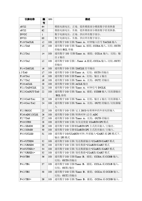
引脚名称编号I/O描述Avcc 64模拟电源电压,正端。
提供模拟部分模拟数字的变换器AVSS 62模拟电源电压,负极。
提供模拟部分模拟数字的变换器。
DVCC 1数字电源电压,正端。
供应所有数字部分。
DVSS 63数字电源电压,负极。
供应所有数字部分。
P1.0/TACLK 12I / O通用数字I / O引脚/ Timer_A,时钟输入信号TACLK输入P1.1/TA0 13 I / O通用数字I / O引脚/Timer_A,捕捉:CCI0A输入,比较:OUT0的输出/ BSL传输P1.2/TA1 14I / O通用数字I / O引脚/ Timer_A,捕捉:CCI1A输入,比较:输出1输出P1.3/TA2 15 I / O通用数字I / O引脚/,Timer_A捕捉:CCI2A输入,比较:OUT2的输出P1.4/SMCLK 16I / O通用数字I / O引脚/ SMCLK信号输出P 1.5/TA0 17 I / O通用数字I / O引脚/ Timer_A,比较:OUT0的输出P1.6/TA1 18I / O通用数字I / O引脚/ Timer_A,比较:输出1输出P1.7/TA2 19I / O通用数字I / O引脚/ Timer_A,比较:OUT2的输出P2.0/ACLK 20I / O通用数字I / O引脚/ ACLK输出P2.1/TAINCLK 21I / O通用数字I / O引脚/ Timer_A,时钟信号INCLKP2.2/CAOUT/TA0 22 I / O通用数字I / O引脚/ Timer_A,捕捉:CCI0B输入/比较器输出/ BSL接收P2.3/CA0/TA1 23 I / O通用数字I / O引脚/ Timer_A,比较:输出1输出/比较器输入P2.4/CA1/TA2 24I / O通用数字I / O引脚/ Timer_A,比较:OUT2的输出/比较器输入P2.5/ROSC 25I / O通用数字I / O引脚/定义DCO标称频率的外部电阻输入P2.6/ADC12CLK 26I / O通用数字I / O引脚/转换时钟- 12位ADC P2.7/TA0 27I / O通用数字I / O引脚/ Timer_A,比较:OUT0的输出P3.0/STE0 28I / O通用数字I / O引脚/从发送使能-USART0/SPI模式P3.1/SIMO0 29I / O通用数字I / O引脚/USART0/SPI方式的从输入/主输出。