motor driver电机驱动原理图
- 格式:pdf
- 大小:63.54 KB
- 文档页数:1

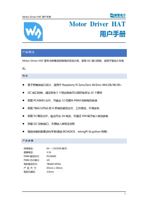
Motor Driver HAT用户手册产品概述Motor Driver HAT是专为树莓派控制电机而设计的,使用I2C接口控制,适用于驱动小车电机。
特点⚫基于树莓派接口设计,适用于Raspberry Pi Zero/Zero W/Zero WH/2B/3B/3B+⚫I2C接口控制,通过改变5个地址跳线可以同时接多达32个模块⚫板载PCA9685芯片,可输出12位硬件PWM控制电机转速⚫板载TB6612FNG双H桥电机驱动芯片,工作高效,不易发热⚫板载5V稳压芯片,输出可达3A电流,可通过VIN端子接入电池供电⚫预留I2C控制接口,方便接入其他主控板⚫提供完善的配套资料手册(提供BCM2835、wiringPi与python例程)产品参数供电电压:6V ~ 12V(VIN端子)逻辑电压: 3.3VPWM驱动芯片:PCA9685PWM芯片接口:I2C电机驱动芯片:TBA6612FNG产品尺寸:65mm x 30mm固定孔通径: 3.0mm接口说明模块实物图如下:硬件资源硬件上实际上由三部分构成:电源、PWM、电机驱动电源输入端采用MP1584稳压芯片,该芯片支持4.5V到28V的宽电压输入,输出电流达3A。
虽然芯片支持最高28V的输入,但是由于给电机的工作电压也由VIN_USER供给,实际上输入电压最好保持在6-12V.MP1584稳压芯片输出5V,这个5V用于给树莓派供电,然后5V再通过RT9193-33转成3.3V电平,该电平给PWM、电机驱动这两部分提供逻辑电压PWM由于树莓派硬件PWM只有一个引脚GPIO.1,而且,虽然wiringPi库与python都有软件PWM,但是会占用部分CPU资源,因此本模块采用PCA9685芯片,该芯片使用I2C控制,可输出16路12位分辨率的PWM,可控制输出频率40HZ-1000HZ。
操作简单,只需要给芯片控制对应寄存器的值,即可一直输出PWM信号。
根据上面的原理图,我们可以看出LED0-LED5为控制电机驱动芯片管脚。
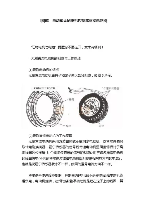
「图解」电动车无刷电机控制器驱动电路图“旺材电机与电控”提醒您不要走开,文末有福利!·无刷直流电动机的组成与工作原理(1)无刷电动机的组成无刷直流电动机由转子和定子两大部分组成,如图3所示。
(2)无刷直流电动机的工作原理无刷直流电动机采用方波自控式永磁同步电动机,以霍尔传感器取代电刷换向器,霍尔传感器的信号线传递电动机里面磁钢相对于绕组线圈的位根据3个霍尔传感器的信号能知道此时应该怎样给电动机的线圈供电(不同的霍尔信应该给电动机绕组提供相对应方向的电流),也就是说霍尔传感器状态不一样,线圈的置号电流方向不一样。
霍尔信号传递给控制器,控制器通过粗线(不是霍尔线)给电动机绕组供电,电动机旋转,磁钢与绕组(准确地说是缠在定子上的线圈,其实霍尔一般安装在定子上)发生转动,霍尔传感器感应出新的位置信号,控制器粗线又给重新改变电流方向的电动机绕组供电,电动机继续旋转(当绕组和磁钢的位置发生变化时,绕组必须对应地改变电流方向,这样电动机才能继续向一个方向运动,否则电动机就会在某一个位置左右摆动,而不是连续旋转),这个过程就是电子换向。
无刷直流电动机由直流电源供电,借助位置传感器来检测转子的位置,所检测出的信号触发相应的电子换相线路,以实现无接触式换相。
无刷直流电动机用电子开关和位置传感器代替电刷及换向器,将直流电转换成模拟三相交流电,通过调制脉宽,改变其电流大小来改变转速。
直流无刷电机的控制结构直流无刷电机是同步电机的一种,也就是说电机转子的转速受电机定子旋转磁场的速度及转子极数(P)影响:N=120.F/P。
在转子极数固定情况下,改变定子旋转磁场的频率就可以改变转子的转速。
直流无刷电机即是将同步电机加上电子式控制(驱动器),控制定子旋转磁场的频率并将电机转子的转速回授至控制中心反复校正,以期达到接近直流电机特性的方式。
也就是说直流无刷电机能够在额定负载范围内当负载变化时仍可以控制电机转子维持一定的转速。

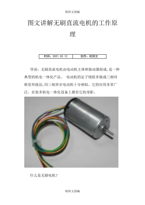
图文讲解无刷直流电机的工作原理时间:2021.03.12 创作:欧阳文导读:无刷直流电机由电动机主体和驱动器组成,是一种典型的机电一体化产品。
电动机的定子绕组多做成三相对称星形接法,同三相异步电动机十分相似。
它的应用非常广泛,在很多机电一体化设备上都有它的身影。
什么是无刷电机?无刷直流电机由电动机主体和驱动器组成,是一种典型的机电一体化产品。
由于无刷直流电动机是以自控式运行的,所以不会像变频调速下重载启动的同步电机那样在转子上另加启动绕组,也不会在负载突变时产生振荡和失步。
中小容量的无刷直流电动机的永磁体,现在多采用高磁能级的稀土钕铁硼(NdFeB)材料。
因此,稀土永磁无刷电动机的体积比同容量三相异步电动机缩小了一个机座号。
无刷直流电动机是采用半导体开关器件来实现电子换向的,即用电子开关器件代替传统的接触式换向器和电刷。
它具有可靠性高、无换向火花、机械噪声低等优点,广泛应用于高档录音座、录像机、电子仪器及自动化办公设备中。
无刷直流电动机由永磁体转子、多极绕组定子、位置传感器等组成。
位置传感按转子位置的变化,沿着一定次序对定子绕组的电流进行换流(即检测转子磁极相对定子绕组的位置,并在确定的位置处产生位置传感信号,经信号转换电路处理后去控制功率开关电路,按一定的逻辑关系进行绕组电流切换)。
定子绕组的工作电压由位置传感器输出控制的电子开关电路提供。
位置传感器有磁敏式、光电式和电磁式三种类型。
采用磁敏式位置传感器的无刷直流电动机,其磁敏传感器件(例如霍尔元件、磁敏二极管、磁敏诂极管、磁敏电阻器或专用集成电路等)装在定子组件上,用来检测永磁体、转子旋转时产生的磁场变化。
采用光电式位置传感器的无刷直流电动机,在定子组件上按一定位置配置了光电传感器件,转子上装有遮光板,光源为发光二极管或小灯泡。
转子旋转时,由于遮光板的作用,定子上的光敏元器件将会按一定频率间歇间生脉冲信号。
采用电磁式位置传感器的无刷直流电动机,是在定子组件上安装有电磁传感器部件(例如耦合变压器、接近开关、LC谐振电路等),当永磁体转子位置发生变化时,电磁效应将使电磁传感器产生高频调制信号(其幅值随转子位置而变化)。


LV8729VOverviewThe LV8729V is a PWM current-controlled microstep bipolar stepping motor driver.This driver can perform eight times of excitation of the second phase to 32W1-second phase and can drive simply by the CLK input.Features• Single-channel PWM current control stepping motor driver. • BiCDMOS process IC.• Output on-resistance (upper side : 0.35Ω ; lower side : 0.3Ω ; total of upper and lower : 0.65Ω ; Ta = 25°C, I O = 1.8A) • 2-phase, 1-2 phase, W1-2 phase, 2W1-2 phase, 4W1-2 phase, 8W1-2 phase, 16W1-2 phase, 32W1-2 phase excitation are selectable.• Advance the excitation step with the only step signal input. • Available forward reverse control. • Over current protection circuit. • Thermal shutdown circuit. • Input pull down resistance • With reset pin and enable pin.SpecificationsAbsolute Maximum Ratings at Ta = 25°CParameter SymbolConditionsRatings UnitMaximum supply voltage VM max 36V Maximum output peak current I O max 1.8 A Maximum logic input voltage V IN max 6V Maximum VREF input voltage VREF max 6V Maximum MO input voltageV MO max6VContinued on next page.Bi-CMOS LSIPWM Constant-Current Control Stepping Motor DriverContinued from preceding page.Parameter SymbolConditionsRatings UnitMaximum DOWN input voltage V DOWN max 6V Allowable power dissipation Pd max * 3.85W Operating temperature Topr -30 to +85°C Storage temperatureTstg-55 to +150°C* Specified circuit board : 90.0mm ×90.0mm ×1.6mm, glass epoxy 2-layer board, with backside mounting.Allowable Operating Ratings at Ta = 25°CParameter SymbolConditionsRatings UnitSupply voltage range VM 9 to 32V Logic input voltage V IN 0 to 5V VREF input voltage rangeVREF0 to 3VElectrical Characteristics at Ta = 25°C, VM = 24V, VREF = 1.5V RatingsParameter SymbolConditionsmin typ maxUnitStandby mode current drain I M st ST = “L”70 100μA Current drainIM ST = “H”, OE = “H”, no load 3.3 4.6mA Thermal shutdown temperature TSDDesign guarantee150180200°C Thermal hysteresis width ΔTSD Design guarantee 40 °CI IN L V IN = 0.8V 38 15μA Logic pin input currentI IN H V IN = 5V 305070μALogic high-level input voltage V IN H 2.0V Logic low-level input voltage V IN L 0.8V Chopping frequencyFch Cosc1 = 100pF 70100 130kHz OSC1 pin charge/discharge current Iosc171013μAVtup1 0.8 1 1.2V Chopping oscillation circuit threshold voltage Vtdown1 0.30.5 0.7V VREF pin input voltage Iref VREF = 1.5V -0.5 μADOWN output residual voltagr V O 1DOWN Idown = 1mA 40 100mV MO pin residual voltage V O 1MOImo = 1mA40100mV Hold current switching frequency Fdown Cosc2 =1500pF 1.12 1.6 2.08Hz Vtup2 0.8 1 1.2V Hold current switching frequency threshold voltage Vtdown2 0.30.5 0.7V VREG1 output voltage Vreg14.755.3VVREG2 output voltage Vreg2V M 1819 20V Ronu I O = 1.8A, high-side ON resistance 0.35 0.455Ω Output on-resistanceRond I O = 1.8A, low-side ON resistance 0.3 0.39Ω Output leakage current I O leak V M = 36V 50μA Diode forward voltageVD I D = -1.8A11.4V Current setting reference voltageVRFVREF = 1.5V, Current ratio 100%0.2850.30.315VPackage Dimensions unit : mm (typ)3333Pin Assignment1 2 3 4 5 6 7 8 9 10 11 12 13 14 15 16 17 18 19 20 21 2244434241403938373635343332313029282726252423OUT1AVMOUT1A NCPGND1 VREG2NC NCNC VREG1VM1 STVM1 MD1RF1 MD2RF1 MD3OUT1B OEOUT1B RSTOUT2A NCOUT2A FRRF2 STPRF2 OSC1VM2 OSC2VM2 NCNC EMONC DOWNPGND2 MOOUT2B VREFOUT2B SGNDTop viewLV8729VSubstrate Specifications (Substrate recommended for operation of LV8729V)Size : 90mm × 90mm × 1.6mm (two-layer substrate [2S0P]) Material : Glass epoxyCopper wiring density : L1 = 85% / L2 = 90% L1 : Copper wiring pattern diagram L2 : Copper wiring pattern diagramCautions1) The data for the case with the Exposed Die-Pad substrate mounted shows the values when 90% or more of the Exposed Die-Pad is wet.2) For the set design, employ the derating design with sufficient margin.Stresses to be derated include the voltage, current, junction temperature, power loss, and mechanical stresses such as vibration, impact, and tension.Accordingly, the design must ensure these stresses to be as low or small as possible. The guideline for ordinary derating is shown below : (1)Maximum value 80% or less for the voltage rating (2)Maximum value 80% or less for the current rating (3)Maximum value 80% or less for the temperature rating3) After the set design, be sure to verify the design with the actual product.Confirm the solder joint state and verify also the reliability of solder joint for the Exposed Die-Pad, etc.Any void or deterioration, if observed in the solder joint of these parts, causes deteriorated thermal conduction, possibly resulting in thermal destruction of IC.A l l o w a b l e p o w e r d i s s i p a t i o n , P d m a x - WAmbient temperature, Ta - CLV8729VBlock DiagramOO W N M OContinued on next page.Reference describing operation(1) Stand-by functionWhen ST pin is at low levels, the IC enters stand-by mode, all logic is reset and output is turned OFF. When ST pin is at high levels, the stand-by mode is released.(2) STEP pin function(3) Excitation setting methodSet the excitation setting as shown in the following table by setting MD1 pin, MD2 pin and MD3 pin.Input Initial position MD3 MD2 MD1 Mode(Excitation) 1ch current 2ch currentLow Low Low2 phase100% -100%Low Low High 1-2 phase100%0% Low High Low W1-2 phase 100% 0% Low High High 2W1-2 phase 100% 0% High Low Low 4W1-2 phase 100% 0% High Low High 8W1-2 phase 100% 0% High High Low 16W1-2 phase 100% 0% High High High 32W1-2 phase 100%0%The initial position is also the default state at start-up and excitation position at counter-reset in each excitation mode. (4) Output current settingOutput current is set shown below by the VREF pin (applied voltage) and a resistance value between RF1(2) pin and GND.I OUT = ( VREF / 5 ) / RF1 (2) resistance* The setting value above is a 100% output current in each excitation mode. (Example) When VREF = 1.1V and RF1 (2) resistance is 0.22Ω, the setting is shown below.I OUT = ( 1.1V / 5 ) / 0.22Ω = 1.0A(5) Output enable functionWhen the OE pin is set Low, the output is forced OFF and goes to high impedance. However, the internal logic circuits are operating, so the excitation position proceeds when the STP is input. Therefore, when OE pin is returned to High, the output level conforms to the excitation position proceeded by the STP input.OE Power save mode0%STEPMONI1ch output2ch outputOutput is high-impedance(6) Reset functionWhen the RST pin is set Low, the output goes to initial mode and excitation position is fixed in the initial position for STP pin and FR pin input. MO pin outputs at low levels at the initial position. (Open drain connection)(7) Forward / reverse switching functionFR Operating mode Low Clockwise (CW) High Counter-clockwise (CCW)The internal D/A converter proceeds by a bit on the rising edge of the step signal input to the STP pin. In addition, CW and CCW mode are switched by FR pin setting.In CW mode, the channel 2 current phase is delayed by 90° relative to the channel 1 current. In CCW mode, the channel 2 current phase is advanced by 90° relative to the channel 1 current.(8) EMO, DOWN, MO output pinThe output pin is open -drain connection. When it becomes prescribed, it turns on, and each pin outputs the Low level.Pin state EMODOWN MO LowAt detection of over-currentHolding current stateInitial positionOFF Normal stateNormal state Non initialpositionRST RESET 0%STEPMONI1ch output2ch output FR STEPExcitation position 1ch output2ch output(1)(2)(3)(4)(5)(6)(5)(4)(3)(4)(5)(9) Chopping frequency setting functionChopping frequency is set as shown below by a capacitor between OSC1 pin and GND.Fcp = 1 / ( Cosc1 / 10 х 10-6 ) (Hz) (Example) When Cosc1 = 200pF, the chopping frequency is shown below.Fcp = 1 / ( 200 х 10-12 / 10 х 10-6 ) = 50(kHz) (10) Output current vector locus (one step is normalized to 90 degrees)Current setting ratio in each excitation mode32W1-2 phase(%) 16W1-2 phase(%) 8W1-2 phase(%)4W1-2phase(%)2W1-2phase (%)W1-2phase (%) 1-2 phase (%) 2phase (%)STEP1ch 2ch 1ch 2ch 1ch 2ch1ch 2ch 1ch 2ch 1ch 2ch 1ch 2ch 1ch 2ch θ0 100 0 100 0 100 0100010001000 100 0θ1 100 1 θ2 100 2 100 2θ3 100 4 θ4 100 5 100 5 100 5 θ5 100 6 θ6 100 7 100 7 θ7 100 9 θ8 100 10 100 10 100 1010010θ9 99 11 θ10 99 12 99 12 θ11 99 13 θ12 99 15 99 15 99 15 θ13 99 16 θ14 99 17 99 17 θ15 98 18 θ16 98 20 98 20 98 2098209820θ17 98 21 θ18 98 22 98 22 θ19 97 23 θ20 97 24 97 24 97 24 θ21 97 25 θ22 96 27 96 27 θ23 96 28 θ24 96 29 96 29 96 299629θ25 95 30Continued on next page.C h a n n e l 1 c u r r e n t r a t i o (%)Channel 2 current ratio (%)θ26 95 31 95 31θ27 95 33θ28 94 34 94 34 94 34θ29 94 35θ30 93 36 93 36θ31 93 37θ32 92 38 92 38 92 38 923892389238θ33 92 39θ34 91 41 91 41θ35 91 42θ36 90 43 90 43 90 43θ37 90 44θ38 89 45 89 45θ39 89 46θ40 88 47 88 47 88 47 8847θ41 88 48θ42 87 49 87 49θ43 86 50θ44 86 51 86 51 86 51θ45 85 52θ46 84 53 84 53θ47 84 55θ48 83 56 83 56 83 56 83568356θ49 82 57θ50 82 58 82 58θ51 81 59θ52 80 60 80 60 80 60θ53 80 61θ54 79 62 79 62θ55 78 62θ56 77 63 77 63 77 63 7763θ57 77 64θ58 76 65 76 65θ59 75 66θ60 74 67 74 67 74 67θ61 73 68θ62 72 69 72 69θ63 72 70θ64 71 71 71 71 71 71 71717171717171 71 100100θ65 70 72θ66 69 72 69 72θ67 68 73θ68 67 74 67 74 67 74θ69 66 75θ70 65 76 65 76θ71 64 77θ72 63 77 63 77 63 77 6377θ73 62 78θ74 62 79 62 79θ75 61 80θ76 60 80 60 80 60 80θ77 59 81θ78 58 82 58 82θ79 57 82θ80 56 83 56 83 56 83 56835683θ81 55 84θ82 53 84 53 84θ83 52 85θ84 51 86 51 86 51 86θ85 50 86θ86 49 87 49 87θ87 48 88θ88 47 88 47 88 47 88 4788θ89 46 89θ90 45 89 45 89Continued on next page.θ91 44 90θ92 43 90 43 90 43 90θ93 42 91θ94 41 91 41 91θ95 39 92θ96 38 92 38 92 38 92 389238923892θ97 37 93θ98 36 93 36 93θ99 35 94θ100 34 94 34 94 34 94θ101 33 95θ102 31 95 31 95θ103 30 95θ104 29 96 29 96 29 96 2996θ105 28 96θ106 27 96 27 96θ107 25 97θ108 24 97 24 97 24 97θ109 23 97θ110 22 98 22 98θ111 21 98θ112 20 98 20 98 20 98 20982098θ113 18 98θ114 17 99 17 99θ115 16 99θ116 15 99 15 99 15 99θ117 13 99θ118 12 99 12 99θ119 11 99θ120 10 100 10 100 10 10010100θ121 9 100θ122 7 100 7 100θ123 6 100θ124 5 100 5 100 5 100θ125 4 100θ126 2 100 2 100θ127 1 100θ128 0 100 0 100 0 1000100010001000 100(11) Current wave example in each excitation mode ( 2 phase, 1-2 phase, 4W1-2 phase, 32W1-2 phase)2-phase excitation (CW mode)1-2 phase excitation (CW mode)STPMO l1(%)(%)-100-1001001000I2STP MO I1(%)-100-100100(%)10000I24W1-2 phase excitation ( CW mode ) 32W1-2 phase excitation ( CW mode )STPMOI1-100(%)10050-500I2-100(%)10050-500STP MOI1-100(%)10050-500I2-100(%)10050-50(12) Current control operation ( Sine-wave increasing direction )Each of current modes operates with the follow sequence.· The IC enters CHARGE mode at a rising edge of the chopping oscillation. ( A period of CHARGE mode (Blanking Time) is forcibly present in approximately 1μs, regardless of the current value of the coil current (ICOIL) and set current (IREF)).· In a period of Blanking Time, the coil current (ICOIL) and the setting current (IREF) are compared.If an ICOIL < IREF state exists during the charge period:The IC operates in CHARGE mode until ICOIL ≥ IREF. After that, it switches to SLOW DECAY mode and then switches to FAST DECAY mode in the last approximately 1μs of the period. If no ICOIL < IREF state exists during the charge period:The IC switches to FAST DECAY mode and the coil current is attenuated with the FAST DECAY operation until the end of a chopping period.The above operation is repeated. Normally, in the sine wave increasing direction the IC operates in SLOW (+ FAST) DECAY mode, and in the sine wave decresing direction the IC operates in FAST DECAY mode until the current is attenuated and reaches the set value and the IC operates in SLOW (+ FAST) DECAY mode.fchop STP fchop STP(13) Output short-circuit protection circuitBuilt-in output short-circuit protection circuit makes output to enter in stand-by mode. This function prevents the IC from damaging when the output shorts circuit by a voltage short or a ground short, etc. When output short state is detected, short-circuit detection circuit state the operating and output is once turned OFF. Subsequently, the output is turned ON again after the timer latch period ( typ. 256μs ). If the output remains in the short-circuit state, turn OFF the output, fix the output to the wait mode, and turn ON the EMO output.When output is fixed in stand-by mode by output short protection circuit, output is released the latch by setting ST = “L”.(14) Open-drain pin for switching holding currentThe output pin is an open-drain connection.This pin is turned ON when no rising edge of STP between the input signals while a period determined by a capacitor between OSC2 and GND, and outputs at low levels.The open-drain output in once turned ON, is turned OFF at the next rising edge of STP.Holding current switching time ( Tdown ) is set as shown below by a capacitor between OSC2 pin and GND.Tdown = Cosc2 х 0.4 х 109 (s)(Example) When Cosc2 = 1500pF, the holding current switching time is shown below.Tdown = 1500pF х 0.4 х 109 = 0.6 (s)Application Circuit ExampleThe above sample application circuit is set to the following conditions: · Output enable function fixed to the output state ( OE = “H” )· Reset function fixed to the output state ( RST = “H” )· Chopping frequency : 50kHz ( Cosc1 = 200pF )The set current value is as follows :I OUT = ( Current setting reference voltage / 5 ) / 0.22ΩMeasurement circuit diagram Stand-by mode current drain : I M stn Current drain : I MTurn OFF SW when measuring I M stn. Turn ON SW when measuring I MLogic pin input current : I IN L, I IN HSet V IN = 0.8V when measuring I IN L.Set V IN = 5V when measuring I IN HThis measurement is related to the ST pin. Take the same procedure for measurement of other pins.Logic input high-level voltage : V IN H ( ST, OE ) Logic input low-level voltage : V IN L ( ST, OE )To measure the ST pin, set SW1 to the ”a” side and SW2 to the ”b” side. To measure the OE pin, set SW1 to the ”b” side and SW2 to the ”a” side.V IN H : When V IN is raised gradually from 0V, the V OUT 1A voltage changes from ”L” to ”H”. The V IN voltage atwhich the voltage changes from ”L” to ”H” is the V IN H voltage.V IN L : When V IN is raised gradually from 3V, the V OUT 1A voltage changes from ”H” to ”L”. The V IN voltage atwhich the voltage changes from ”H” to ”L” is the V IN L voltage.5VV INLogic input high-level voltage : V IN H ( MD1, MD2, MD3 ) Logic input high-level voltage : V IN L ( MD1, MD2, MD3 )V IN H : When V IN is raised gradually from 0V, the V OUT 2B voltage changes from ”H” to ”L”. The V IN voltage atwhich the voltage changes from ”H” to ”L” is the V IN H voltage.V IN L : When V IN is raised gradually from 3V, the V OUT 2B voltage changes from ”L” to ”H”. The V IN voltage atwhich the voltage changes from ”L” to ”H” is the V IN L voltage. This measurement is related to the MD1 pin. Take the same procedure for measurement of MD2 and MD3 pins.24VREG1 output voltage : Vreg1 REG2 output voltage : Vreg2 VREF pin input voltage : IrefCopping frequency : FchMO pin residual voltage : V O lMOOutput on-resistance : Ronu,RondWhen measuring OUT1A upper and OUT2B upper FETs, set SW1 to 4 to the ”a” side. When measuring OUT1A lower and OUT2B lower FETs, set SW1 to 4 to the ”b” side.This measurment is related to OUT1A and OUT2B. To measure OUT2A and OUT1B, enter two rectangular waves to the STP pin and carry out the procedure for measurement.24V 5VCurrent setting reference voltage : VRFRaise the RF1 (2) pin voltage from 0V. The RF1 (2) voltage at which tje OUT voltage changes from ”H” to ”L” is VRF.24V 5VThis catalog provides information as of February, 2011. Specifications and information herein are subject to change without notice.。
MOTOR DRIVERKND- BD3M三相混合伺服式步进电机驱动器用 户 手 册 北京凯恩帝数控技术有限责任公司G07B-W00N-0001KND LTD,2006网址(Http) : E-mail :bj@C注意 !阅读 请详细阅读本说明书后,再进行安装连接。
!!!安全事项 ★驱动器未接电机时,严禁通电! ★严禁带电对驱动器进行任何拨码设置或进行测量! ★必须在断电三分钟后,接线,安装和拨码设置! ★二次开关机之间须有三分钟间隔,以免发生故障报警! ★驱动器的输入电压需满足技术要求! ★通电前,确保电源电缆,电机动力电缆,信号电缆连接正确,且连接紧固! ★通电前,电缆联接完毕后,用万用表电阻档测量驱动器U,V,W端子与FG之间电阻应为无穷大。
用万用表最小电阻档测量驱动器U,V,W端子每两相电阻值应相等。
避免电机相间短路,或电机缺相引起驱动器损坏! ☆本手册内容适用于驱动器软件V3.0版本。
目录 一、性能简介…………………………………………………………………………第1页 二、电气技术参数……………………………………………………………………第1页 三、外观尺寸…………………………………………………………………………第2页 四、接口信号说明……………………………………………………………………第3页 五、拨码开关设置……………………………………………………………………第5页 六、功率接口…………………………………………………………………………第6页 七、状态指示灯………………………………………………………………………第6页 八、驱动器使用注意事项……………………………………………………………第7页 九、BD3M与KND1,10,100系列数控系统的连接……………………………第8页 十、BD3M配KND1,10,100系列数控系统的开关设定………………………第8页 一、性能简介 混合式步进电机采用稀土永磁材料制造,与反应式步进电机相比具有电磁损耗小、转换频率高、动态特性好等优点。
L6203直流电机控制驱动器【简要说明】一、尺寸:长66mmX宽33mm X高28mm二、主要芯片:L6203三、工作电压:控制信号直流4.5~5.5V;驱动电机电压7.2~30V四、可驱动直流(7.2~30V之间电压的电机)五、最大输出电流4A六、最大输出功率20W七、特点:1、具有信号指示2、转速可调3、抗干扰能力强4、具有续流保护5、可单独控制一台直流电机6、PWM脉宽平滑调速(可使用PWM信号对直流电机调速)7、可实现正反转8、此驱动器非常时候控制飞思卡尔智能车,驱动器压降小,电流大,驱动能力强。
【标注图片】直流电机的控制实例使用驱动器可以控制一台直流电机。
电机分别为OUT1和OUT2。
输入端EN可用于输入PWM脉宽调制信号对电机进行调速控制。
(如果无须调速可将EN使能端,接高低电平,高电平启动,低电平停止。
也可由单片机输出直接控制)实现电机正反转就更容易了,输入信号端IN1接高电平输入端IN2接低电平,电机正转。
(如果信号端IN1接低电平,IN2接高电平,电机反转。
)可参考下图表:直流电机测试程序【原理图】【测试程序】汇诚科技实现功能:调试程序使用芯片:AT89S52 或者 STC89C52晶振:11.0592MHZ编译环境:Keil作者:zhangxinchun淘宝店:汇诚科技#include<reg52.h>#define uchar unsigned char//宏定义无符号字符型#define uint unsigned int //宏定义无符号整型sbit P2_0=P2^0;//启动sbit P2_1=P2^1;//停止sbit P2_2=P2^2;//正转sbit P2_3=P2^3;//反转sbit P1_0=P1^0;//使能sbit P1_1=P1^1;//IN1sbit P1_2=P1^2;//IN2延时函数void delay(uchar t)//延时程序uchar m,n,s;for(m=t;m>0;m--)for(n=20;n>0;n--)for(s=248;s>0;s--);主函数main()while(1)if(P2_0==0){delay(3);if(P2_0==0)//启动 P1_0=1;P1_1=1;P1_2=0;if(P2_1==0){delay(3);if(P2_1==0)//停止P1_0=0;if(P2_2==0){delay(3);if(P2_2==0)//正转 P1_1=1;P1_2=0;if(P2_3==0){delay(3);if(P2_3==0)//反转P1_1=0;P1_2=0;结束L6203DMOS(消耗型金属氧化物半导体)全控桥驱动器⏹供电电压:48V⏹最大峰值电流5A(L6021最大2A)⏹电流有效值:⏹L6201: 1A; L6202: 1.5A; L6203/L6201PS: 4A ⏹R DS (ON) 电阻值0.3 Ω (室温25 ︒C)⏹击穿电压保护⏹兼容TTL电路⏹运行最高频率100KHz⏹热滞⏹集成逻辑电路使用⏹高效概述L6201是一种应用多源BCD(Bipolar,CMOS,DMOS)技术来控制电机的全控桥驱动器芯片,这种芯片能将独立的DMOS场效应晶体管和CMOS以及二极管集成在一块芯片上。