三星电容料号说明
- 格式:pdf
- 大小:1.01 MB
- 文档页数:35
三星内存颗粒目前使用三星的内存颗粒来生产内存条的厂家非常多,在市场上有很高的占有率。
由于其产品线庞大,所以三星内存颗粒的命名规则非常复杂。
三星内存颗粒的型号采用一个16位数字编码命名的。
这其中用户更关心的是内存容量和工作速率的识别,所以我们重点介绍这两部分的含义。
编码规则:K 4 X X X X X X X X - X X X X X主要含义:第1位——芯片功能K,代表是内存芯片。
第2位——芯片类型4,代表DRAM。
第3位——芯片的更进一步的类型说明,S代表SDRAM、H代表DDR、G代表SGRAM。
第4、5位——容量和刷新速率,容量相同的内存采用不同的刷新速率,也会使用不同的编号。
64、62、63、65、66、67、6A代表64Mbit的容量;28、27、2A代表128Mbit的容量;56、55、57、5A代表256Mbit的容量;51代表512Mbit的容量。
第6、7位——数据线引脚个数,08代表8位数据;16代表16位数据;32代表32位数据;64代表64位数据。
第11位——连线“-”。
第14、15位——芯片的速率,如60为6ns;70为7ns;7B为7.5ns (CL=3);7C为7.5ns (CL=2) ;80为8ns;10 为10ns (66MHz)。
知道了内存颗粒编码主要数位的含义,拿到一个内存条后就非常容易计算出它的容量。
例如一条三星DDR内存,使用18片SAMSUNG K4H280838B-TCB0颗粒封装。
颗粒编号第4、5位“28”代表该颗粒是128Mbits,第6、7位“08”代表该颗粒是8位数据带宽,这样我们可以计算出该内存条的容量是128Mbits(兆数位)× 16片/8bits=256MB(兆字节)。
注:“bit”为“数位”,“B”即字节“byte”,一个字节为8位则计算时除以8。
关于内存容量的计算,文中所举的例子中有两种情况:一种是非ECC内存,每8片8位数据宽度的颗粒就可以组成一条内存;另一种ECC内存,在每64位数据之后,还增加了8位的ECC校验码。
三星电容编码识别你看盘子的料号如下对比:CL 03 B 104 K Q 8 N N N C1 2 3 4 5 6 7 8 9 10 111 系列编码:CL=积层陶瓷电容2 尺寸编码03=0201(0603) 21=0805(2012) 42=1808(4520)05=0402(1005) 31=1206(3216) 43=1812(4532)10=0603(1608) 32=1210(3225) 55=2220(5750)14=0504(1410) 01=0306(0816) 12=0508(1220)3 介质I类 II类C=C0G S=S2H L=S2LP=P2H T=T2HR=R2H U=U2JA=X5R F=Y5VB=X7R X=X6S4 容量电容容量用三位数表示,前面两位为有效数字,第三位为有效数字后"O"的位数如:104 = 1 00000 (单位pF)如果中间一位为R 则表示"."如:4R7 = 4.7pF5 电容的误差:B=±0.1pf F=±1pf±1% K=±10%C=±0.25pf G=±2% M=±20%D=±0.5pf? J=±5% Z=+80/-20%6 额定电压R=4V O =16V B =50V E = 250V I = 1000VQ=6.3V A =25V C=100V G = 500V J = 2000VP =10V L =35V D =200V H = 630V K= 3000V7 厚度:3=0.30毫米 A=0.65毫米 M=1.15毫米 I=2.00毫米 Q=1.25毫米5=0.50毫米 C=0.85毫米 F=1.25毫米 J=2.50毫米 V=2.50毫米8=0.80毫米 D=1.00毫米 H=1.60毫米 L=3.20毫米8 内电极A=常规产品钯/银/镍屏蔽/锡 100%N=常规产品镍/铜/镍屏蔽/锡 100%G=常规产品铜/铜/镍屏蔽/锡 100%L=低侧面产品镍/铜/镍屏蔽/锡 100%9 产品编码A =阵列(2-元素) L =LICCB =阵列(4-元素) N =常规P =自动 C=高频10 特殊编码11 包装编码B=散装 O=纸版箱料带,10英寸料盘 E=压花纸版箱,7英寸料盘P=散装箱 D=纸版箱料带,13英寸料盘(10000ea) F=压花纸版箱,13英寸料盘C=纸版箱料带,7英寸料盘 L=纸版箱料带,13英寸料盘(15,000ea) S=压花纸版箱,10英寸料盘如有侵权请联系告知删除,感谢你们的配合!。

三星帖片电容规格对照表三星帖片电容规格对照表规格试例:CL 10 A 105 K Q 8 N N N C1 2 3 4 5 6 7 8 9 10 111:系列编码CL=积层电容2:尺寸编码英寸 (毫米) 英寸 (毫米) 英寸 (毫米)0.3=0201(0603) 21=0805(2012) 42=1808(4520)0.5=0402(1005) 31=1206(3216) 43=1812(4532)10=0603(1608) 32=1210(3225) 55=2220(5750)3:电介质编码I类II类C=COG S=S2H L=S2L A=X5R F=Y5VP=P2H T=T2H B=X7R X=X6SR=R2H U=U2J4:电容编码以PF表示的电容,2个有效位加上零的数量.例如:106=10X106=10000000PF 对于<10PF,字母R表示小数点.例如;1R5=1.5PF 5:公差编码B=±0.1PF F=±1PF, ±1% K=±10%C=±0.25PF G=±2% M=±20%D=±0.5PF J=±5% Z=+80/-20%对于小于等于10PF的数值,F=±1PF对于大于10PF的数值,F=±1%.6:额定电压编码R=4V O=16V B=50V E=250V I=1000VQ=6.3V A=25V C=100V G=500V J=2000VP=10V L=35V D=200V H=630V K=3000V7:厚度编码3=0.30毫米 A=0.65毫米 M=1.15毫米 I=2.00毫米 Q=1.25毫米5=0.50毫米 C=0.85毫米 F=1.25毫米 J=2.50毫米 V=2.50毫米8=0.80毫米 D=1.00毫米 H=1.60毫米 L=3.20毫米8:内电极/端子/电镀编码A=常规产品钯/银/镍屏蔽/锡100%N=常规产品镍/铜/镍屏蔽/锡100%G=常规产品铜/铜/镍屏蔽/锡100%L=常规产品镍/铜/镍屏蔽/锡100%9:产品编码A=阵列(2-元素) L=L1CC B=阵列(4-元素) N=常规C=高频 P=自动10:特殊编码N=预留给未来用途11:包装编码B=散装 O=纸板箱料带,10英寸料盘 E=压花纸板箱,7英寸料盘P=散装箱D=纸板箱料带,13英寸料盘(10000CA) F=压花纸板。
规格说明:CL=积层陶瓷电容03=0201(0603) 21=0805(2012) 42=1808(4520)05=0402(1005) 31=1206(3216) 43=1812(4532)10=0603(1608) 32=1210(3225) 55=2220(5750)14=0504(1410) 01=0306(0816) 12=0508(1220)电容容量用三位数表示,前面两位为有效数字,第三位为有效数字后"O"的位数如:105 = 10 00000 (单位pF)如果中间一位为R 则表示"."如:3R3 = 3.3pFA=常规产品 钯/银/镍屏蔽/锡 100% N=常规产品 镍/铜/镍屏蔽/锡100%G=常规产品 铜/铜/镍屏蔽/锡 100% L=低侧面产品 镍/铜/镍屏蔽/锡 100%A =阵列(2-元素) L =LICCB =阵列(4-元素) N =常规 P =自动 C=高频预留的用途第1页规格事例:I类符号EIA编码工作温度范围(℃)温度系数范围(ppm/℃)C C0G -55~+125 0±30P P2H -55~+125 -150±60R R2H -55~+125 -220±60S S2H -55~+125 -330±60T T2H -55~+125 -470±60U U2J -55~+125 -750±120L S2L -55~+125 -1000~+350II类符号EIA编码工作温度范围(℃)电容变化(?C%)A X5R -55~+85 ±15B X7R -55~+125 ±15X X6S -55~+105 ±22F Y5V -30~+85 -82~+22**系列TC电容步骤***第2页外型尺寸:特征.尺寸的大小从:从0402到2220;.PCB高可靠公差和高速自动芯片更换;.大电容范围;.大温度补偿和电压范围:从COG到Y5V和从6.3V到50V;.高可靠性性能;.高电阻端子金属;.表面贴装组件的带料和料盘尺寸表示图(值见下表)鈀 MLCC(MLCC=A鈀零件编码第12号).I类电容<10pF(I类。
■INTRODUCTIONMLCC(Multilayer Ceramic Capacitor)is SMD(Surface Mounted Device)type capacitor that is used in wide ranges of capacitance.MLCC is paid more attentions than other capacitors due to the better frequency characteristics,higher reliability,higher withstanding voltage and so on.MLCC is made of many layers of ceramic and inner electrodes like sandwich.Pd was used for inner electrodes.But the price of Pd was skyrocketed and Pd was replaced by the BME(Base Metal Electrode),which reduced the total cost of MLCC.This inner electrode is connected to outer termination for surface mounting,which is composed of three layers,Cu or Ag layer,Ni plating layer,and SnPb or Sn plating layer.Most of MLCCs become Pb free by the environmental issue at present.MLCC is divided into two classes.Class I(C0G,etc)is the temperature compensating type.It hasa small TCC(Temperature Coefficient of Capacitance)and a better frequency performance.Therefore,it is used in RF applications such as cellular phone,tuner,and so on.Class II(X7R, X5R,Y5V,etc)is the high dielectric constant type,which is used in general electronic circuit.Especially high capacitance MLCC is replacing other capacitors(Tantalum and Aluminum capacitor)due to the low ESR(Equivalent Series Resistance)value.■FEATURE AND APPLICATION●Feature-Miniature Size-Wide Capacitance and Voltage Range-Highly Reliable Performance-Tape&Reel for Surface Mount Assembly-Low ESR-High Q at High Frequencies-Stable Temperature Dependence of Capacitance●Application-High Frequency Circuit(Tuner,VCO,PAM etc)-General Power Supply Circuit(SMPS etc)-DC-DC Converter-General Electronic Circuit■STRUCTURE■APPEARANCE AND DIMENSIONDIMENSION(mm)CODE EIA CODEL W T(MAX)BW 0302010.6±0.030.3±0.030.3±0.030.15±0.05050402 1.0±0.050.5±0.050.5±0.050.2+0.15/-0.1 100603 1.6±0.10.8±0.10.8±0.10.3±0.2210805 2.0±0.1 1.25±0.1 1.25±0.10.5+0.2/-0.3 311206 3.2±0.2 1.6±0.2 1.6±0.20.5+0.2/-0.3 321210 3.2±0.3 2.5±0.2 2.5±0.20.6±0.3431812 4.5±0.4 3.2±0.3 3.2±0.30.8±0.3552220 5.7±0.4 5.0±0.4 3.2±0.3 1.0±0.3■PREVIOUS PART NUMBERINGSymbol EIA Code TemperatureCoefficient(PPM/℃)※TemperatureCharacteristicsOperationTemperature RangeC C0G(CH)0±30C Δ-55~+125℃P P2H -150±60P ΔR R2H -220±60R ΔS S2H -330±60S ΔT T2H -470±60T ΔU U2J -750±120U ΔLS2L+350~-1000SL▶CLASS Ⅰ(Temperature Compensation)TemperatureCharacteristicsbelow 2.0pF 2.2~3.9pF above 4.0pFabove 10pFC ΔC0G C0G C0G C0G P Δ-P2J P2H P2H R Δ-R2J R2H R2H S Δ-S2J S2HS2H T Δ-T2J T2H T2H U Δ-U2JU2JU2JSymbol EIA Code Capacitance Change(ΔC :%)OperationTemperature RangeA X5R ±15-55~+85℃B X7R ±15-55~+125℃FY5V+22~-82-30~+85℃▶CLASS Ⅱ(High Dielectric Constant)SAMSUNG Multilayer Ceramic Capacitor Type(Size)Capacitance Temperature Characteristics Nominal Capacitance Capacitance Tolerance Rated Voltage Thickness Option Packaging Type CAPACITANCE TEMPERATURE CHARACTERISTICS ※Temperature Characteristics ☞K :±250PPM/℃J :±120PPM/℃H :±60PPM/℃G :±30PPM/℃●●●●●●●●●Temperature CharacteristicsSymbol Tolerance Applicable Capacitance &RangeC0G(NPO)or T.C SeriesB ±0.1pF 0.5~3pF C±0.25pF 0.5~10pF D ±0.5pF F ±1pF 6~10pFG ±2%E-24Series for over 10pF J ±5%K±10%A(X5R)B(X7R)J ±5%E-12SeriesK ±10%M ±20%F(Y5V)Z-20%~+80%E-6Series CAPACITANCE TOLERANCE The nominal capacitance value is expressed in pico-Farad(pF)and identified by three-digit number,first two digits represent significant figures and last digit specifies the number of zeros to follow.For values below 1pF,the letter "R"is used as the decimal point and the last digit becomes significant.example)100:10×10o =10pF 102:10×102=1000pF020:2×10o =2pF1R5:1.5pFNOMINAL CAPACITANCE ●●※Please consult us for special tolerances.RATED VOLTAGE ●PACKAGING TYPE THICKNESS OPTION Symbol Description of the CodeN Standard thickness (please refer to standard thickness table on next page)A Thinner than standard thickness B Thicker than standard thicknessC Standard Thickness High Q (Low `D.F `)D Sn-100%(High-Q)ESn-100%(General)※Please Consult us for other termination type.●●Series Capacitance StepE-3 1.02.24.7E-6 1.01.52.23.34.76.8E-12 1.0 1.2 1.5 1.8 2.2 2.7 3.3 3.9 4.7 5.6 6.88.2E-241.0 1.2 1.5 1.82.2 2.73.3 3.94.75.66.88.21.11.31.62.02.43.03.64.35.16.27.59.1※Standard Capacitance is "Each step ×10n "▶STANDARD CAPACITANCE STEP■NEW PART NUMBERING●PRODUCT ABBREVIATION Symbol Product AbbreviationCLSAMSUNG Multilayer Ceramic Capacitor●SIZE(mm)Symbol Size(mm)Length Width 030.60.305 1.00.510 1.60.821 2.0 1.231 3.2 1.632 3.2 2.543 4.5 3.2555.75.0SAMSUNG Multilayer Ceramic Capacitor Size(mm)Capacitance Temperature Characteristic Nominal Capacitance Capacitance Tolerance Rated Voltage Thickness Option Product &Plating Method Samsung Control Code Reserved For Future Use Packaging Type ●●●●●●●●●●●●CAPACITANCE TEMPERATURE CHARACTERISTICSymbol Temperature Characteristics Temperature RangeCClassⅠCOG C△0±30(ppm/℃)-55~+125℃P P2H P△-150±60R R2H R△-220±60S S2H S△-330±60T T2H T△-470±60U U2J U△-750±60L S2L S△+350~-1000AClassⅡX5R X5R±15%-55~+85℃B X7R X7R±15%-55~+125℃F Y5V Y5V+22~-82%-30~+85℃※Temperature CharacteristicTemperatureCharacteristicsBelow2.0pF 2.2~3.9pF Above4.0pF Above10pF CΔC0G C0G C0G C0GPΔ-P2J P2H P2HRΔ-R2J R2H R2HSΔ-S2J S2H S2HTΔ-T2J T2H T2HUΔ-U2J U2J U2JJ:±120PPM/℃,H:±60PPM/℃,G:±30PPM/℃●NOMINAL CAPACITANCENominal capacitance is identified by3digits.The first and second digits identify the first and second significant figures of the capacitance. The third digit identifies the multiplier.'R'identifies a decimal point.●ExampleSymbol Nominal Capacitance1R5 1.5pF10310,000pF,10nF,0.01μF104100,000pF,100nF,0.1μF●CAPACITANCE TOLERANCE Symbol Tolerance Nominal CapacitanceA ±0.05pF Less than 10pF (Including 10pF)B ±0.1pFC ±0.25pFD ±0.5pF F ±1pF F ±1%More than 10pF G ±2%J ±5%K ±10%M ±20%Z+80,-20%●RATEDVOLTAGE●THICKNESS OPTIONType Symbol Thickness(T)Spec 060330.30±0.03 100550.50±0.05 160880.80±0.102012A0.65±0.10 C0.85F 1.25±0.103216C0.85±0.15 F 1.25±0.15 H 1.6±0.203225F 1.25±0.20H 1.6I 2.0J 2.54532F 1.25±0.20H 1.6I 2.0J 2.5L 3.2±0.305750F 1.25±0.20H 1.6I 2.0J 2.5L 3.2±0.30●PRODUCT&PLATING METHODSymbol Electrode Termination Plating TypeA Pd Ag Sn_100%N Ni Cu Sn_100%G Cu Cu Sn_100%●SAMSUNG CONTROL CODE●RESERVED FOR FUTURE USESymbol Description of the codeN Reserved for future use●PACKAGING TYPE▶CAPACITANCE vs CHIP THICKNESS STANDARDDescription0603(0201)1005(0402)1608(0603)2012Type (0805)3216Type (1206)3225Type (1210)4532Type (1812)5750Type (2220)Dimension (mm)L0.6±0.03 1.0±0.05 1.6±0.1 2.0±0.13.2±0.153.2±0.2 3.2±0.34.5±0.45.7±0.4W 0.3±0.030.5±0.050.8±0.1 1.25±0.1 1.6±0.15 1.6±0.22.5±0.23.2±0.3 5.0±0.4T0.3±0.030.5~±0.050.8±0.10.65±0.10.85±0.11.25±0.10.85±0.15 1.25±0.15 1.6±0.21.25±0.2 1.6±0.22.0±0.22.5±0.21.25±0.21.6±0.22.0±0.22.5±0.21.6±0.22.0±0.22.5±0.2C A P ACIT A N CER A N G E (p F )SL 50V -0.5~2400.5~10000.5~10001100~15001600~27000.5~27003000~56006200~8200-----------C,TC (Except SL,UJ)25V 0.5~470.5~2200.5~1000--3300~82001500~36003900~68007500~10000-----100000-----50V -0.5~1800.5~10000.5~560620~10001100~33000.5~22002400~4700-560~1000011000~2200024000~47000-1000~1300015000~2200024000~4700062000~680004300093000130000C A P A C I T A N C E R A N G E (n F )A (X5R)6.3V 102202200--10000--10000---22000---47000--4700010V101001000--2200--4700~10000---22000------4700016V -47330~470--1000--4700---6800~10000-------25V --------------------50V- 6.8~10------------------B (X7R)6.3V 0.1~1047~100470~1000--1000--6800~10000---22000-------10V0.1~1033~100220~470220~270330~470560~1000-1000~330047001500~220033003900~4700----22000---16V0.1~110~33100~22068~200220~330390~1000330~6801000~15002200~33001500~220033003900~4700---2200----25V -4.7~1047~10039~6882~100150~470100~330470~620680~1000680~150018002200---1000---1000050V -0.22~4.70.22~1000.22~3947~1002201~150220390~1000 2.2~680820~1000--10~1000-----3300~4700F (Y5V)6.3V10~100-2200--10000-----47000--------10V -220~330100~1000--4700-470010000~22000---22000------10000016V -10~220100~100010~680820~10001200~22001000~22002700~4700100003300~68001000015000---22000----25V -10~3322~33010~220270~470560~1000470~10001200~22002700~33001000~33004700~10000-----10000---50V - 2.2~102.2~1002.2~6882~150180~100010~470560~1000-100~1000------10000---■PACKAGING●CARDBOARD PAPER TAPESymbol W F E P1P2P0D tABTypeD i m e n s i o n038.0±0.3 3.5±0.05 1.75±0.12.0±0.052.0±0.05 4.0±0.1Φ1.5+0.1/-00.37±0.030.38±0.030.68±0.03050.6±0.050.65+0.05/-0.1 1.15+0.05/-0.110 4.0±0.11.1MAX1.1±0.21.9±0.221 1.6±0.22.4±0.2312.0±0.23.6±0.2unit :mm●EMBOSSED PLASTIC TAPE●TAPING SIZE●REEL DIMENSIONSymbol A B CDEWtR7"Reel φ178±2.0min.φ50φ13±0.521±0.82.0±0.510±1.50.8±0.21.013"Reelφ330±2.0min.φ70unit :mmSymbol Cardboard Paper TapeEmbossed Plastic Tape7"Reel 4000200013"Reel15000-unit :pcsSize 05(0402)10(0603)21(0805)T ≤0.85mm T ≥1.0mm Quantity 50,00010,000~15,000*10,0005,000●BULK CASE PACKAGING-Bulk case packaging can reduce the stock space and transportation costs.-The bulk feeding system can increase the productivity.-It can eliminate the componentsloss.Symbol A B T C D E Dimension 6.8±0.18.8±0.112±0.1 1.5+0.1/-02+0/-0.14.7±0.1Symbol F W G H L I Dimension31.5+0.2/-036+0/-0.219±0.357±0.35110±0.75±0.35●QUANTITY*Option■CHARACTERISTIC MAP●CLASSⅠTemperature Characteristics Size VoltageCapacitance Range(㎊)SL,UJ05 (0402)50V10 (0603)50V21 (0805)50V31 (1206)50VC(COG)& TC Series03(0201)25V05(0402)25V50V10(0603)25V50V21(0805)25V50V31(1206)25V50V 32(1210)50V100V43(1812)25V50V55(2220)50V101001000100001000001000000100000001000000000.5240270082001000100010000150033004700100018022047820033001800047005604700068000100010000013000043000●CLASSⅡ,A(X5R)Temperature Characteristics Size Voltage Capacitance Range(㎊)A(X5R)0603(0201)6.3V10V1005(0402)6.3V10V16V50V1608(0603)6.3V10V16V2012(0805)6.3V10V16V3216(1206)6.3V10V16V3225(1210)6.3V10V16V4532(1812) 6.3V5750(2220)6.3V10V101001000100001000001000000100000001000000001000010000010000100000004700000220000002200000100000004700000220000004700000047000100006800100000022000001000000470000330000100000001000000068000004700000047000000220000●CLASSⅡ,B(X7R)Temperature Characteristics Size VoltageCapacitance Range(㎊)B(X7R)03(0201)6.3V10V16V05(0402)6.3V10V16V25V50V10(0603)6.3V10V16V25V50V21(0805)6.3V10V16V25V50V31(1206)6.3V10V16V 25V50V10100100010000100000100000010000000100000000100000470004700000470000100000100000047000022000010000003300000100000010000001001000010000000100000100000100100001001000680000033000100003300010000470047002204700002200002200001000004700022022000010000006800039000220100000033000010000010000001000●CLASSⅡ,B(X7R)Temperature Characteristics Size VoltageCapacitance Range(㎊)B(X7R)32(1210)6.3V10V16V25V50V43(1812)10V16V25V50V55(2220)25V50V1010010001000010000010000001000000010000000022000000100000010000470000015000002200000010000001000000047000003300000470000015000002200000680000100000022002200000●CLASSⅡ,F(Y5V)Temperature Characteristics Size VoltageCapacitance Range(㎊)F(Y5V)03(0201) 6.3V05(0402)10V16V25V50V10(0603)6.3V10V16V25V50V21(0805)6.3V10V16V25V50V31(1206)10V16V 25V50V32(1210)6.3V10V16V25V50V43(1812)16V25V50V55(2220)10V330000330001000022000010000220010000003300001000001000002200022001000000220000010000100002200000047000001000000033000001000000100000047000010000470000010000001500000033000001000000100000100000002200000010000220000100000001000000010000000022000001000000010000010000100000010000010000002200470000002200000010100100010000100000100000010000000100000000■RELIABILITY TEST DATANO ITEM PERFORMANCE TEST CONDITION 1APPEARANCE NO ABNORMAL EXTERIOR APPEARANCE THROUGH MICROSCOPE(×10)2INSULATIONRESISTANCE10,000㏁OR500㏁∙㎌PRODUCT WHICHEVER ISSMALLER(RATED VOLTAGE IS BELOW16V:10,000㏁OR100㏁∙㎌)RATED VOLTAGE SHALL BE APPLIED.MEASUREMENT TIME IS60~120RATED VOLTAGETIME60SEC.3WITHSTANDINGVOLTAGENO DIELECTRIC BREAKDOWN ORMECHANICAL BREAKDOWNCLASSⅠ:300%OF THE RATED VOLTAGE FOR1~5SEC,CLASSⅡ:250%OF THE RATED VOLTAGE FOR1~5SECIS APPLIED WITH LESS THAN50㎃CURRENT4CAPACITANCECLASSⅠWITHIN THE SPECIFIEDTOLERANCECAPACITANCE FREQUENCY VOLTAGE1,000㎊ANDBELOW1㎒±10%0.5~5VrmsMORE THAN1,000㎊1㎑±10%CLASSⅡWITHIN THE SPECIFIEDTOLERANCECAPACITANCE FREQUENCY VOLTAGE10㎌AND BELOW1㎑±10% 1.0±0.2VrmsMORE THAN10㎌120㎐±20%0.5±0.1Vrms5Q CLASSⅠOVER30㎊:Q≥1,000LESS THAN30㎊:Q≥400+20C(C:CAPACITANCE)CAPACITANCE FREQUENCY VOLTAGE1,000㎊ANDBELOW1㎒±10%0.5~5VrmsMORE THAN1,000㎊1㎑±10%6TanδCLASSⅡ1.CHAR:B2.CHAR:FCAPACITANCE FREQUENCY VOLTAGE10㎌AND BELOW1㎑±10% 1.0±0.2VrmsMORE THAN10㎌120㎐±20%0.5±0.1Vrms RATED VOLTAGE DF SPEC6.3V0.05max10V0.05max16V0.035max25V0.025max50V이상0.025max6.3V10V16V25V50V1005-0.125max0.09max(C<220nF)0.125max(C≥220nF)0.05max0.05max16080.16max0.125max0.09max0.05max(C≤100nF)0.07max(C>100nF)0.05max20120.16max0.125max0.09max0.07max0.05max32160.16max0.125max0.09max0.07max0.05max32250.16max0.125max0.09max0.07max(C≤6.8㎌)0.09max(C>6.8㎌)0.05max45320.16max0.16max0.09max--57500.125max---*THE INITIAL VALUE OF HIGH DIELECTRIC CONSTANT SERIES SHALL BE MEASUREDAFTER THE HEAT TREATMENT OF150+0/-10℃,1Hr AND SITTING OF48±4hr AT ROOM TEMPERATURE&ROOM HUMIDITY.NO ITEM PERFORMANCE TEST CONDITION14HUMIDITY(STEADYSTATE)APPEARANCE NO MECHANICAL DAMAGE SHALL OCCUR TEMPERATURE:40±2℃RELATIVE HUMIDITY:90~95%RHTEST TIME:500+12/-0Hr.MEASURE AT ROOM TEMPERATUREAFTER COOLING FORCLASSⅠ:24±2Hr.CLASSⅡ:48±4Hr.CAPACITANCECHARACTERISTIC CAPACITANCE CHANGECLASSⅠWITHIN±5%OR±0.5㎊WHICHEVERIS LARGERCLASSⅡA,B WITHIN±12.5%F WITHIN±30%QCLASSⅠ30㎊AND OVER:Q≥35010~30㎊:Q≥275+2.5×CLESS THAN10pF:Q≥200+10×CTanδCLASSⅡINSULATIONRESISTANCEMINIMUM INSULATION RESISTANCE:1,000㏁OR50㏁∙㎌PRODUCT WHICHEVER ISSMALLER15MOISTURERESISTANCEAPPEARANCE NO MECHANICAL DAMAGE SHALL OCCUR APPLIED VOLTAGE:RATED VOLTAGETEMPERATURE:40±2℃RELATIVE HUMIDITY:90~95%RHTEST TIME:500+12/-0Hr.CURRENT APPLIED:50㎃MAX.<INITIAL MEASUREMENT>CLASSⅡSHOULD BE MEASUREDINITIAL VALUE AFTER BE HEAT-TREATEDFOR1HR IN150℃+0/-10℃AND BE LEFTFOR48±4HR AT ROOM TEMPERATURE.<LATTER MEASUREMENT>CLASSⅠSHOULD BE MEASURED AFTERLEFT FOR24±2HRS IN ROOMTEMPERATURE AND HUMIDITY.CLASSⅡSHOULD BE MEASUREDLATTER VALUE AFTER BEHEAT-TREATED FOR1HR IN150℃+0/-10℃AND BE LEFT FOR48±4HR AT ROOMTEMPERATURE.CAPACITANCECHARACTERISTIC CAPACITANCE CHANGECLASSⅠWITHIN±7.5%OR±0.75㎊WHICHEVERIS LARGERCLASSⅡA,B WITHIN±12.5%FWITHIN±30%WITHIN+30~-40%1005C>0.47μF1608C>1.0μF2012C>4.7μF3216C>10.0μF3225C>22.0μF4532C>47.0μFQCLASSⅠ30㎊AND OVER:Q≥20030㎊AND BELOW:Q≥100+10/3×CTanδCLASSⅡINSULATIONRESISTANCEMINIMUM INSULATION RESISTANCE:500㏁OR25㏁∙㎌PRODUCT,WHICHEVER IS SMALLER.CHAR.25VANDOVER16V10V 6.3V4VA,B0.050.05MAX0.05MAX0.075MAX0.1MAXF0.075MAX0.1MAX(C〈1.0㎌)0.125MAX(C≥1.0㎌)0.15MAX0.195MAX0.25MAXCHAR.25VANDOVER16V10V 6.3V4VA,B0.05MAX0.05MAX0.05MAX0.075MAX0.1MAXF0.075MAX0.1MAX(C〈1.0㎌)0.125MAX(C≥1.0㎌)0.15MAX0.195MAX0.25MAX6.3VTanδ0.125MAX*ConditionCLASSⅡ(A,B)1005C≥0.22㎌1608C≥2.2㎌2012C≥4.7㎌3216C≥10.0㎌3225C≥22.0㎌4532C≥47.0㎌5750C≥100.0㎌6.3V Tanδ0.125MAX*ConditionCLASSⅡ(A,B)1005C≥0.22㎌1608C≥2.2㎌2012C≥4.7㎌3216C≥10.0㎌3225C≥22.0㎌4532C≥47.0㎌5750C≥100.0㎌NO ITEM PERFORMANCE TEST CONDITION16HIGHTEMPERATURERESISTANCEAPPEARANCE NO MECHANICAL DAMAGE SHALL OCCURAPPLIED VOLTAGE:150%,200%OF RATED VOLTAGETEST TIME:1000+48/-0Hr.CURRENT APPLIED:50㎃MAX.<INITIAL MEASUREMENT>CLASSⅡSHOULD BE MEASURED INITIALVALUE AFTER BE HEAT-TREATED FOR1HR IN150℃+0/-10℃AND BE LEFT FOR48±4HR AT ROOM TEMPERATURE.<LATTER MEASUREMENT>CLASSⅠSHOULD BE MEASURED AFTERLEFT FOR24±2HRS IN ROOMTEMPERATURE AND HUMIDITY.CLASSⅡSHOULD BE MEASURED LATTERVALUE AFTER BE HEAT-TREATED FOR1HR IN150℃+0/-10℃AND BE LEFT FOR48±4HR AT ROOM TEMPERATURE.(TWICE OF RATED VOLTAGE WILL BEAPPLIED TO ALL SERIES BUT ABOVE)**HOWEVER,A/B는1005C≥0.22㎌SEE(FIG.3)CAPACITANCECHARACTERISTIC CAP.CHANGECLASSⅠWITHIN±3%OR±0.3㎊,WHICHEVER IS LARGERCLASSⅡA,B WITHIN±12.5%FWITHIN±30%WITHIN+30~40%1005C>0.47μF1608C>1.0μF2012C>4.7μF3216C>10.0μF3225C>22.0μF4532C>47.0μFQCLASSⅠ30㎊AND OVER:Q≥35010~30㎊:Q≥275+2.5×CLESS THAN10㎊:Q≥200+10×CTanδCLASSⅡINSULATIONRESISTANCEMINIMUM INSULATION RESISTANCE:1,000㏁OR50㏁∙㎌PRODUCTWHICHEVER IS SMALLER17TEMPERATURECYCLEAPPEARANCE NO MECHANICAL DAMAGE SHALL OCCUR CAPACITORS SHALL BE SUBJECTEDTO FIVE CYCLES OF THETEMPERATURE CYCLE AS FOLLOWINGSTEP TEMP.(℃)TIME(MIN)1MIN.RATEDTEMP.+0/-3302252~33MAX.RATEDTEMP.+3/-0304252~3MEASURE AT ROOM TEMPERATUREAFTER COOLING FORCLASSⅠ:24±2Hr.CLASSⅡ:48±4Hr.CAPACITANCECHARACTERISTIC CAP.CHANGECLASSⅠWITHIN±2.5%OR±0.25㎊WHICHEVER ISLARGERCLASSⅡA,B WITHIN±7.5%F WITHIN±20%QCLASSⅠ30㎊AND OVER:Q≥1000LESS THAN30㎊:Q≥400+20×CTanδCLASSⅡTO SATISFY THE SPECIFIEDINITIAL VALUEINSULATIONRESISTANCETO SATISFY THE SPECIFIEDINITIAL VALUECHAR.25VANDOVER16V10V 6.3V4VA,B0.05MAX0.05MAX0.05MAX0.075MAX0.1MAXF0.075MAX0.1MAX(C<1.0㎌)0.125MAX(C≥1.0㎌)0.15MAX0.195MAX0.25MAXCHAR.TEMP.CLASSⅠ125±3℃CLASSⅡA85±3℃B125±3℃F85±3℃*150%Authorization ConditionsCLASSⅡ(A,B,F)1005C>0.47μF1608C≥2.2㎌2012C≥4.7㎌3216C≥10.0㎌3225C≥22.0㎌4532C≥47.0㎌5750C≥100.0㎌■CHARACTERISTIC GRAPH▶CAPACITANCE CHANGE -AGING▶CAPACITANCE -DC VOLTAGE CHARACTERISTICS▶CAPACITANCE -TEMPERATURE CHARACTERISTICS●ELECTRICAL CHARACTERISTICS■APPLICATION MANUAL●Storage Condition▶Storage EnvironmentThe electrical characteristics of MLCCs were degraded by the environment of high temperature or humidity.Therefore,the MLCCs shall be stored in the ambient temperature and the relative humidity of less than40℃and70%,respectively.Guaranteed storage period is within6months from the outgoing date of delivery.▶Corrosive GasesSince the solderability of the end termination in MLCC was degraded by a chemical atmosphere such as chlorine,acid or sulfide gases,MLCCs must be avoid from these gases.▶Temperature FluctuationsSince dew condensation may occur by the differences in temperature when the MLCCs are taken out of storage,it is important to maintain the temperature-controlled environment.●Design of Land PatternWhen designing printed circuit boards,the shape and size of the lands must allow for theproper amount of solder on the capacitor.The amount of solder at the end terminations has a direct effect on the crack.The crack in MLCC will be easily occurred by the tensile stress which was due to too much amount of solder.In contrast,if too little solder is applied,the termination strength will be e the following illustrations as guidelines for proper land design.Recommendation of Land Shape and Size●AdhesivesWhen flow soldering the MLCCs,apply the adhesive in accordance with the following conditions.▶Requirements for AdhesivesThey must have enough adhesion,so that,the chips will not fall off or move during thehandling of the circuit board.They must maintain their adhesive strength when exposed to soldering temperature.They should not spread or run when applied to the circuit board.They should harden quickly.They should not corrode the circuit board or chip material.They should be a good insulator.They should be non-toxic,and not produce harmful gases,nor be harmful when touched.▶Application MethodIt is important to use the proper amount of adhesive.Too little and much adhesive will cause poor adhesion and overflow into the land,respectively.▶Adhesive hardening CharacteristicsTo prevent oxidation of the terminations,the adhesive must harden at160℃or less,within2minutes or less.●Mounting▶Mounting Head PressureExcessive pressure will cause crack to MLCCs.The pressure of nozzle will be300g maximum during mounting.▶Bending StressWhen double-sided circuit boards are used,MLCCs first are mounted and soldered onto one side of the board.When the MLCCs are mounted onto the other side,it is important to support the board as shown in the illustration.If the circuit board is not supported,the crack occur to the ready-installed MLCCs by the bending stress.●FluxAlthough the solderability increased by the highly-activated flux,increase of activity in flux may also degrade the insulation of the chip capacitors.To avoid such degradation,it is recommended that a mildly activated rosin flux(less than0.2%chlorine)be used.●SolderingSince a multilayer ceramic chip capacitor comes into direct contact with melted solder during soldering,it is exposed to potentially mechanical stress caused by the sudden temperature change.The capacitor may also be subject to silver migration,and to contamination by the flux.Because of these factors,soldering technique is critical.▶Soldering MethodsMethodClassificationReflow soldering-Overall heating-Infrared rays -Hot plate-VPS(vapor phase)-Local heating-Air heater -Laser-Light beamFlow soldering-Single wave -Double wave-*We recommend the reflow soldering method.▶Soldering ProfileTo avoid crack problem by sudden temperature change,follow the temperature profile in the adjacentgraph.30025020015010050℃Reflow Soldering 30025020015010050℃60~120sec 3~4secFlow Soldering▶Manual SolderingManual soldering can pose a great risk of creating thermal cracks in chip capacitors.The hotsoldering iron tip comes into direct contact with the end terminations,and operator's carelessnessmay cause the tip of the soldering iron to come into direct contact with the ceramic body of the capacitor.Therefore the soldering iron must be handled carefully,and close attention must be paid to the selection of the soldering iron tip and to temperature control of the tip.▶Amount ofSolder▶CoolingNatural cooling using air is recommended.If the chips are dipped into solvent for cleaning, the temperature difference(△T)must be less than100℃6-6.CleaningIf rosin flux is used,cleaning usually is unnecessary.When strongly activated flux is used, chlorine in the flux may dissolve into some types of cleaning fluids,thereby affecting the chip capacitors.This means that the cleaning fluid must be carefully selected,and should always be new.▶Notes for Separating Multiple,Shared PC Boards.A multi-PC board is separated into many individual circuit boards after soldering has been completed.If the board is bent or distorted at the time of separation,cracks may occur in the chip capacitors.Carefully choose a separation method that minimizes the bending of the circuit board.■CROSS REFERENCEP/N COMPANY SAMSUNG AVX JOHANSON KEMET KYOCERA MURATA NOVACAP PANASONIC ROHMTAIYO-YUDENTDK VITRAMON①COMPANY MODEL(MLCC)CL--C CM GRM-ECJ MCH MK C VJ②SIZE (EIA/JIS)0201(0603)03---0333-Z-0630603-0402(1005)050402R0704020536040201510510050402 0603(1608)100603R14060310539060311810716080603 0805(2012)210805R1508052140080522121220120805 1206(3216)311206R181********-6120633131632161206 1210(3225)321210S4112103242-2121043232532251210 1808(4520)421808R29180842-1808---45201808 1812(4532)431812S4318124343-21812-4343245321812 2220(5750)55--22205544-12221--5505650-③TEMPERATURE CHARACTERISTIC COG(NPO)C A N G CG COG/CH N C A C COG/CH A P2H(N150)P S--P P2H-P-P PH-R2H(N220)R1--R R2H-R-R RH-S2H(N330)S3--S S2H-S-S SH-T2H(N470)T O--T T2H-T-T TH-U2J(N750)U Z--U U2J-U UJ U UJ-S2L L Y--SL SL-G SL SL SL-X7R B C W R(X)X7R X7R B B C BJ X7R(B)Y(X) Z5U E E Z U-Z5U Z-E-Z5U U Y5V F G Y V Y5V Y5V Y F F F Y5V-④NOMINAL CAPACITANCE EX)103=10,000㎊221=220㎊225=2,200,000㎊=2.2㎌1R5=1.5㎊010=1㎊⑤CAPACITANCE TOLERANCE B:±0.1㎊C:±0.25㎊D:±0.5㎊F:±1%G:±2%J:±5%K:±10%M:±20%Z:-20~+80%⑥RATED VOLTAGE6.3V Q6-906 6.3-0J-J0J-10V P Z10081010-1A4L1A-16V O Y160416161601C3E1C J 25V A3250325252501E2T1E X 50V B5500550505001H5U1H A 100V C110111*********A1-2A B 200V D220122002002012D---C 250V E V--250250251---2E-500V G7501-500500501----E 630V H---630630----2J-1000V I A102-10001K102---3A G 2000V J G202-20002K202---3D-3000V K H302-30003K302---3F H 4000V-J-4000-402-----⑦TERMINATIONNICKEL BARRIER N T V C A(GRM)N-(MCH)--X Ag/Pd P1--B(GR)P-(MC)--F⑧PACKAGEBULK(VINYL)B9(NONE)-B PB*X-B B B PAPER TAPING C2,4T,R-T,L PT T E,V,W K,L T T C,P PLASTIC TAPING E1,3E,U-H,N PT-F,Y P,Q T-T,R BULK CASE P7--C PC-C C--G。
材质不同的三星贴片电容比较
三星贴片电容采用的材质主要分为有:NPO(COG)材质、X5R/X7R材质和Y5V材质等
三种材质组成材料不一,物理性质因此发生了改变,所制成电容器的性能也就只能适合不同的应用环境。
这里就针对几点对其进行比较。
1.物理性质分类:
NPO(COG)材质的贴片电容属于I类高频电容器
X5R/X7R材质的贴片电容属于II类低频电容器
Y5V材质的贴片电容属于II类低频电容器
2.电容量的稳定性:
NPO(COG)材质的贴片电容:几乎不随环境温度、电压和时间的变化而变化,电容量非常稳定。
X5R/X7R材质的贴片电容:对环境温度、电压和时间的变化相对敏感,其电容量相对稳定。
Y5V材质的贴片电容:其电容量受环境、温度、电压和时间的影响变化大,电容量不稳定。
3.性能特点:
NPO(COG)材质:具有高的电容量稳定性。
在-55℃~+125℃工作范围内,其温度系数为0±30ppm/℃、0±60ppm/℃,
X5R/X7R材质:具有较高的电容量且较稳定。
在-55℃~+125℃工作范围内,其温度系数为±15%,
Y5V材质:具有较宽的容量范围。
在-55℃~+85℃工作范围内,其温度系数为+80-20%4.应用:
三种材质均为叠层独石结构,具有高可靠性、优良的焊接性及布耐焊性。
广泛应用于回流焊和波峰焊。
5.代表品:
NPO(COG)材质:三星贴片电容 3216 1206 20PF NPO 50V COG
X5R/X7R材质:三星贴片电容C0402X5R0J224KT
Y5V材质:三星贴片电容 0805 1-100pf。

规格说明:CL=积层陶瓷电容03=0201(0603) 21=0805(2012) 42=1808(4520)05=0402(1005) 31=1206(3216) 43=1812(4532)10=0603(1608) 32=1210(3225) 55=2220(5750)14=0504(1410) 01=0306(0816) 12=0508(1220)电容容量用三位数表示,前面两位为有效数字,第三位为有效数字后"O"的位数如:105 = 10 00000 (单位pF)如果中间一位为R 则表示"."如:3R3 = 3.3pFA=常规产品 钯/银/镍屏蔽/锡 100% N=常规产品 镍/铜/镍屏蔽/锡100%G=常规产品 铜/铜/镍屏蔽/锡 100% L=低侧面产品 镍/铜/镍屏蔽/锡 100%A =阵列(2-元素) L =LICCB =阵列(4-元素) N =常规 P =自动 C=高频预留的用途第1页规格事例:I类符号EIA编码工作温度范围(℃)温度系数范围(ppm/℃)C C0G -55~+125 0±30P P2H -55~+125 -150±60R R2H -55~+125 -220±60S S2H -55~+125 -330±60T T2H -55~+125 -470±60U U2J -55~+125 -750±120L S2L -55~+125 -1000~+350II类符号EIA编码工作温度范围(℃)电容变化(?C%)A X5R -55~+85 ±15B X7R -55~+125 ±15X X6S -55~+105 ±22F Y5V -30~+85 -82~+22**系列TC电容步骤***第2页外型尺寸:特征.尺寸的大小从:从0402到2220;.PCB高可靠公差和高速自动芯片更换;.大电容范围;.大温度补偿和电压范围:从COG到Y5V和从6.3V到50V;.高可靠性性能;.高电阻端子金属;.表面贴装组件的带料和料盘尺寸表示图(值见下表)鈀 MLCC(MLCC=A鈀零件编码第12号).I类电容<10pF(I类。
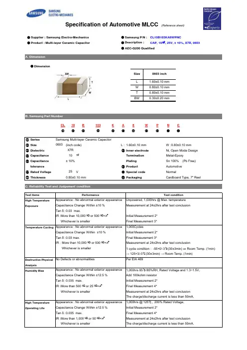
● Supplier : Samsung Electro-Mechanics CL10B103KA8WPNC● Product : Multi-layer Ceramic CapacitorCAP, 10㎋, 25V, ± 10%, X7R, 0603● AEC-Q200 QualifiedA. Dimension● DimensionB. Samsung Part NumberCL 10B K A 8W P N C ①②③⑤⑥⑦⑧⑨⑩⑪①Series Samsung Multi-layer Ceramic Capacitor ②Size (inch code)L :1.60±0.10 mm W :0.80±0.10 mm ③Dielectric ⑧Inner electrode Ni, Open Mode Design ④Capacitance ㎋Termination Metal-Epoxy ⑤Capacitance ± 10%Plating Sn 100% (Pb Free)tolerance ⑨Product Automotive ⑥Rated Voltage V⑩Special code Normal⑦Thickness0.80±0.10 mm⑪PackagingCardboard Type, 7" ReelTest items High Temperature Appearance : No abnormal exterior appearance Unpowered,1,**********************ExposureCapacitance Change Within ±10 %Measurement at 24±2hrs after test conclusion Tan δ :0.03 max.IR :More than 10,000 ㏁ or 500 ㏁×㎌Initial Measurement 2* Whichever is smallerFinal Measurement 3*Temperature Cycling Appearance : No abnormal exterior appearance1,000CyclesCapacitance Change Within ±10 %Initial Measurement 2* Tan δ :0.03 max.Final Measurement 3*IR :More than 10,000 ㏁ or 500 ㏁×㎌Measurement at 24±2hrs after test conclusionWhichever is smaller1 cycle condition : -55+0/-3℃(30±3min) → Room Temp. (1min)→ 125+3/-0℃(30±3min) → Room Temp. (1min)Destructive Physical No Defects or abnormalities Per EIA 469Analysis Humidity BiasAppearance : No abnormal exterior appearance 1,000hrs 85℃/85%RH, Rated Voltage and 1.3~1.5V,Capacitance Change Within ±12.5 %Add 100kohm resistor Tan δ :0.035 max.Initial Measurement 2* IR :More than 500 ㏁ or 25 ㏁×㎌Final Measurement 4*Whichever is smallerMeasurement at 24±2hrs after test conclusion The charge/discharge current is less than 50mA.High Temperature Appearance : No abnormal exterior appearance 1,000hrs @ 125℃, 200% Rated Voltage,Operating LifeCapacitance Change Within ±12.5 %Initial Measurement 2* Tan δ :0.035 max.Final Measurement 4*IR :More than 1,000 ㏁ or 50 ㏁×㎌Measurement at 24±2hrs after test conclusion Whichever is smallerThe charge/discharge current is less than 50mA.Specification of Automotive MLCC (Reference sheet)103L W T ● Samsung P/N :● Description :0.30±0.20 mmBWSize 0603 inch 1.60±0.10 mm 0.80±0.10 mm 0.80±0.10 mm X7R PerformanceTest condition25④060310External VisualNo abnormal exterior appearance Microscope (´10)Physical Dimensions Within the specified dimensions Using The calipersMechanical ShockAppearance : No abnormal exterior appearance Three shocks in each direction should be applied along Capacitance Change Within ±10 % 3 mutually perpendicular axes of the test specimen (18 shocks)Tan δ, IR :Initial spec.Initial Measurement 2* Final Measurement 5*VibrationAppearance : No abnormal exterior appearance 5g's for 20min., 12cycles each of 3 orientations,Capacitance Change Within ±10 %Use 8"×5" PCB 0.031" Thick 7 secure points on one long side Tan δ, IR :Initial spec.and 2 secure points at corners of opposite sides. Parts mounted within 2" from any secure point. Test from 10~2,000㎐.Initial Measurement 2* Final Measurement 5*Resistance to Appearance : No abnormal exterior appearance preheating : 150℃ for 60~120 sec.Solder HeatCapacitance Change Within ±10 %Solder pot : 260±5℃, 10±1sec.Tan δ, IR :Initial spec.Initial Measurement 2* Final Measurement 3*ESDAppearance : No abnormal exterior appearance AEC-Q200-002 or ISO/DIS10605Capacitance Change Within ±10 %Initial Measurement 2* Tan δ, IR :Initial spec.Final Measurement 4*Solderability95% of the terminations is to be soldered a) Preheat at 155℃ for 4 hours, Immerse in solder for 5s at 245±5℃evenly and continuouslyb) Steam aging for 8 hours, Immerse in solder for 5s at 245±5℃c) Steam aging for 8 hours, Immerse in solder for 120s at 260±5℃solder : a solution ethanol and rosinElectrical Capacitance : Within specified tolerance *A capacitor prior to measuring the capacitance is heat treated at CharacterizationTan δ :0.025 max.150 +0/-10℃ for 1hour and maintained in ambient air for 24±2 hours IR(25℃) :More than 10,000 ㏁ or 500 ㏁×㎌The Capacitance / D.F. should be measured at 25℃,Whichever is smaller1 ㎑ ± 10%,1 ± 0.2 VrmsIR(125℃) More than 1,000 ㏁ or 10 ㏁×㎌I.R. should be measured with a DC voltage not exceeding Whichever is smallerRated Voltage @25℃, @125℃ for 60~120 sec.Dielectric StrengthDielectric Strength : 250% of the rated voltage for 1~5 seconds Board FlexAppearance : No abnormal exterior appearance Bending to the limit,3 ㎜ for 60 seconds 1*Capacitance Change Within ±10 %Initial Measurement 2*Final Measurement 5*Terminal Appearance : No abnormal exterior appearance 10 N, for 60 sec.Strength(SMD)Capacitance Change Within ±10 %Initial Measurement 2* Final Measurement 5*Beam Load Destruction value should be exceed 20 NBeam speed :0.5±0.05 ㎜/secTemperature X7RCharacteristicsFrom -55 ℃ to 125 ℃, Capacitance change should be within ±15%Reflow ( Reflow Peak Temperature : 260 +0/-5℃, 30sec. ), Meet IPC/JEDEC J-STD-020 D Standard*1 : The figure indicates typical specification. Please refer to individual specifications.*2 : Initial measurement : Perform a heat treatment at 150 +0/-10℃ for one hour after soldering process. and then let sit for 24±2 hours at room temperature. Perform the initial measurement.*3 : Final measurement : Let sit for 24±2 hours at room temperature after test conclusion, then measure.*4 : Final measurement : Perform a heat treatment at 150 +0/-10℃ for one hour after soldering process. and then let sit for 24±2 hours at room temperature. Perform the initial measurement.*5 : Final measurement : Let measure within 24 hours at room temperature after test conclusion.Product specifications included in the specifications are effective as of March 1, 2013. Please be advised that they are standard product specifications for reference only.We may change, modify or discontinue the product specifications without notice at any time. So, you need to approve the product specifications before placing an order.Should you have any question regarding the product specifications, please contact our sales personnel or application engineers.0.5msHalf sine4.7m/secPerformance Test conditionPeak value Duration Wave Velocity 1,500G● Disclaimer & Limitation of Use and ApplicationThe products listed in this Specification sheet are NOT designed and manufactured for any use and applications set forth below.Please note that any misuse of the products deviating from products specifications or information provided in this Spec sheet may cause serious property damages or personal injury.We will NOT be liable for any damages resulting from any misuse of the products, specifically including using the products for high reliability applications as listed below.If you have any questions regarding this 'Limitation of Use and Application', you should first contact our sales personnel or application engineers.① Aerospace/Aviation equipment② Medical equipment③ Military equipment④ Disaster prevention/crime prevention equipment⑤ Power plant control equipment⑥ Atomic energy-related equipment⑦ Undersea equipment⑧ Traffic signal equipment⑨ Data-processing equipment⑩ Electric heating apparatus, burning equipment⑪ Safety equipment⑫ Any other applications with the same as or similar complexity or reliability to the applications。
风华高科电容多层片式陶瓷电容0805 CG 104 J 500 N T1 2 3 4 5 6 71、尺寸2、介质种类3、标称电容量(PF)4、误差级别5、工作电压6、端头类别7、包装方式型号英寸毫米代码介质材料表示方法实际值代码误差表示方法实际电压标记端头材料标记包装0402 0.04*0.02 1.00*0.5 CG COG和NPO 100 10*100J ±5% 6R3 6.3V S 纯银T 编带0603 0.06*0.03 1.6*0.8 101 10*101G ±2% 100 10V C 纯铜 B 散装0805 0.08*0.05 2.00*1.25 102 10*102 C ±0.25PF 250 25V N 三层电镀1206 0.12*0.06 3.2*1.6 500 50V三星电容多层片式陶瓷电容CL 10 C 101 J B 8 N N N C1 2 3 4 5 6 7 8 9 10 11CL表示:多层陶瓷贴片电容2、尺寸3介质种类4、标称电容量(PF)5、误差级别6、工作电压7、厚度8端头类别型号英寸毫米代码介质材料表示方法实际值代码误差表示方法实际电压标记尺寸(mm)标记端头材料0402 0.04*0.02 1.00*0.5 CPRSTUL COGP2HR2HS2HT2HU2JS2L100 10*100 J ±5% R 4V 3 0.3 N 三层电镀0603 0.06*0.03 1.6*0.8 101 10*101 G ±2% Q 6.3V 4 0.50805 0.08*0.05 2.00*1.25 102 10*102 C ±0.25PF P 10V 89ACD0.8 0.9 0.650.851.001206 0.12*0.06 3.2*1.6 OALB 16V 25V 35V 50VAB Y F X X5RX7RX7SY5VX6SKMZ±10%±20%+80/-20%CDEFGHIJK100V200V250V350V500V630V1000V2000V3000V国巨(YAGEO)电容多层片式陶瓷电容CC ×××× × ×NPO ×BN ×××1 2 3 4 51、尺寸2、误差精度3、包装形式4、实际电压值5、标称电容量型号英制型号公制代码误差表示方法实际值代码电压代码实际值0201 0603 BCDFGJ±0.1PF±0.25PF±0.5PF±1%±2%±5%R 纸卷盘7inch 7 16V 100 10*1000402 1005 K 吸塑卷盘7inch 8 25V 101 10*101 0603 1608 P 纸卷盘13inch 9 50V 102 10*102 0805 2012 F 吸塑卷盘13inch1206 3216 C 散装1210 32251812 4532TDK贴片电容型号TDK贴片电容的参数识别C 2012 X7R 1H 104 K T系列名称体积材料电压容量误差包装0603=0201 CH 0J=6.3V C=0.25 T=卷带1005=0402 COG 1A=10V D=0.5 B=袋装1608=0603 JB 1C=16V J=5%2012=0805 JF 1E=25V K=10%3216=1206 X7R 1H=50V M=20%3225=1210 X5R 2A=100V Z=+80-20%4532=1812 Y5V 2E=250V5650=2220 2J=630V4520=1808 3A=1KV3D=2KV3F=3KV。
三星帖片电容规格对照表规格试例:CL 10 A 105 K Q 8 N N N C1 2 3 4 5 6 7 8 9 10 111:系列编码CL=积层电容2:尺寸编码英寸(毫米) 英寸(毫米) 英寸(毫米)0.3=0201(0603) 21=0805(2012) 42=1808(4520)0.5=0402(1005) 31=1206(3216) 43=1812(4532)10=0603(1608) 32=1210(3225) 55=2220(5750)3:电介质编码I类II类C=COG S=S2H L=S2L A=X5R F=Y5VP=P2H T=T2H B=X7R X=X6SR=R2H U=U2J4:电容编码以PF表示的电容,2个有效位加上零的数量.例如:106=10X106=10000000PF 对于<10PF,字母R表示小数点.例如;1R5=1.5PF 5:公差编码B=±0.1PF F=±1PF, ±1% K=±10%C=±0.25PF G=±2% M=±20%D=±0.5PF J=±5% Z=+80/-20%对于小于等于10PF的数值,F=±1PF对于大于10PF的数值,F=±1%.6:额定电压编码R=4V O=16V B=50V E=250V I=1000VQ=6.3V A=25V C=100V G=500V J=2000VP=10V L=35V D=200V H=630V K=3000V7:厚度编码3=0.30毫米A=0.65毫米M=1.15毫米I=2.00毫米Q=1.25毫米5=0.50毫米C=0.85毫米F=1.25毫米J=2.50毫米V=2.50毫米8=0.80毫米D=1.00毫米H=1.60毫米L=3.20毫米8:内电极/端子/电镀编码A=常规产品钯/银/镍屏蔽/锡100%N=常规产品镍/铜/镍屏蔽/锡100%G=常规产品铜/铜/镍屏蔽/锡100%L=常规产品镍/铜/镍屏蔽/锡100%9:产品编码A=阵列(2-元素) L=L1CC B=阵列(4-元素) N=常规C=高频P=自动10:特殊编码N=预留给未来用途11:包装编码B=散装O=纸板箱料带,10英寸料盘E=压花纸板箱,7英寸料盘P=散装箱D=纸板箱料带,13英寸料盘(10000CA) F=压花纸板。
三星0603 22uf电容规格书三星0603 22uf电容规格书的解读与应用一、引言在现代电子产品中,电容作为一种重要的被动元件,在电路中扮演着储存电荷、滤波、耦合等重要作用。
而三星0603 22uf电容规格书作为电容的一种,其规格书所包含的信息对于电子工程师和电子爱好者来说是至关重要的。
在本篇文章中,我们将深度解读三星0603 22uf电容规格书的内容,并探讨其在电路设计和应用中的重要性。
二、三星0603 22uf电容规格书的解读1. 产品型号:三星0603 22uf电容规格书所指代的产品型号为0603,22uf。
其中,0603代表了电容的封装尺寸,而22uf则代表了电容的容量大小。
理解这一点对于正确选型和应用至关重要。
2. 规格参数:在规格书中,通常包含了电容的电压值、容差、温度特性等重要参数。
在选型过程中,需要根据具体的电路要求和环境条件来选择合适的规格参数,以确保电路稳定性和性能。
3. 使用注意事项:在规格书中,也会包含一些使用注意事项和贮存条件,这些信息对于保证电容性能和寿命至关重要。
在使用和贮存过程中需要严格按照规格书要求进行操作。
三、三星0603 22uf电容在电路设计和应用中的重要性作为一种常见的电容型号,三星0603 22uf电容在电路设计和应用中扮演着重要的角色。
由于其封装尺寸小巧,适合于电子产品的迷你化设计,因此在手机、平板等智能设备中得到了广泛应用。
22uf的较大容量可以满足一些对电荷储存和稳压要求较高的电路,例如稳压电路、滤波电路等。
在电子产品设计中,正确选用和应用三星0603 22uf电容对于提高电路性能和稳定性具有重要意义。
四、对三星0603 22uf电容的个人观点和理解在我看来,三星0603 22uf电容作为一种电子元件,其规格书所包含的信息对于电子工程师和电子爱好者来说是非常重要的。
通过深入了解其规格书的内容,可以更好地应用于实际电路设计中,并确保电路工作的稳定性和性能。
三星电容编码识别欧阳引擎(2021.01.01)你看盘子的料号如下对比:CL 03 B 104 K Q 8 N N N C1 2 3 4 5 6 7 8 9 10 111 系列编码:CL=积层陶瓷电容2 尺寸编码03=0201(0603) 21=0805(2012) 42=1808(4520) 05=0402(1005) 31=1206(3216) 43=1812(4532) 10=0603(1608) 32=1210(3225) 55=2220(5750) 14=0504(1410) 01=0306(0816) 12=0508(1220) 3 介质I类 II类C=C0G S=S2H L=S2LP=P2H T=T2HR=R2H U=U2JA=X5R F=Y5VB=X7R X=X6S4 容量电容容量用三位数表示,前面两位为有效数字,第三位为有效数字后"O"的位数如:104 = 1 00000 (单位pF)如果中间一位为R 则表示"."如:4R7 = 4.7pF5 电容的误差:B=±0.1pf F=±1pf±1% K=±10%C=±0.25pf G=±2% M=±20%D=±0.5pf? J=±5% Z=+80/-20%6 额定电压R=4V O =16V B =50V E = 250V I = 1000VQ=6.3V A =25V C=100V G = 500V J = 2000VP =10V L =35V D =200V H = 630V K= 3000V7 厚度:3=0.30毫米 A=0.65毫米 M=1.15毫米 I=2.00毫米 Q=1.25毫米5=0.50毫米 C=0.85毫米 F=1.25毫米 J=2.50毫米 V=2.50毫米8=0.80毫米 D=1.00毫米 H=1.60毫米 L=3.20毫米8 内电极A=常规产品钯/银/镍屏蔽/锡 100%N=常规产品镍/铜/镍屏蔽/锡 100%G=常规产品铜/铜/镍屏蔽/锡 100%L=低侧面产品镍/铜/镍屏蔽/锡 100%9 产品编码A =阵列(2-元素) L =LICCB =阵列(4-元素) N =常规P =自动 C=高频10 特殊编码11 包装编码B=散装 O=纸版箱料带,10英寸料盘 E=压花纸版箱,7英寸料盘P=散装箱 D=纸版箱料带,13英寸料盘(10000ea) F=压花纸版箱,13英寸料盘C=纸版箱料带,7英寸料盘 L=纸版箱料带,13英寸料盘(15,000ea) S=压花纸版箱,10英寸料盘。
三星内存编号命名揭秘!三星内存编号揭秘(一)三星DDR内存颗粒的编号共分为四段数字或字母,19个部分组成。
请看下面的三星内存编号示意图,图中有A、B、CDE和F为四段数字或字母,而19部分则是指包含在A、B、CDE和F四段数字或字母组成的编号,主要对内存规格进行说明。
下面,就给大家分别解释。
首先来解释一下四段号码的大概含义。
A部分我想不用解释了吧,标明的是生产企业的名称——SAMSUNG。
B部分说明的是该内存模组的生产日期,以三个阿拉伯数字的形式表现。
其中第一个阿拉伯数字表明,生产的年份,后面两位数字表明是在该年的第XX周生产的。
例如,上图中的446就该表示该模组是在04年的第46周生产的。
如果三位数字是532,则表明该内存模组是05年第32周生产的。
C部分说明的是该内存的封装类型,由一个英文字母表示。
该部分将分别以T、U、N、V、G、Z几个字母来代表不同的封装类型。
其中T代表是TSOP2封装,U表示TOSP2(Lead-Free)封装,N表示sTSOP2封装,V表示sTOSP2(Lead-Free)封装,G表示FBGA封装,Z表示FBGA(Lead-Free)封装。
D部分说明是该内存模组的工作温度与功耗,由一个英文字母表示。
该部分将以C和L两个字母来表示该内存颗粒的不同工作温度与功耗。
其中C表示该内存模组为大众商用型内存,普通功耗,工作温度在0 °C~70 °C之间;L表示该内存模组也属于大众商业型,但却是低功耗,工作温度也在0 °C~70 °C之间。
这部分标注为L的模组,在笔记本内存中比较常见。
E部分说明的是该内存模组的频率和各项延迟(即CL-tRCD-tRP),由两个英文字母或数字组成。
该部分分别以A0、B0、A2、B3和CC这五个字母/数字组合来代表不同频率和延迟的DDR内存模组。
其中,A0代表该模组的工作做频率为DDR-200(100MHz),延迟为2-2-2;B0代表DDR 266(133MHz),延迟为2.5-3-3;A2代表DDRDDR 266(133MHz),延迟为2-3-3;B3代表DDR333(166MHz),延迟为2.5-3-3;CC代表DDR400(200MHz),延迟为3-3-3。