Watermarking Low Bit-rate Advanced Simple Profile MPEG-4 Bitstreams
- 格式:pdf
- 大小:91.21 KB
- 文档页数:4

SDG2000X Series Function/Arbitrary Waveform GeneratorWWW.SIGLENT .COMOverviewSIGLENT’s SDG2000X is a series of dual-channel function/arbitrary waveform generators with specifications of up to 120MHz maximum bandwidth, 1.2GSa/s sampling rate and 16-bit vertical resolution. The proprietary TrueArb & EasyPulse techniques help to solve the weaknesses inherent in traditional DDS generators when generating arbitrary, square and pulse waveforms. With advantages above, SDG2000X can provide users with a variety of high fidelity and low jitter signals, which can meet the growing requirements of complex and extensive applications.Key FeaturesDual-channel, 120MHz maximum bandwidth, 20Vpp maximumoutput amplitude, high fidelity output with 80dB dynamic range High-performance sampling system with 1.2GSa/s sampling rate and 16-bit vertical resolution. No detail in your waveforms will be lostInnovative TrueArb technology, based on a point-by-point architecture, supports any 8pts~8Mpts Arb waveform with a sampling rate in range of 1μSa/s~75MSa/sInnovative EasyPulse technology, capable of generating lower jitter Square or Pulse waveforms, brings a wide range and extremely high precision in pulse width and rise/fall times adjustmentPlenty of analog and digital modulation types: AM 、DSB-AM 、FM 、PM 、FSK 、ASK 、PSK and PWM Sweep and Burst function Harmonic function196 built-in arbitrary waveforms High precision Frequency Counter Standard interfaces: USB Host, USB Device (USBTMC ), LAN(VXI-11)Optional interface: GPIB4.3” touch screen display for easier operationWWW.SIGLENT .COMSDG2000X Series Function/Arbitrary Waveform GeneratorModels and Key SpecificationsCharacteristicsHigh-performance Sampling SystemBenefiting from a 1.2GSa/s and 16-bit sampling system, SDG2000X achieves extremely high accuracy performance in both time domain and amplitude, which results in more accurately reconstructed waveforms and lower distortion.SDG2000X Series Function/Arbitrary Waveform GeneratorWWW.SIGLENT .COMExcellent Analog Channel Performance输出白噪声测试获得的系统-3dB 带宽在120MHz 以上Capacity of outputting large signal at high frequency. Dual-channel, 20 Vpp amplitude can be guaranteed even @20 MHz.The bandwidth of analog channels proves to be greater than 120MHz, via doing a frequency response test with white noise.Low noise floor , improves signal-noise ratio.High fidelity sine output. Almost no spurious observed @60MHz, 0dBm.CharacteristicsWWW.SIGLENT .COMSDG2000X Series Function/Arbitrary Waveform GeneratorInnovative EasyPulse TechnologyInnovative TrueArb TechnologyThe Pulse width can be fine-tuned to the minimum of 16.3ns with the adjustment step as small as 100ps.The rise/fall times can be set independently to the minimum of 8.4ns at any frequency and to the maximum of 22.4s. The adjustment step is as small as 100 ps.When a Square/Pulse waveform is generated by DDS, there will be a one-clock-jitter if the sampling rate is not an integer-related multiple of the output frequency.SDG2000X EasyPulse technology successfully overcomes this weakness in DDS designs and helps to produce low jitter Square/Pulse waveforms.TrueArb generates arbitrary waveforms point by point, never skips any point so that it can reconstruct all the details of the waveform as defined.As with EasyPulse, TrueArb effectively overcomes the defect that DDSmay cause the one-clock-jitter in arbitrary waveforms.For arbitrary waveforms, TrueArb not only has all the advantages of traditional DDS, but also eliminates the probability that DDS may cause serious jitter anddistortion.SDG2000X Series Function/Arbitrary Waveform GeneratorWWW.SIGLENT .COMModulationSweep4.3” Touch Screen Display Arbitrary Waveform Software EasyWaveXBurstFrequency CounterCharacteristicsSDG2000X supports plenty of modulation types, such as AM, FM, PM, FSK, ASK, PSK, DSB-AM, and so on. The modulation source can be configured as “Internal” or “External”.SDG2000X supports two Sweep modes, “Linear” and “Log”. Two Sweep directions, “Up” and “Down” and three Sweep sources, “Internal”, “External” and “Manual”.EasyWaveX is an arbitrary waveform software platform that supports waveform creation and editing. It features manual drawing, as-well-as line, equation, and coordinate editing modes. It is also a convenient way for users to edit their own arbitrary waveforms.4.3” touch screen display, makes operation much more convenient.SDG2000X supports two Burst modes, “N cycle” and “Gated”. The Burst source can be configured as “Internal” , “External” or “Manual”High precision Frequency Counter with an input frequency range of0.1Hz~200MHz.WWW.SIGLENT .COMSDG2000X Series Function/Arbitrary Waveform GeneratorSpecificationsAll specifications apply to both channels. Unless otherwise stated, all specifications are not guaranteed unless the following conditions are met:• The generator is within calibration period of validity• The generator has been working continuously for at least 30 minutes at a specified temperature (18℃ ~ 28℃).SDG2000X Series Function/Arbitrary Waveform Generator SpecificationsNote 1: The specification will be divided by 2 while applied to a 50Ω load.SDG2000X Series Function/Arbitrary Waveform Generator SpecificationsSDG2000X Series Function/Arbitrary Waveform Generator SpecificationsSDG2000X Series Function/Arbitrary Waveform Generator SpecificationsOrdering InformationFacebook: SiglentTech。
第一章概述1.1 系统优化介绍900/1800MHzTDMA数字蜂窝移动通信系统(GSM)是一个集网络技术、数字程控交换技术、各种传输技术和无线技术等领域的综合性系统,具有以下特性:●网络复杂,实体众多,接口多样●无线性能受无线信号覆盖情况、信号质量好坏、无线接口参数的设置等多种因素的影响●由于用户终端的流动性,使业务量、信令流量具有不确定性以上特性决定了网络运行性能是不稳定的,当网络的性能达不到设计要求;或为了使系统在现有资源条件下,更好地发挥自身具有的服务能力,通常需要对网络进行全方位的优化。
本文主要针对爱立信GSM 900M系统来论述优化的步骤和方法。
1.2优化流程可以将网络优化过程大致分为三个阶段:(1)网络现行状态的调查(2)优化实施(3)优化总结1.2.1 网络现行状态的调查本阶段的主要工作包括:(1)收集地图(2)获取基站的工程技术资料(3)现行网络的组成和结构情况(4)网络现有问题信息(5)基站故障报告(6)采集CDD(7)MSC/VLR局数据采集(8)采集BSC话务统计报告(9)采集交换机统计数据(10)普查性的拨打测试和路测通过以上过程,掌握当前系统的第一手资料和运行状况。
经过对所获取信息的分析处理,产生以下结果:系统的CDD 表、基站的工程技术表初步的场强分布图和信号质量分析表无线话务统计报告交换机接通率报告针对几大重点考查无线指标,找出无线性能差的小区,并得出初步的分析结果;从MSC的统计报告中找出接通率差的呼叫类型和局向,做为下一步优化的重点。
以上结果结合本次优化目标,制订优化方案。
1.2.2优化实施执行上一阶段制订的优化方案,主要工作有:●小区参数调整●针对性的路测和CQT●局数据调整●天线调整●挂接信令仪表,重点突击接通率问题优化的实施是优化工作的核心,时间跨度比较长,而且是一个动态调整的过程。
在执行期间需要根据当前系统的状况来制订下一步方案,直到达到优化的目标。
1.2.3优化总结和分析阶段本阶段的主要工作是:●对优化过程所获得的资料进行归档整理。
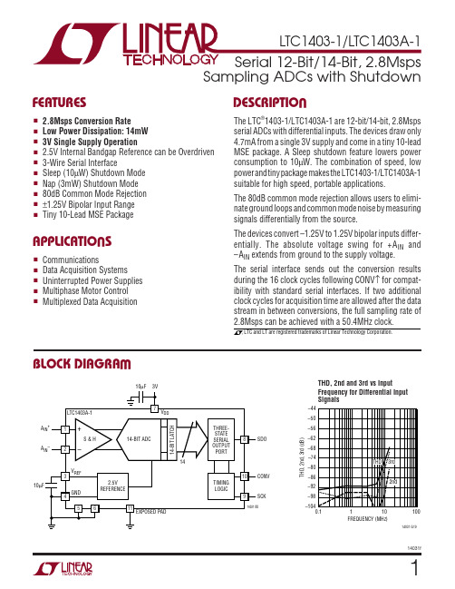
T JMAX = 125°C, θJA = 150°C/W EXPOSED PAD (PIN 11) IS GND MUST BE SOLDERED TO PCB12345A IN +A IN –V REF GND GND 109876CONV SCK SDO V DD GNDTOP VIEW11MSE PACKAGE10-LEAD PLASTIC MSOP (Notes 1, 2)Supply Voltage (V DD ).................................................4V Analog Input Voltage(Note 3)....................................–0.3V to (V DD + 0.3V)Digital Input Voltage ................... – 0.3V to (V DD + 0.3V)Digital Output Voltage..................–0.3V to (V DD + 0.3V)Power Dissipation..............................................100mW Operation Temperature RangeLTC1403C-1/LTC1403AC-1.....................0°C to 70°C LTC1403I-1/LTC1403AI-1..................–40°C to 85°C Storage Temperature Range.................–65°C to 150°C Lead Temperature (Soldering, 10 sec)..................300°CORDER PART NUMBERMSE PART MARKINGLTBGP LTBGQ LTBGR LTBGSLTC1403CMSE-1LTC1403IMSE-1LTC1403ACMSE-1LTC1403AIMSE-1The q denotes the specifications which apply over the full operatingtemperature range, otherwise specifications are at T A = 25°C. With internal reference. V DD = 3VLTC1403-1LTC1403A-1PARAMETERCONDITIONSMIN TYP MAXMIN TYP MAX UNITS Resolution (No Missing Codes)q 1214Bits Integral Linearity Error (Notes 4, 5, 18)q –2±0.252–4±0.54LSB Offset Error (Notes 4, 18)q –10±110–20±220LSB Gain Error (Note 4, 18)q–30±530–60±1060LSB Gain TempcoInternal Reference (Note 4)±15±15ppm/°C External Reference±1±1ppm/°CThe q denotes the specifications which apply over the full operating temperature range,otherwise specifications are at T A = 25°C. V DD = 3VSYMBOL PARAMETER CONDITIONS MIN TYP MAX UNITSV IN Analog Differential Input Range (Notes 3, 8, 9) 2.7V ≤ V DD ≤ 3.3Vq–1.25 to 1.25V V CM Analog Common Mode + Differential 0 to V DDVInput Range (Note 10)I IN Analog Input Leakage Current q 1µA C IN Analog Input Capacitance 13pF t ACQ Sample-and-Hold Acquisition Time (Note 6)q39ns t AP Sample-and-Hold Aperture Delay Time 1ns t JITTER Sample-and-Hold Aperture Delay Time Jitter 0.3ps CMRRAnalog Input Common Mode Rejection Ratiof IN = 1MHz, V IN = 0V to 3V –60dB f IN = 100MHz, V IN = 0V to 3V–15dBConsult LTC Marketing for parts specified with wider operating temperature ranges.ABSOLUTE AXI U RATI GSW W WU PACKAGE/ORDER I FOR ATIOU U WCO VERTER CHARACTERISTICSUA ALOG I PUTUU14031fThe q denotes the specifications which apply over the full operating temperature range,otherwise specifications are at T A = 25°C. V DD = 3V. Single-ended A IN + signal drive with A IN – = 1.5V DC. Differential signal drive with V CM = 1.5V at A IN + and A IN –LTC1403-1LTC1403A-1SYMBOL PARAMETER CONDITIONSMIN TYP MAX MIN TYP MAX UNITS SINADSignal-to-Noise Plus 100kHz Input Signal (Note 19)70.573.5dB Distortion Ratio1.4MHz Input Signal (Note 19)q6870.57073.5dB 100kHz Input Signal, External V REF = 3.3V,7276.3dB V DD ≥ 3.3V (Note 19)750kHz Input Signal, External V REF = 3.3V,7276.3dB V DD ≥ 3.3V (Note 19)THD Total Harmonic 100kHz First 5 Harmonics (Note 19)–87–90dB Distortion 1.4MHz First 5 Harmonics (Note 19)q –83–76–86–78dB SFDR Spurious Free 100kHz Input Signal (Note 19)–87–90dB Dynamic Range 1.4MHz Input Signal (Note 19)–83–86dB IMDIntermodulation 0.625V P-P 1.4MHz Summed with 0.625V P-P –82–82dB Distortion 1.56MHz into A IN + and Inverted into A IN –Code-to-Code V REF = 2.5V (Note 18)0.251LSB RMSTransition Noise Full Power Bandwidth V IN = 2.5V P-P , SDO = 11585LSB P-P (Note 15)5050MHz Full Linear BandwidthS/(N + D) ≥ 68dB55MHzThe q denotes the specifications which apply over thefull operating temperature range, otherwise specifications are at T A = 25°C. V DD = 3VPARAMETER CONDITIONS MINTYP MAXUNITSV REF Output Voltage I OUT = 02.5V V REF Output Tempco 15ppm/°C V REF Line Regulation V DD = 2.7V to 3.6V, V REF = 2.5V 600µV/V V REF Output Resistance Load Current = 0.5mA0.2ΩV REF Settling Time2msThe q denotes the specifications which apply over thefull operating temperature range, otherwise specifications are at T A = 25°C. V DD = 3VSYMBOL PARAMETERCONDITIONS MINTYP MAX UNITSV IH High Level Input Voltage V DD = 3.3V q 2.4V V IL Low Level Input Voltage V DD = 2.7V q 0.6V I IN Digital Input Current V IN = 0V to V DD q±10µA C IN Digital Input Capacitance (Note 20)5pF V OH High Level Output Voltage V DD = 3V, I OUT = –200µA q 2.5 2.9V V OL Low Level Output Voltage V DD = 2.7V, I OUT = 160µA 0.05V V DD = 2.7V, I OUT = 1.6mA q 0.100.4V I OZ Hi-Z Output Leakage D OUT V OUT = 0V to V DDq±10µA C OZ Hi-Z Output Capacitance D OUT 1pF I SOURCE Output Short-Circuit Source Current V OUT = 0V, V DD = 3V 20mA I SINKOutput Short-Circuit Sink CurrentV OUT = V DD = 3V 15mADY A IC ACCURACYUW I TER AL REFERE CE CHARACTERISTICSU U UDIGITAL I PUTS A D DIGITAL OUTPUTSUUSYMBOL PARAMETERCONDITIONSMIN TYP MAXUNITS f SAMPLE(MAX)Maximum Sampling Frequency per Channel q 2.8MHz (Conversion Rate)t THROUGHPUT Minimum Sampling Period (Conversion + Acquisiton Period)q357ns t SCK Clock Period (Note 16)q19.810000nst CONV Conversion Time(Note 6)1618SCLK cyclest 1Minimum Positive or Negative SCLK Pulse Width (Note 6)2ns t 2CONV to SCK Setup Time(Notes 6, 10)3ns t 3Nearest SCK Edge Before CONV(Note 6)0ns t 4Minimum Positive or Negative CONV Pulse Width (Note 6)4ns t 5SCK to Sample Mode (Note 6)4ns t 6CONV to Hold Mode(Notes 6, 11) 1.2ns t 716th SCK ↑ to CONV ↑ Interval (Affects Acquisition Period)(Notes 6, 7, 13)45ns t 8Minimum Delay from SCK to Valid Data (Notes 6, 12)8ns t 9SCK to Hi-Z at SDO(Notes 6, 12)6ns t 10Previous SDO Bit Remains Valid After SCK(Notes 6, 12)2ns t 12V REF Settling Time After Sleep-to-Wake Transition(Notes 6, 14)2msTI I G CHARACTERISTICSWU The q denotes the specifications which apply over the full operating temperaturerange, otherwise specifications are at T A = 25°C. V DD = 3VPOWER REQUIRE E T SWU The q denotes the specifications which apply over the full operating temperaturerange, otherwise specifications are at T A = 25°C. (Note 17)SYMBOL PARAMETER CONDITIONSMIN TYP MAX UNITSV DD Supply Voltage2.73.6V I DDPositive Supply VoltageActive Mode q 4.77mA Nap Modeq1.1 1.5mA Sleep Mode (LTC1403)215µA Sleep Mode (LTC1403A)210µA P DPower DissipationActive Mode with SCK in Fixed State (Hi or Lo)12mWNote 1: Absolute Maximum Ratings are those values beyond which the life of a device may be impaired.Note 2: All voltage values are with respect to GND.Note 3: When these pins are taken below GND or above V DD , they will be clamped by internal diodes. This product can handle input currents greater than 100mA below GND or greater than V DD without latchup.Note 4: Offset and full-scale specifications are measured for a single-ended A IN + input with A IN – grounded and using the internal 2.5V reference.Note 5: Integral linearity is tested with an external 2.55V reference and is defined as the deviation of a code from the straight line passing through the actual endpoints of a transfer curve. The deviation is measured from the center of quantization band.Note 6: Guaranteed by design, not subject to test.Note 7: Recommended operating conditions.Note 8: The analog input range is defined for the voltage differencebetween A IN + and A IN –. Performance is specified with A IN – = 1.5V DC while driving A IN +.Note 9: The absolute voltage at A IN + and A IN – must be within this range.Note 10: If less than 3ns is allowed, the output data will appear one clock cycle later. It is best for CONV to rise half a clock before SCK, when running the clock at rated speed.Note 11: Not the same as aperture delay. Aperture delay is smaller (1ns)because the 2.2ns delay through the sample-and-hold is subtracted from the CONV to Hold mode delay.Note 12: The rising edge of SCK is guaranteed to catch the data coming out into a storage latch.Note 13: The time period for acquiring the input signal is started by the 16th rising clock and it is ended by the rising edge of convert.Note 14: The internal reference settles in 2ms after it wakes up from Sleep mode with one or more cycles at SCK and a 10µF capacitive load.Note 15: The full power bandwidth is the frequency where the output code swing drops to 3dB with a 2.5V P-P input sine wave.Note 16: Maximum clock period guarantees analog performance during conversion. Output data can be read without an arbitrarily long clock.Note 17: V DD = 3V, f SAMPLE = 2.8Msps.Note 18: The LTC1403A-1 is measured and specified with 14-bitResolution (1LSB = 152µV) and the LTC1403-1 is measured and specified with 12-bit Resolution (1LSB = 610µV).Note 19: Full-scale sinewaves are fed into the noninverting input while the inverting input is kept at 1.5V DC.Note 20: The sampling capacitor at each input accounts for 4.1pF of the input capacitance.DRIVING THE ANALOG INPUTThe differential analog inputs of the LTC1403-1/LTC1403A-1are easy to drive. The inputs may be driven differentially or as a single-ended input (i.e., the A IN – input is set to V CM ). Both differential analog inputs, A IN + with A IN –, are sampled at the same instant. Any unwanted signal that is common to both inputs of each input pair will be reduced by the common mode rejection of the sample-and-hold circuit. The inputs draw only one small current spike while charging the sample-and-hold capacitors at the end of conversion. During conversion, the analog inputs draw only a small leakage current. If the source impedance of the driving circuit is low, then the LTC1403-1/LTC1403A-1 inputs can be driven directly. As source imped-ance increases, so will acquisition time. For minimum acqui-sition time with high source impedance, a buffer amplifier must be used. The main requirement is that the amplifier driving the analog input(s) must settle after the small current spike before the next conversion starts (settling time must be 39ns for full throughput rate). Also keep in mind while choosing an input amplifier, the amount of noise and har-monic distortion added by the amplifier.CHOOSING AN INPUT AMPLIFIERChoosing an input amplifier is easy if a few requirements are taken into consideration. First, to limit the magnitude of the voltage spike seen by the amplifier from charging the sam-pling capacitor, choose an amplifier that has a low output impedance (<100Ω) a t t he c losed-loop b andwidth f requency.For example, if an amplifier is used with a gain of 1 and has a unity-gain bandwidth of 50MHz, then the output impedance at 50MHz must be less than 100Ω. The second requirement is that the closed-loop bandwidth must be greater than 40MHz to ensure adequate small-signal settling for full throughput rate. If slower op amps are used, more time for settling can be provided by increasing the time between conversions. The best choice for an op amp to drive the LTC1403-1/LTC1403A-1 w ill d epend o n t he a pplication. G en-erally, applications fall into two categories: AC applications where dynamic specifications are most critical and time domain applications where DC accuracy and settling time are most critical. The following list is a summary of the op amps that are suitable for driving the LTC1403-1/LTC1403A-1.(More detailed information is available in the Linear Technol-ogy Databooks and our website at .)LTC ®1566-1: Low Noise 2.3MHz Continuous Time Low-Pass Filter.LT1630: Dual 30MHz Rail-to-Rail Voltage FB Amplifier. 2.7V to ±15V supplies. Very high A VOL , 500µV offset and 520ns settling to 0.5LSB for a 4V swing. THD and noise are –93dB to 40kHz and below 1LSB to 320kHz (A V = 1, 2V P-P into 1k Ω,V S = 5V), making the part excellent for AC applications (to 1/3 Nyquist) where rail-to-rail performance is desired. Quad version is available as LT1631.LT1632: Dual 45MHz Rail-to-Rail Voltage FB Amplifier. 2.7V to ±15V supplies. Very high A VOL , 1.5mV offset and 400ns settling to 0.5LSB for a 4V swing. It is suitable for applica-tions with a single 5V supply. THD and noise are –93dB to 40kHz and below 1LSB to 800kHz (A V = 1,2V P-P into 1k Ω, V S = 5V), making the part excellent for AC applications where rail-to-rail performance is desired. Quad version is available as LT1633.LT1813: Dual 100MHz 750V/µs 3mA Voltage Feedback Amplifier. 5V to ±5V supplies. Distortion is –86dB to 100kHz and –77dB to 1MHz with ±5V supplies (2V P-P into 500Ω).Excellent part for fast AC applications with ±5V␣supplies.LT1801: 80MHz GBWP, –75dBc at 500kHz, 2mA/Amplifier,8.5nV/√Hz.LT1806/LT1807: 325MHz G BWP, –80dBc D istortion a t 5MHz,Unity-Gain S table, R -R I n a nd O ut, 10mA/Amplifier, 3.5nV/√Hz.LT1810: 180MHz GBWP, –90dBc Distortion at 5MHz,Unity-Gain S table, R -R I n a nd O ut, 15mA/Amplifier, 16nV/√Hz.LT1818/LT1819: 400MHz, 2500V/µs,9mA, Single/Dual Volt-age Mode Operational Amplifier.LT6200: 165MHz GBWP, –85dBc Distortion at 1MHz, Unity-Gain Stable, R-R In and Out, 15mA/Amplifier,0.95nV/√Hz.LT6203: 100MHz GBWP, –80dBc Distortion at 1MHz,Unity-Gain Stable, R-R In and Out, 3mA/Amplifier,1.9nV/√Hz.LT6600-10: Amplifier/Filter Differential In/Out with 10MHz Cutoff.APPLICATIO S I FOR ATIOW UUU111214031 F07Figure 7. Recommended LayoutDigital circuitry grounds must be connected to the digital supply common. In applications where the ADC data outputs and control signals are connected to a continu-ously active microprocessor bus, it is possible to get errors in the conversion results. These errors are due to feedthrough from the microprocessor to the successive131414031fmode and the power drain drops from 14mW to 6mW. The internal reference remains powered in Nap mode. One or more rising edges at SCK wake up the LTC1403-1/LTC1403A-1 for service very quickly, and CONV can start an accurate conversion within a clock cycle. Four rising edges at CONV, without any intervening rising edges at SCK, put the LTC1403-1/LTC1403A-1 in Sleep mode and the power drain drops from 16mW to 10µW. One or more rising edges at SCK wake up the LTC1403-1/LTC1403A-1for operation. The internal reference (V REF ) takes 2ms to slew and settle with a 10µF load. Note that, using sleep mode more frequently than every 2ms, compromises the settled accuracy of the internal reference. Note that, for slower conversion rates, the Nap and Sleep modes can be used for substantial reductions in power consumption.DIGITAL INTERFACEThe LTC1403-1/LTC1403A-1 has a 3-wire SPI (Serial Protocol Interface) interface. The SCK and CONV inputs and SDO output implement this interface. The SCK and CONV inputs accept swings from 3V logic and are TTL compatible, if the logic swing does not exceed V DD . A detailed description of the three serial port signals follows:Conversion Start Input (CONV)The rising edge of CONV starts a conversion, but subse-quent rising edges at CONV are ignored by the LTC1403-1/LTC1403A-1 until the following 16 SCK rising edges have occurred. It is necessary to have a minimum of 16 rising edges of the clock input SCK between rising edges of CONV. But to obtain maximum conversion speed, it is necessary to allow two more clock periods between con-versions to allow 39ns of acquisition time for the internal ADC sample-and-hold circuit. With 16 clock periods per conversion, the maximum conversion rate is limited to 2.8Msps to allow 39ns for acquisition time. In either case,the output data stream comes out within the first 16 clock periods to ensure compatibility with processor serial ports. The duty cycle of CONV can be arbitrarily chosen to be used as a frame sync signal for the processor serial port. A simple approach to generate CONV is to create a pulse that is one SCK wide to drive the LTC1403-1/LTC1403A-1 and then buffer this signal with the appropri-ate number of inverters to ensure the correct delay drivingthe frame sync input of the processor serial port. It is good practice to drive the LTC1403-1/LTC1403A-1 CONV input first to avoid digital noise interference during the sample-to-hold transition triggered by CONV at the start of conver-sion. It is also good practice to keep the width of the low portion of the CONV signal greater than 15ns to avoid introducing glitches in the front end of the ADC just before the sample-and-hold goes into hold mode at the rising edge of CONV.Minimizing Jitter on the CONV InputIn high speed applications where high amplitude sinewaves above 100kHz are sampled, the CONV signal must have as little jitter as possible (10ps or less). The square wave output of a common crystal clock module usually meets this requirement easily. The challenge is to generate a CONV signal from this crystal clock without jitter corrup-tion from other digital circuits in the system. A clock divider and any gates in the signal path from the crystal clock to the CONV input should not share the same integrated circuit with other parts of the system. As shown in the interface circuit examples, the SCK and CONV inputs should be driven first, with digital buffers used to drive the serial port interface. Also note that the master clock in the DSP may already be corrupted with jitter, even if it comes directly from the DSP crystal. Another problem with high speed processor clocks is that they often use a low cost,low speed crystal (i.e., 10MHz) to generate a fast, but jittery, phase-locked-loop system clock (i.e., 40MHz). The jitter in these PLL-generated high speed clocks can be several nanoseconds. Note that if you choose to use the frame sync signal generated by the DSP port, this signal will have the same jitter of the DSP’s master clock.Serial Clock Input (SCK)The rising edge of SCK advances the conversion process and also udpates each bit in the SDO data stream. After CONV rises, the third rising edge of SCK starts clocking out the 12/14 data bits with the MSB sent first. A simple approach is to generate SCK to drive the LTC1403-1/LTC1403A-1 first and then buffer this signal with the appropriate number of inverters to drive the serial clock input of the processor serial port. Use the falling edge of the clock to latch data from the Serial Data Output (SDO)APPLICATIO S I FOR ATIOW UUU151614031fAPPLICATIO S I FOR ATIOW UU U ; 10-23-03 ******************************************************************; Files: 014SI.ASM -> 1403 bipolar Sine wave collection with Serial Port interface ; bvectors.asm buffered mode.; s2k14ini.asm 2k buffer size.; first element at 1024, last element at 1023, two middles at 2047 and 0000; bipolar mode; Works 16 or 64 clock frames.; negative edge BCLKR ; negative BFSR pulse ; -0 data shifted; 1' cable from counter to CONV at DUT ; 2' cable from counter to CLK at DUT; *************************************************************************** .width 160 .length 110.title “sineb0 BSP in auto buffer mode” .mmregs.setsect “.text”, 0x500,0 ;Set address of executable.setsect “vectors”, 0x180,0 ;Set address of incoming 1403 data.setsect “buffer”, 0x800,0 ;Set address of BSP buffer for clearing .setsect “result”, 0x1800,0 ;Set address of result for clearing .text ;.text marks start of codestart:;this label seems necessary;Make sure /PWRDWN is low at J1-9 ;to turn off AC01 adc tim=#0fh prd=#0fhtcr = #10h ; stop timertspc = #0h ; stop TDM serial port to AC01pmst = #01a0h ; set up iptr. Processor Mode STatus register sp = #0700h ; init stack pointer. dp = #0 ; data pagear2 = #1800h ; pointer to computed receive buffer.ar3 = #0800h ; pointer to Buffered Serial Port receive buffer ar4 = #0h ; reset record countercall sineinit ; Double clutch the initialization to insure a proper sinepeek:call sineinit ; reset. The external frame sync must occur 2.5 clocks ; or more after the port comes out of reset.wait goto wait; ————————Buffered Receive Interrupt Routine —————————breceive:ifr = #10h ; clear interrupt flagsTC = bitf(@BSPCE,#4000h) ; check which half (bspce(bit14)) of buffer if (NTC) goto bufull ; if this still the first half get next half bspce = #(2023h + 08000h); turn on halt for second half (bspce(bit15)) return_enable; ———————mask and shift input data ——————————————bufull:b = *ar3+ << -0 ; load acc b with BSP buffer and shift right -0 b = #03FFFh & b ; mask out the TRISTATE bits with #03FFFhb = b ^ #2000h ; invert the MSB for bipolar operation B *ar2+ = data(#0bh) ; store B to out buffer and advance AR2 pointer TC = (@ar2 == #02000h) ; output buffer is 2k starting at 1800h if (TC) goto start ; restart if out buffer is at 1fffh goto bufull1714031fAPPLICATIO S I FOR ATIOW UU U ; —————————dummy bsend return————————————bsend return_enable ;this is also a dummy return to define bsend ;in vector table file BVECTORS.ASM ; ——————————— end ISR ——————————————.copy “c:\dskplus\1403\s2k14ini.asm” ;initialize buffered serial port .space 16*32 ;clear a chunk at the end to mark the end ;======================================================================;; VECTORS ;;====================================================================== .sect “vectors” ;The vectors start here .copy “c:\dskplus\1403\bvectors.asm” ;get BSP vectors.sect “buffer” ;Set address of BSP buffer for clearing .space 16*0x800.sect “result” ;Set address of result for clearing .space 16*0x800 .end; ***************************************************************************; File: BVECTORS.ASM -> Vector Table for the ‘C54x DSKplus 10.Jul.96; BSP vectors and Debugger vectors ; TDM vectors just return; ***************************************************************************; The vectors in this table can be configured for processing external and ; internal software interrupts. The DSKplus debugger uses four interrupt ; vectors. These are RESET, TRAP2, INT2, and HPIINT.; * DO NOT MODIFY THESE FOUR VECTORS IF YOU PLAN TO USE THE DEBUGGER *;; All other vector locations are free to use. When programming always be sure ; the HPIINT bit is unmasked (IMR=200h) to allow the communications kernel and ; host PC interact. INT2 should normally be masked (IMR(bit 2) = 0) so that the ; DSP will not interrupt itself during a HINT. HINT is tied to INT2 externally.;;;.title “Vector Table” .mmregsreset goto #80h ;00; RESET * DO NOT MODIFY IF USING DEBUGGER * nop nopnmi return_enable ;04; non-maskable external interrupt nop nop noptrap2 goto #88h ;08; trap2 * DO NOT MODIFY IF USING DEBUGGER * nop nop.space 52*16 ;0C-3F: vectors for software interrupts 18-30int0 return_enable ;40; external interrupt int0 nop nop nopint1 return_enable ;44; external interrupt int1 nop nop nop1814031fAPPLICATIO S I FOR ATIOW UUU int2 return_enable ;48; external interrupt int2 nop nop noptint return_enable ;4C; internal timer interrupt nop nop nopbrint goto breceive ;50; BSP receive interrupt nop nop nopbxint goto bsend ;54; BSP transmit interrupt nop nop noptrint return_enable ;58; TDM receive interrupt nop nop noptxint return_enable ;5C; TDM transmit interrupt nop nopint3 return_enable ;60; external interrupt int3 nop nop nophpiint dgoto #0e4h ;64; HPIint * DO NOT MODIFY IF USING DEBUGGER * nop nop.space 24*16 ;68-7F; reserved area*********************************************************************** (C) COPYRIGHT TEXAS INSTRUMENTS, INC. 1996 ************************************************************************ ** File: s2k14ini.ASM BSP initialization code for the ‘C54x DSKplus ** for use with 1403 in buffered mode ** BSPC and SPC are the same in the ‘C542 ** BSPCE and SPCE seem the same in the ‘C542 *********************************************************************** .title “Buffered Serial Port Initialization Routine”ON .set 1OFF .set !ON YES .set 1NO .set !YES BIT_8 .set 2BIT_10 .set 1BIT_12 .set 3BIT_16 .set 0GO .set 0x80*********************************************************************** This is an example of how to initialize the Buffered Serial Port (BSP).* The BSP is initialized to require an external CLK and FSX for* operation. The data format is 16-bits, burst mode, with autobuffering * enabled.*1914031fAPPLICATIO S I FOR ATIOW UUU ******************************************************************************************************LTC1403 timing from board with 10MHz crystal.**10MHz, divided from 40MHz, forced to CLKIN by 1403 board. **Horizontal scale is 25ns/chr or 100ns period at BCLKR **Timing measured at DSP pins. Jxx pin labels for jumper cable. **BFSR Pin J1-20 ~~\____/~~~~~~~~~~~~~~~~~~~~~~~~~~~~~~~~~~~~~~~~~~~~~~~~~~~~~~~~~~\____/~~~~~~~~~~~**BCLKR Pin J1-14 _/~\_/~\_/~\_/~\_/~\_/~\_/~\_/~\_/~\_/~\_/~\_/~\_/~\_/~\_/~\_/~\_/~\_/~\_/~\_/~\_/~**BDR Pin J1-26 _—_—_—<B13-B12-B11-B10-B09-B08-B07-B06-B05-B04-B03-B02-B01-B00>—_—<B13-B12**CLKIN Pin J5-09 ~~~~~\_______/~~~~~~~\_______/~~~~~~~\_______/~~~~~~~\_______/~~~~~~~\_______/~~~~~**C542 read 0 B13 B12 B11 B10 B09 B08 B07 B06 B05 B04 B03 B02 B01 B00 0 0 B13 B12** ** negative edge BCLKR * negative BFSR pulse * no data shifted* 1' cable from counter to CONV at DUT * 2' cable from counter to CLK at DUT*No right shift is needed to right justify the input data in the main program **the two msbs should also be masked *******************************************************************************************************Loopback .set NO ;(digital looback mode?) DLB bit Format .set BIT_16 ;(Data format? 16,12,10,8) FO bit IntSync .set NO ;(internal Frame syncs generated?) TXM bit IntCLK .set NO ;(internal clks generated?) MCM bit BurstMode .set YES ;(if BurstMode=NO, then Continuous) FSM bit CLKDIV .set 3 ;(3=default value, 1/4 CLOCKOUT)PCM_Mode .set NO ;(Turn on PCM mode?)FS_polarity .set YES ;(change polarity)YES=^^^\_/^^^, NO=___/^\___CLK_polarity .set NO ;(change polarity)for BCLKR YES=_/^, NO=~\_Frame_ignore .set !YES ;(inverted !YES -ignores frame)XMTautobuf .set NO ;(transmit autobuffering)RCVautobuf .set YES ;(receive autobuffering)XMThalt .set NO ;(transmit buff halt if XMT buff is full)RCVhalt .set NO ;(receive buff halt if RCV buff is full)XMTbufAddr .set 0x800 ;(address of transmit buffer)XMTbufSize .set 0x000 ;(length of transmit buffer)RCVbufAddr .set 0x800 ;(address of receive buffer)RCVbufSize .set 0x800 ;(length of receive buffer)works up to 800** See notes in the ‘C54x CPU and Peripherals Reference Guide on setting up * valid buffer start and length values. Page 9-44************************************************************************.eval ((Loopback >> 1)|((Format & 2)<<1)|(BurstMode <<3)|(IntCLK <<4)|(IntSync <<5)) ,SPCval .eval ((CLKDIV)|(FS_polarity <<5)|(CLK_polarity<<6)|((Format &1)<<7)|(Frame_ignore<<8)|(PCM_Mode<<9)), SPCEval.eval (SPCEval|(XMTautobuf<<10)|(XMThalt<<12)|(RCVautobuf<<13)|(RCVhalt<<15)), SPCEval sineinit:bspc = #SPCval ; places buffered serial port in reset ifr = #10h ; clear interrupt flagsimr = #210h ; Enable HPINT,enable BRINT0intm = 0 ; all unmasked interrupts are enabled. bspce = #SPCEval ; programs BSPCE and ABUaxr = #XMTbufAddr ; initializes transmit buffer start address bkx = #XMTbufSize ; initializes transmit buffer sizearr = #RCVbufAddr ; initializes receive buffer start address bkr = #RCVbufSize ; initializes receive buffer sizebspc = #(SPCval | GO) ; bring buffered serial port out of reset return ;for transmit and receive because GO=0xC0Information furnished by Linear Technology Corporation is believed to be accurate and reliable.However, no responsibility is assumed for its use. Linear Technology Corporation makes no represen-tation that the interconnection of its circuits as described herein will not infringe on existing patent rights.。

1Introduction1.1Features1.2APPLICATIONS1.3DescriptionTRF7960,TRF7961MULTI-STANDARD FULLY INTEGRATED 13.56-MHZ RFID ANALOG FRONT END AND DATA-FRAMING READER SYSTEMSLOU186E–AUGUST 2006–REVISED JULY 2008–Standby 120µA•Completely Integrated Protocol Handling–Active (Rx only)10mA•Separate Internal High-PSRR Power Supplies •Parallel 8-Bit or Serial 4-Pin SPI Interface With for Analog,Digital,and PA Sections Provide MCU Using 12-Byte FIFONoise Isolation for Superior Read Range and Reliability•Ultrasmall 32-Pin QFN Package (5mm ×5mm)•Dual Receiver Inputs With AM and PM•Available ToolsDemodulation to Minimize Communication –Reference Design/EVM With Development HolesSoftware•Receiver AM and PM RSSI–Source Code Available for MSP430•Reader-to-Reader Anti-Collision•High Integration Reduces Total BOM and Board Area•Secure Access Control –Single External 13.56-MHz Crystal Oscillator•Product Authentication –MCU-Selectable Clock-Frequency Output of –Printer Ink Cartridges RF,RF/2,or RF/4–Blood Glucose Monitors –Adjustable 20-mA,High-PSRR LDO for •Contactless Payment Systems Powering External MCU•Medical Systems•Easy to Use With High Flexibility–Auto-Configured Default Modes for Each Supported ISO Protocol–12User-Programmable Registers The TRF7960/61is an integrated analog front –Selectable Receiver Gain and AGC end and data-framing system for a 13.56-MHz –Programmable Output Power RFID reader system.Built-in programming (100mW or 200mW)options make it suitable for a wide range of –Adjustable ASK Modulation Range applications for proximity and vicinity RFID (8%to 30%)systems.–Built-In Receiver Band-Pass Filter With User-Selectable Corner FrequenciesThe reader is configured by selecting the •Wide Operating Voltage Range of 2.7V to 5.5V desired protocol in the control registers.Direct •Ultralow-Power Modes access to all control registers allows fine tuning –Power Down <1µAof various reader parameters as needed.Table 1-1.PRODUCT SELECTION TABLEPROTOCOLSDEVICEISO14443A/BISO15693Tag-it™ISO18000-3106kbps212kbps424kbps848kbpsTRF7960√√√√√√TRF7961√√Please be aware that an important notice concerning availability,standard warranty,and use in critical applications of Texas Instruments semiconductor products and disclaimers thereto appears at the end of this document.Tag-it is a trademark of Texas Instruments Incorporated.PRODUCTION DATA information is current as of publication date.Copyright ©2006–2008,Texas Instruments IncorporatedProducts conform to specifications per the terms of the Texas Instruments standard warranty.Production processing does not necessarily include testing of all parameters.ContentsTRF7960,TRF7961MULTI-STANDARD FULLY INTEGRATED 13.56-MHZ RFIDANALOG FRONT END AND DATA-FRAMING READER SYSTEMSLOU186E–AUGUST 2006–REVISED JULY 20084.4.1Application Schematic for the TRF7960EVM1Introduction ...............................................(Parallel Mode).......................................1.1Features ..............................................4.4.2ApplicationSchematicfortheTRF7961EVM(SPI1.2APPLICATIONS......................................Mode).................................................1.3Description (5)System Description ....................................2Description (continued)................................ 5.1Power Supplies .. (3)Physical Characteristics ............................... 5.2Receiver –Analog Section ..........................3.1Terminal Functions ................................... 5.3Register Descriptions ................................3.1PACKAGING/ORDERING INFORMATION..........5.4Direct Commands From MCU to Reader...........4ELECTRICAL SPECIFICATIONS ...................... 5.5Reader Communication Interface ...................4.1ABSOLUTE MAXIMUM RATINGS ................... 5.6Parallel Interface Communication ...................4.2DISSIPATION RATINGS TABLE .................... 5.7Serial Interface Communication .....................4.3RECOMMENDED OPERATING CONDITIONS ...... 5.8External Power Amplifier Application ................4.4ELECTRICAL CHARACTERISTICS .................2Contents Submit Documentation Feedback2Description (continued)TRF7960,TRF7961MULTI-STANDARD FULLY INTEGRATED 13.56-MHZ RFID ANALOG FRONT END AND DATA-FRAMING READER SYSTEMSLOU186E–AUGUST 2006–REVISED JULY 2008Figure 2-1.Typical ApplicationA parallel or serial interface can be used for communication between the MCU and reader.When hardware encoders and decoders are used (accelerators for different standards),transmit and receive functions use a 12-byte FIFO register.For direct transmit or receive functions,the encoders/decoders can be bypassed so the MCU can process the data in real time.The transmitter has selectable output-power levels of 100mW (20dBm)or 200mW (23dBm)into a 50-Ωload (at 5-V supply)and is capable of ASK or OOK modulation.Integrated voltage regulators ensure power-supply noise rejection for the complete reader system.Data transmission comprises low-level encoding for ISO15693,modified Miller for ISO14443-A,high-bit-rate systems and Tag-it coding systems.Included with the data encoding is automatic generation of SOF,EOF,CRC,and/or parity bits.The receiver system enables AM and PM demodulation using a dual-input architecture.The receiver also includes an automatic gain control option and selectable gain.Also included is a selectable bandwidth to cover a broad range of input subcarrier signal options.The received signal strength for AM and PM modulation is accessible via the RSSI register.The receiver output is selectable among a digitized subcarrier signal and any of ten integrated subcarrier decoders (two for ISO15693low bit rate,two for ISO15693high bit rate,two for ISO14443,three for ISO14443high bit rates and one for Tag-it systems).Selected decoders also deliver bit stream and a data clock as outputs.The receiver system also includes a framing system.This system performs the CRC and/or parity check,removes the EOF and SOF settings,and organizes the data in bytes.Framed data is then accessible to the MCU via a 12-byte FIFO register and MCU interface.The framing supports ISO14443and ISO15693protocols.The TRF7960/61supports data communication levels from 1.8V to 5.5V for the MCU I/O interface while also providing a data synchronization clock.An auxiliary 20-mA regulator (pin 32)is available for additional system circuits.Submit Documentation Feedback Description (continued)33Physical Characteristics3.1Terminal Functions242322212019181723456781109116151413123231302928272625TRF7960,TRF7961MULTI-STANDARD FULLY INTEGRATED 13.56-MHZ RFIDANALOG FRONT END AND DATA-FRAMING READER SYSTEMSLOU186E–AUGUST 2006–REVISED JULY 2008Figure 3-1.TRF796x Pin Assignments (Top View)Table 3-1.Terminal FunctionsTERMINAL TYPE (1)DESCRIPTIONNAME NO.Also can be configured to provide the received analog signal output (ANA_OUT)ASK/OOK 12BID Direct mode,selection between ASK and OOK modulation (0=ASK,1=OOK)BAND_GAP 11OUT Band-gap voltage (1.6V);internal analog voltage reference;must be ac-bypassed to ground.DATA_CLK 26INP Clock input for MCU communication (parallel and serial)EN 28INP Chip enable input (If EN =0,then chip is in power-down mode).Pulse enable and selection of power down mode.If EN2is connected to VIN,then VDD_X is EN225INP active during power down to support the MCU.Pin can also be used for pulse wake-up from power-down mode.I/O_017BID I/O pin for parallel communication I/O_118BID I/O pin for parallel communication I/O_219BID I/O pin for parallel communication I/O_320BID I/O pin for parallel communication I/O_421BID I/O pin for parallel communication I/O pin for parallel communication I/O_522BIDStrobe out clock for serial communication Data clock output in direct mode I/O pin for parallel communicationI/O_623BIDMISO for serial communication (SPI)Serial bit data output in direct mode 1or subcarrier signal in direct mode 0I/O pin for parallel communication.I/O_724BID MOSI for serial communication (SPI)IRQ 13OUT Interrupt requestMOD 14INPDirect mode,external modulation input(1)SUP =Supply,INP =Input,BID =Bi-directional,OUT =OutputPhysical Characteristics4Submit Documentation Feedback3.1PACKAGING/ORDERING INFORMATION(1)TRF7960,TRF7961MULTI-STANDARD FULLY INTEGRATED13.56-MHZ RFIDANALOG FRONT END AND DATA-FRAMING READER SYSTEM SLOU186E–AUGUST2006–REVISED JULY2008Table3-1.Terminal Functions(continued)TERMINALTYPE(1)DESCRIPTIONNAME NO.OSC_IN31INP Crystal oscillator inputOSC_OUT30OUT Crystal oscillator outputRX1_IN18INP RX input,used for AM receptionRX2_IN29INP RX input,used for PM receptionClock for MCU(3.39/6.78/13.56MHz)at EN=1and EN2=don't careSYS_CLK27OUTIf EN=0and EN2=1,then system clock is set to60kHzTX_OUT5OUT RF output(selectable output power,100mW at8Ωor200mW at4Ω,with VDD=5V)VDD_A1OUT Internal regulated supply(2.7V–3.4V)for analog circuitrySupply for I/O communications(1.8V–5.5V).Should be connected to VIN for5-VVDD_I/O16SUPcommunication,VDD_X for3.3-V communication,or any other voltage from1.8V to5.5V.VDD_PA4INP Supply for PA;normally connected externally to VDD_RF(pin3)VDD_RF3OUT Internal regulated supply(2.7V–5V),normally connected to VDD_PA(pin4)VDD_X32OUT Internally regulated supply(2.7V–3.4V)for external circuitry(MCU)VIN2SUP External supply input to chip(2.7V–5.5V)VSS10SUP Chip substrate groundVSS_A15SUP Negative supply for internal analog circuits;normally connected to circuit groundVSS_D29SUP Negative supply for internal digital circuits;normally connected to circuit groundVSS_PA6SUP Negative supply for PA;normally connected to circuit groundVSS_RX7SUP Negative supply for RX inputs;normally connected to circuit groundPACKAGED DEVICES PACKAGE TYPE(2)TRANSPORT MEDIA QUANTITY TRF7960RHBT Tape and reel250RHB-32TRF7960RHBR Tape and reel3000TRF7961RHBT Tape and reel250RHB-32TRF7961RHBR Tape and reel3000(1)For the most current package and ordering information,see the Package Option Addendum at the end of this document,or see the TIWeb site at .(2)Package drawings,standard packing quantities,thermal data,symbolization,and PCB design guidelines are available at/sc/package.Submit Documentation Feedback Physical Characteristics54ELECTRICAL SPECIFICATIONS4.1ABSOLUTE MAXIMUM RATINGS4.2DISSIPATION RATINGS TABLE4.3RECOMMENDED OPERATING CONDITIONSTRF7960,TRF7961MULTI-STANDARD FULLY INTEGRATED 13.56-MHZ RFIDANALOG FRONT END AND DATA-FRAMING READER SYSTEMSLOU186E–AUGUST 2006–REVISED JULY 2008over operating free-air temperature range (unless otherwise noted)(1)VALUEUNIT VIN Supply voltage 6V I OOutput current150mA Continuous power dissipationSee Dissipation Ratings TableMaximum junction temperature,any condition (2)140°C T J Maximum junction temperature,continuous operation,long-term reliability (2)125°C T stgStorage temperature range–55to 150°C Lead temperature 1,6mm (1/16inch)from case for 10seconds300°C HBM (human body model)2kV ESDS ratingCDM (charged device model)500VMM (machine model)200(1)The absolute maximum ratings under any condition is limited by the constraints of the silicon process.Stresses above these ratings may cause permanent damage.Exposure to absolute maximum conditions for extended periods may degrade device reliability.These are stress ratings only and functional operation of the device at these or any other conditions beyond those specified are not implied.(2)The maximum junction temperature for continuous operation is limited by package constraints.Operation above this temperature may result in reduced reliability and/or lifetime of the device.POWER RATING (2)θJC θJA (1)PACKAGE (°C/W)(°C/W)T A ≤25°C T A =85°C RHB (32)3136.42.7W1.1W(1)This data was taken using the JEDEC standard high-K test PCB.(2)Power rating is determined with a junction temperature of 125°C.This is the point where distortion starts to increase substantially.Thermal management of the final PCB should strive to keep the junction temperature at or below 125°C for best performance and long-term reliability.over operating free-air temperature range (unless otherwise noted)MINTYP MAX UNIT VIN Supply voltage2.75 5.5V T J Operating virtual junction temperature range –40125°C T AOperating ambient temperature range –4025110°C Load impedance at TX OUT (pin 5)10ΩELECTRICAL SPECIFICATIONS 6Submit Documentation Feedback4.4ELECTRICAL CHARACTERISTICSTRF7960,TRF7961 MULTI-STANDARD FULLY INTEGRATED13.56-MHZ RFIDANALOG FRONT END AND DATA-FRAMING READER SYSTEM SLOU186E–AUGUST2006–REVISED JULY2008over temperature range V S=5V(unless otherwise noted)TYP–40°CPARAMETER CONDITIONS MIN/25°C TO UNITMAX110°CI PD Supply current in power-down mode All systems disabled,including supply-voltage regulators110µA MAXThe reference voltage generator and the VDD_X remainI PD2Supply current in power-down mode2120300µA MAXactive to support external circuitry.Oscillator running,supply-voltage regulators inI STBY Supply current in standby mode 1.54mA MAXlow-consumption modeSupply current without antenna driver Oscillator,regulators,Rx and AGC,are all active.Tx isI ON11016mA MAXcurrent off.Supply current with antenna driver Oscillator,regulators,Rx,AGC,and Tx are all active.I ON270mA MAXcurrent Pout=100mW.Supply current with antenna driver Oscillator,regulators,Rx,AGC,and Tx are all active.I ON3120mA MAXcurrent Pout=200mW.1.4MINBG Band Gap voltage Internal analog reference voltage 1.6V1.7MAX1.4MINV POR Power on reset voltage(POR)2V2.5MAX3.1MINV DD_A Regulated supply for analog circuitry 3.5V3.8MAX4MINV DD_RF Regulated supply for RF circuitry Regulator set for5-V system with250-mV difference. 4.6V5.2MAX3.1MINV DD_X Regulated supply for external circuitry 3.4V3.8MAXThe difference between the external supply and theRejection of external supply noise onP PSRR regulated voltage is higher than250mV.Measured at2620dB MIN the supply VDD_RF regulator212kHz.Half-power mode812ΩMAXR RFOUT ANT driver output resistanceFul-power mode46ΩMAXRX1_IN1and RX2_IN2input5MINR RFIN10kΩresistance20MAXV RFIN Maximum input voltage At RX1_IN1and RX2_IN2inputs 3.5V PP MAXf SUBCARRIER=424kHz 1.2 2.5mV PP MAXV SENS Input sensitivityf SUBCARRIER=848kHz 1.23mV PP MAXt SET_PD Set up time after power down1020ms MAXt SET_STBY Set up time after standby mode30100µs MAXRecovery time after modulationt REC Modulation signal:sine,424-kHz,10-mVpp60µs MAX (ISO14443)30MINf SYS CLK SYS_CLK frequency In PD2mode EN=0and EN2=160kHz120MAX CLK MAX Maximum CLK frequency20MHz MAXV IL Input logic low0.20.2VDD_I/O MAXV IH Input logic high0.8VDD_I/O MINR OUT Output resistance I/O_0to I/O_7low_io=H for VDD_I/O<2.7V400800ΩMAXR SYS CLK Output resistance SYS_CLK low_io=H for VDD_I/O<2.7V200400ΩMAX Submit Documentation Feedback ELECTRICAL SPECIFICATIONS74.4.1Application Schematic for the TRF7960EVM (ParallelMode)50 R +j xTRF7960,TRF7961MULTI-STANDARD FULLY INTEGRATED 13.56-MHZ RFIDANALOG FRONT END AND DATA-FRAMING READER SYSTEMSLOU186E–AUGUST 2006–REVISED JULY 2008ELECTRICAL SPECIFICATIONS8Submit Documentation Feedback4.4.2Application Schematic for the TRF7961EVM (SPIMode)50 R +j xTRF7960,TRF7961MULTI-STANDARD FULLY INTEGRATED 13.56-MHZ RFID ANALOG FRONT END AND DATA-FRAMING READER SYSTEMSLOU186E–AUGUST 2006–REVISED JULY 2008Submit Documentation FeedbackELECTRICAL SPECIFICATIONS 95System Description5.1Power Supplies5.1.1Negative Supply Connections5.1.2Digital I/O InterfaceTRF7960,TRF7961MULTI-STANDARD FULLY INTEGRATED 13.56-MHZ RFIDANALOG FRONT END AND DATA-FRAMING READER SYSTEMSLOU186E–AUGUST 2006–REVISED JULY 2008The positive supply pin,VIN (pin 2)has an input voltage range of 2.7V to 5.5V.The positive supply input sources three internal regulators with output voltages V DD_RF ,V DD_A and V DD_X that use external bypass capacitors for supply noise filtering.These regulators provide enhanced PSRR for the RFID reader system.The regulators are not independent and have common control bits for output voltage setting.The regulators can be configured to operate in either automatic or manual mode.The automatic regulator setting mode ensures an optimal compromise between PSRR and the highest possible supply voltage for RF output (to ensure maximum RF power output).Whereas,the manual mode allows the user to manually configure the regulator settings.V DD_RFThe regulator V DD_RF (pin 3)is used to source the RF output stage.The voltage regulator can be set for either 5-V or 3-V operation.When configured for the 5-V operation range,the output voltage can be set from 4.3V to 5V in 100-mV steps.The current sourcing capability for 5-V operation is 150mA maximum over the adjusted output voltage range.When configured for 3-V operation,the output can be set from 2.7V to 3.4V,also in 100-mV steps.The current sourcing capability for 3-V operation is 100mA maximum over the adjusted output voltage range.V DD_ARegulator V DD_A (pin 1)supplies voltage to analog circuits within the reader chip.The voltage setting is divided in two ranges.When configured for 5-V operation,the output voltage is fixed at 3.5V.When configured for 3-V operation,the output can be set from 2.7V to 3.4V in 100-mV steps.Note that when configured,both V DD_A and V DD_X regulators are configured together (their settings are not independent).V DD_XRegulator V DD_X (pin 32)can be used to source the digital I/O of the reader chip together with other external system components.When configured for 5-V operation,the output voltage is fixed at 3.4V.When configured for 3-V operation,the output voltage can be set from 2.7to 3.4V in 100-mV steps.The total current sourcing capability of the V DD_X regulator is 20mA maximum over the adjusted output range.Note that when configured,both V DD_A and V DD_X regulators are configured together (their settings are not independent).V DD_PAThe V DD_PA pin (pin 4)is the positive supply pin for the RF output stage and is externally connected to the regulator output V DD_RF (pin 3).The negative supply connections are all externally connected together (to GND).The substrate connection is V SS (pin 10),the analog negative supply is V SS_A (pin 15),the logic negative supply is V SS_D (pin 29),the RF output stage negative supply is V SS_TX (pin 6),and the negative supply for the RF receiver input is V SS_RX (pin 7).To allow compatible I/O signal levels,the TRF7960/61has a separate supply input V DD_I/O (pin 16),with an input voltage range of 1.8V to 5.5V.This pin is used to supply the I/O interface pins (I/O_0to I/O_7),IRQ,SYS_CLK,and DATA_CLK pins of the reader.In typical applications,V DD_I/O is connected directly to V DD_X to ensure that the I/O signal levels of the MCU are the same as the internal logic levels of the reader.System Description 10Submit Documentation Feedback5.1.3Supply Regulator ConfigurationThe supply regulators can be automatically or manually configured by the control bits.The available options are shown in Table5-1through Table5-4.Table5-1shows a5-V system and the manual-mode regulator settings.Table5-2shows manual mode for selection of a3-V system.Table5-3and Table5-4 show the automatic-mode gain settings for5-V and3-V systems.The automatic mode is the default configuration.In automatic mode,the regulators are automatically set every time the system is activated by asserting the EN input HIGH.The internal regulators are also automatically reconfigured every time the automatic regulator selection bit is set HIGH(on the rising edge).The user can re-run the automatic mode setting from a state in which the automatic setting bit is already high by changing the automatic setting bit from high to low to high.The regulator-configuration algorithm adjusts the regulator outputs250mV below the V IN level,but not higher than5V for V DD_RF,3.5V for V DD_A,and3.4V for V DD_X.This ensures the highest possible supply voltage for the RF output stage while maintaining an adequate PSRR(power supply rejection ratio).As an example,the user can improve the PSRR if there is a noisy supply voltage from V DD_X by increasing the target voltage difference across the V DD_X regulator as shown for automatic regulator settings in Table5-3and Table5-4.Table5-1.Supply-Regulator Setting–Manual–5-V System Byte Option Bits Setting in Control Register ActionAddress B7B6B5B4B3B2B1B00015-V system0B0Manual regulator setting0B0111V DD_RF=5V,V DD_A=3.5V,and V DD_X=3.4V0B0110V DD_RF=4.9V,V DD_A=3.5V,and V DD_X=3.4V0B0101V DD_RF=4.8V,V DD_A=3.5V,and V DD_X=3.4V0B0100V DD_RF=4.7V,V DD_A=3.5V,and V DD_X=3.4V0B0011V DD_RF=4.6V,V DD_A=3.5V,and V DD_X=3.4V0B0010V DD_RF=4.5V,V DD_A=3.5V,and V DD_X=3.4V0B0001V DD_RF=4.4V,V DD_A=3.5V,and V DD_X=3.4V0B0000V DD_RF=4.3V,V DD_A=3.5V,and V DD_X=3.4VTable5-2.Supply-Regulator Setting–Manual–3-V System Byte Option Bits Setting in Control Register ActionAddress B7B6B5B4B3B2B1B00003V system0B0Manual regulator setting0B0111V DD_RF=3.4V,V DD_A,and V DD_X=3.4V0B0110V DD_RF=3.3V,V DD_A,and V DD_X=3.3V0B0101V DD_RF=3.2V,V DD_A,and V DD_X=3.2V0B0100V DD_R F=3.1V,V DD_A,and V DD_X=3.1V0B0011V DD_RF=3.0V,V DD_A,and V DD_X=3.0V0B0010V DD_RF=2.9V,V DD_A,and V DD_X=2.9V0B0001V DD_RF=2.8V,V DD_A,and V DD_X=2.8V0B0000V DD_RF=2.7V,V DD_A,and V DD_X=2.7VTable5-3.Supply-Regulator Setting–Automatic–5-V System Byte Option Bits Setting in Control Register ActionAddress B7B6B5B4B3B2(1)B1B00015-V system0B1x11Automatic regulator setting≈250-mV difference0B1x10Automatic regulator setting≈350-mV difference0B1x00Automatic regulator setting≈400-mV difference(1)X are don't caresTable5-4.Supply-Regulator Setting–Automatic–3-V System Byte Option Bits Setting in Control Register ActionAddress B7B6B5B4B3B2(1)B1B00003-V system0B1x11Automatic regulator setting≈250-mV difference0B1x10Automatic regulator setting≈350-mV difference0B1x00Automatic regulator setting≈400-mV difference(1)X are don't cares5.1.4Power ModesThe chip has seven power states,which are controlled by two input pins(EN and EN2)and three bits in the chip status control register(00h).The main reader enable input is EN(which has a threshold level of1V minimum).Any input signal level from1.8V to V IN can be used.When EN is set high,all of the reader regulators are enabled,together with the13.56-MHz oscillator,while the SYS_CLK(output clock for external micro controller)is made available.The auxiliary-enable input EN2has two functions.A direct connection from EN2to V IN ensures availability of the regulated supply(V DD_X)and an auxiliary clock signal(60kHz)on the SYS_CLK output(same for the case EN=0).This mode is intended for systems in which the MCU controlling the reader is also being supplied by the reader supply regulator(V DD_X)and the MCU clock is supplied by the SYS_CLK output of the reader.This allows the MCU supply and clock to be available during power-down.A second function of the EN2input is to enable start-up of the reader system from complete power down(EN=0,EN2=0).In this case the EN input is being controlled by the MCU or other system device that is without supply voltage during complete power down(thus unable to control the EN input).A rising edge applied to the EN2input(which has a1-V threshold level)starts the reader supply system and13.56-MHz oscillator(identical to condition EN=1).This start-up mode lasts until all of the regulators have settled and the13.56-MHz oscillator has stabilized.If the EN input is set high by the MCU(or other system device),the reader stays active.If the EN input is not set high within100µs after the SYS_CLK output is switched from auxiliary clock(60kHz)to high-frequency clock(derived from the crystal oscillator),the reader system returns to complete power-down mode.This option can be used to wake the reader system from complete power down by using a pushbutton switch or by sending a single pulse.After the reader EN line is high,the other power modes are selected by control bits.The power mode options and functions are listed in Table5-5.Table5-5.Power ModesByte Option Bits Setting in Chip Status Control Register EN EN2Functionality Current AddressB7B6B5B4B3B2B1B0STBY RFON RF PWR REC ON0000Complete power down<1µA 0001VDD_X available120µASYS_CLK auxiliary frequency60kHz is ON 001x x x1x All supply regulators active and in low power 1.5mAmode13.56-MHz oscillator ONSYS_CLK clock available 0000x01x All supply regulators active 3.5mA13.56-MHz oscillator ONSYS_CLK clock available 0000x11x All supply regulators active10mA13.56-MHz oscillator ONSYS_CLK clock availableReceiver active00011x1x All supply regulators active70mA13.56-MHz oscillator ON(at5V)SYS_CLK clock availableReceiver activeTransmitter active–half-power mode 00010x1x All supply regulators active120mA13.56-MHz oscillator running(at5V)SYS_CLK clock availableReceiver activeTransmitter active–full-power mode During reader inactivity,the TRF7960/61can be placed in power down-mode(EN=0).The power down can be complete(EN=0,EN2=0)with no function running,or partial(EN=0,EN=1)where the regulated supply(V DD_X)and auxiliary clock60kHz(SYS_CLK)are available to the MCU or other system device.When EN is set high(or on rising edge of EN2and then confirmed by EN=1),the supply regulators are activated and the13.56-MHz oscillator started.When the supplies are settled and the oscillator frequency is stable,the SYS_CLK output is switched from the auxiliary frequency of60kHz to the selected frequency derived from the crystal oscillator.At this point,the reader is ready to communicate and perform the required tasks.The control system(MCU)can then write appropriate bits to the chip status control register(address00)and select the operation mode.The STANDBY mode(bit7=1of register00)is the active mode with the lowest current consumption.The reader is capable of recovering from this mode to full operation in100µs.The active mode with RF section disabled(bit5=0and bit1=0of register00)is the next active mode with low power consumption.The reader is capable of recovering from this mode to full operation in25µs.The active mode with only the RF receiver section active(bit1=1of register00)can be used to measure the external RF field(as described in RSSI measurements paragraph)if reader-to-reader anticollision is implemented.The active mode with the entire RF section active(bit5=1of register00)is the normal mode used for transmit and receive operations.5.1.5Timing DiagramsCHIP POWER UP TO CLOCK STARTC001Figure5-1.Power Up[V IN(Blue)to Crystal Start(Red)] CHIP ENABLE TO CLOCK STARTC002Figure5-2.EN2Low and EN High(Blue)to Start of System Clock(Red)。

基于视频隐写的H.264文件鉴权播放方法蔡洋琰;张宇【摘要】针对多媒体内容分发与播放系统,在不降低用户体验的前提下限制播放内容.该方法首先自适应地选择待嵌入的二值图像,通过修改特定位置AC系数的符号在视频帧内预测中嵌入.然后在解码播放时自适应地选择待匹配的二值图像,与提取的水印进行匹配,匹配通过,才继续解码并播放视频;否则直接停止解码播放.实验结果表明,嵌入水印的算法具有较高的鲁棒性,嵌入水印前后视频峰值信噪比(PSNR)、码率基本不变.算法复杂度低,实用性强,实现了对非法视频的有效过滤.【期刊名称】《计算机应用》【年(卷),期】2014(034)001【总页数】4页(P171-174)【关键词】H.264;视频隐写;鉴权播放;帧内预测;符号编码【作者】蔡洋琰;张宇【作者单位】中国科学院声学研究所高性能网络实验室,北京 100190;中国科学院声学研究所高性能网络实验室,北京 100190【正文语种】中文【中图分类】TP37随着科技的进步,现在很多公共场所都安装有一些终端设备,接收由服务器传来的视频并播放。
现有的终端设备往往接收到视频文件后不加以认证直接予以播放。
由于操作人员的疏忽或别有用心的人刻意为之,这些视频可能被替换为涉及暴力、色情等不合时宜的内容,在公共场所播放,会造成极恶劣的社会影响。
因此,在终端对即将播放的内容进行鉴权播放,势在必行。
视频隐写是指在不影响视频质量的前提下,往视频里添加隐藏信息。
鉴于原始视频[1-3]中添加的隐藏信息容易受到压缩过程的损坏,针对H.264文件,研究者们往往选择在整数离散余弦变换(Discrete Cosine Transform, DCT)系数[4-7]和运动矢量[8]中嵌入。
在运动矢量中嵌入隐藏信息,复杂度高,实时性差。
在整数DCT系数中嵌入水印,安全性高[9-11],可实现大容量[12]嵌入。
本文提出了一种基于视频隐写的H.264文件鉴权播放方法,根据视频文件的特点,自适应地选择隐写信息,通过改变特定位置AC系数的符号嵌入到视频帧内预测中,并自适应地选择待匹配图像与提取的信息进行匹配,匹配通过视频才得以播放,非法视频被有效过滤,且满足不可见性和码率稳定性的要求,能抵抗一些常见的视频攻击,并且有较好的实时性。
Advanced Telematics and Telemetry ApplianceRTCU MX2 turboDATA SHEETThe perfect balance of quality, performance, flexibility and affordabilityPlatform Advantages• NX32 execution architecture.• Free RTCU IDE development tool. • Fully programmable. • Huge standard API.• Comprehensive protocol support. • Full featured Device Simulator. • Sophisticated deployment tools. • Fast and free email support.• Backward and forward compatible.World Leader in Advanced and Professional M2M Technology since 1999.Device Advantages• Large memory capacity. • FAT32 file-system.• 3G/HSDPA or Quad-band GSM engine. • Multi-GNSS positioning engine. • Internal and external SIM reader. • 3-axis accelerometer. • Full CAN 2.0B support. • 1-Wire bus.• RS232 and RS485 channels. • Digital and analog I/O. • Digitized voice playback. • Hands-free interface.• DTMF decoding/transmission. • High-capacity battery.• State of the art power-management.Experience and Know-howFor almost twenty years Logic IO has been committed to offer the most sophisticated platform for advanced and highly demanding M2M / IoT applications.The RTCU MX2 turbo is the result of this accumulatedexperience combined with valuable feedback from hundreds of professional and mission critical applications by major organizations around the world.RTCU products are deployed underground , stationary , on the road , at sea , on the rail and in the skies ! - In any imaginable application and environment.For Professional M2M ApplicationsThe RTCU MX2 turbo has been designed for the mostdemanding M2M and Internet of Things applications, which cannot be solved with simpler non-programmable devices.The RTCU MX2 turbo rests on the NX32 architecture, that brings all the necessary tools together to develop,implement and maintain todays sophisticated M2M/IoT applications.The development task is supported by the free RTCU IDE development environment complimented by a large and comprehensive documentation and application example library.The RTCU Gateway 2 is the corner-stone of thecommunication infrastructure ensuring reliable two-way device communication in any network environment.Deploying and maintaining new application and firmware versions for devices in the field are handled by the powerful RTCU Deployment Server.Almost two decades of know-how in one product!Advanced Telematics and Telemetry ApplianceRTCU MX2 turbo HighlightsDATA SHEET• Based on the RTCU M2M Platform . • NX32 execution architecture.• RTCU IDE development tool with full featured device simulator. • Huge standard API with more than 800+ functions. • Comprehensive protocol support, including:TCP-UDP/IP, FTP, SMTP, RACP, MQTT, MODBUS, FMS/J1939, NMP/Garmin FMI. • Fully backward compatibility with existing X32 applications.• High-speed 3G/HSDPA GSM engine . Backward compatible with 2G/2.5G. • Also available with world-wide Quad-band GSM engine .• Internal and external SIM-card reader selectable from the application. • Digitized audio can be played over GSM or to an external device.• DTMF support for implementation of Interactive Voice Response applications. • State-of-the art Multi-GNSS positioning engine with GPS,GLONASS,QZSS. • High-performance 3-axis accelerometer with 16g scale.• Enhanced memory sub-system with fast program execution . • Huge data-flash/logger memory with a capacity of 8.5 MB . • Internal 8 MB FAT32 flash drive .• Standard FAT32 SD-CARD reader with up to 32 GB capacity. • 2 x RS232 channels and 1 x RS485 channel.• 2 x analog inputs with 0..10 volt / 12 bit precision .• 5 x digital inputs and 4 high-power solid-state digital outputs .• Full CAN 2.0B controller with hardware filtering and multi-speed support.• 1-Wire bus for accessories such as ID-button reader, temperature sensors, etc. • Wide operating range from 8..36 VDC .• External power can be selectable enabled/disabled by the application. • On-board high-capacity Li-Ion battery .• Advanced power-management with wake-up on a wide range of events.• Hands-free interface with microphone and Class-D audio speaker amplifier. • High-speed USB programming cable support.• Fully supports the Professional Navigation and Messaging device PNM-220. • Support the Garmin Fleet Management Interface .• Fully supported by the RTCU Gateway 2 and the RTCU Deployment Server .• Accessories: Wi-Fi, Ethernet, Bluetooth, Camera and PNM-220 Navigation Device. • Exclusive and durable GOLD aluminum encapsulation.Please visit AccessoriesPNM-220 Navigation Device. MDT-200 Data Terminal. MODBUS modules. 2 mega-pixel Camera. Industrial SD-CARD. Ethernet / Wi-Fi. Bluetooth.Antennas and cables. 1-Wire parts. ...and more.The RTCU MX2 turbo is targeting a broad range of advanced telemetry / telematics applications and has been designed according to the highest technical standards for professional automotive and industrial use. Services AvailableTechnical Support.Application development support. Maintenance. Hardware support. Warranty services.RTCU MX2 turbo SpecificationsDATA SHEETLogic IO Worldwide HeadquartersHolmboes Allé 14 8700 Horsens DenmarkPhone: +45 7625 0210 Fax: +45 7625 0211Commercialenquiries:*****************Technicalsupport:*******************Models AvailableSKU RT-MX2T:GSM: 900/1800 Mhz and UMTS: 900/2100 Mhz SKU RT-MX2T-2G:GSM: 850/900/1800/1900 Mhz SKU RT-MX2T-A:GSM: 850/900/1800/1900 Mhz and UMTS: 850/1900 MhzMX2T DS V2.10 UK - All rights reserved.Processor and Main-memory • Powerful 32-bit ST ARM7 processor. • 2112 KB fast execution RAM. • 4532 KB Flash for firmware/application.Storage• 7.5 MB persistent data flash. • 8 MB internal FAT32 flash drive. • 1 MB circular automatic datalogger. • 20 KB FRAM with fast access /unlimited write endurance.• SD-CARD reader with up to 32 GB. Digital/Analog Interface • 4 x digital solid-state digital output. Max. 36 volt / 1.5 A per. channel.Short-circuit, ESD, Inductive kick-back protected up to 20 mH. • 5 x digital inputs. Logic high: 8 to 40 VDC. Logic low: -5 to 3 VDC.• Digital input #5 can be used as ignition.• 2 x analog inputs.Range is 0..10V. Resolution: 12 bitPrecision: ±1.5% FSR @ 25°C• Protected against transients and low-pass filtered.• Expandable I/O with MODBUS.Communication• Full CAN2.0B with hardware filtering and multi-speed support.• 1 x RS232 with control signals. • 1 x RS232 with RX/TX.Alternatively used as service port. • 1 x RS485 with MODBUS support. • 1-Wire bus.UMTS/GSM• 3G / Quad-band with up to 3.6 Mbps. • UMTS / EDGE / GPRS support. • CSD with up to 64 Kbps (3G only) • SMS / PDU.• DTMF decoding / transmission. • Digitized voice playback / IVR. • eCall prepared.• Mini-SIM 1.8/3 volt.• External and internal SIM card-reader. Switchable from the application. GNSS / GPS• Mediatek MT3333 Multi-GNSS chip. • GPS, GLONASS and QZSS.• 99 acquisition / 33 tracking channels. • SBAS (WAAS,EGNOS,MSAS,GAGAN). • Position update with up to 4 hz. • A-GPS capable. • Sensitivity.Tracking: -165 dBmReacquisition: -160 dBm Cold start: -148 dBm. • Accuracy: < 2.5m CEP.• Anti-jamming, Noise cancellation. • Active 3 volt GNSS antenna. Power Management • 5 execution speeds.• Wait for Event: Timer, Digital input,RS232, CAN, GSM, Accelerometer and power change state.• Wait for event, from: 300 uA@12V.• Supervision of supply voltage. • Disable external power.Environmental Specification • Operating temperature: -35 to 60°C. • Battery charge temperature: -10 to 45 °C• Recommended storage temperature: 0 to 45°C.• Humidity: 5..90% (non condensing). Physical Characteristics • Encapsulation: Aluminum/plastic. • Optional mounting bracket.• Approx. 300 gram without accessories. • W 97 x H 35 x D 132 mm. (without antenna connectors). Electrical Specification. • Operating voltage is 8 to 36 VDC. • Short and reverse power protected.Warranty• Two-years return to factory parts and labor.• Optional warranty up to 5 years. (restrictions apply).Approvals• E1 type approval:2004/104/EC UN ECE R10 - ed 3. • RE Directive, RED 2014/53/EU. • RoHS.• Cellular engine: CE/GCF/FCC/PTCRB. Accelerometer• 3-axis digital acceleormeter. • Resolution: 12 bit @ ±16g. • Low-power mode.Battery and Charger • On-board 2Ah (nominal) Li-Ion battery. • Intelligent charger with temperaturethrottle and sub-zero degrees support. • On-board temperature sensor.External Interfaces.• SIM-card slot for micro-SIM with lock and presence detection.• SD-CARD slot with presence and write protect detection.• Micro-jack 2.5” connector for hands-free. • Audio out for digitized voice playback. • 4 x LED indicators and 2 x DIP switches. • Reset/recovery switch,• TE-Connectivity ”Mate’n’Lock’:RS232, I/O, Power, Communicaton. • RJ45 for RS232 with full control signals. • SMA Female connector for GSM.• SMB Female connector for GNSS/GPS.。
Watermarking of MPEG-4VideosAbhinav Gupta and Phalguni GuptaDepartment of Computer Science and EngineeringIndian Institute of Technology,Kanpur,India-208016{abhigupt,pg}@cse.iitk.ac.inAbstract.A MPEG-4compressed domain video watermarking methodis proposed and its performance is studied at video bit rates rangingfrom64Kb/s to900Kb/s.The watermark is inserted by modifyingDiscrete Cosine Transformation(DCT)coefficients.The strength of wa-termark is changed according to local frame characteristics to reduceimpact on visual quality.The algorithm’s performance is also studied forwatermarking bits in a frame ranging from1Kb/frame to3Kb/frame.The watermark is attack-free against attacks like scaling,rotation andcropping even if blind-techniques are used.1IntroductionDigital Watermarking is imperceptible insertion of information into multimedia data which act as a signature in the video.The classical approach to watermark-ing of a compressed video stream is to decompress the video and use a spatial-domain or transform-domain watermarking technique and then recompress the watermarked video.Some of the disadvantages of this approach are:noise ad-dition due to recompression,bad quality due to no knowledge of compression parameters results and computational complexity.Another approach is to insert the watermark in compressed domain only.In this approach the watermark is inserted in some syntactical elements like DCT coefficients of a partially decoded video.Hartung[1,2]describes techniques to embed a spread-spectrum watermark into MPEG-2[3]compressed videos as well as into uncompressed video.For compressed domain watermarking they decode the video to obtain the DCT coefficients of each frame and insert the watermark by modifying those DCT co-effingelaar[4]describes a compressed domain watermarking technique called Differential Energy Watermark(DEW)in which the video is partitioned into groups of blocks each of which is further divided into two sets of equal size as determined by the watermark embedding key.By comparing the energy of selected DCT coefficients within two sets,a single payload bit is expressed.Jor-dan et al.[5]proposed a method for the watermarking of compressed video that embeds information in the motion vectors.Hsu and Wu present a method for watermarking[6]which modifies middle frequency DCT coefficients in relation to spatially and temporally neighbouring blocks.Nicholson[7]evaluated the wa-termark robustness and video quality after video is watermarked and compressed D.Zhang and A.K.Jain(Eds.):ICBA2004,LNCS3072,pp.746–752,2004.c Springer-Verlag Berlin Heidelberg2004Watermarking of MPEG-4Videos747 with MPEG-4.However none of these techniques addressed direct watermarking of these MPEG-4videos.In this paper,a new compressed domain watermarking technique for MPEG-4[8]video streams is presented.The approach is similar to[1]as watermark is inserted in DCT coefficients.However use of synchronization templates makes it robust and local gain method improves the quality.In Sect.2an overview of MPEG-4technique is presented.This is followed by the proposed method and results in Sect.3and Sect.4respectively.Sec-tion5proposes a protocol for subjective evaluation of the system and the paper concludes in Sect.6.2Overview of MPEG-4MPEG-4[8]encodes the visual information as objects(natural,synthetic video and still textures).MPEG-4encodes a description of the scene for proper ren-dering of all objects.An MPEG-4visual scene may consist of one or more video objects.Each video object is characterized by temporal and spatial information in the form of shape,motion and texture and corresponds to a2D object in the scene.A Video Object Plane(VOP)is a time sample of video object.VOP’s can be encoded independent of each other or dependent on each other by motion compensation.A VOP contains the encoded video data in form of macroblocks.A macroblock contains a section of the luminance component and the spatially subsampled chrominance components.In MPEG-4visual standard there is sup-port for only one chrominance format for a macroblock,the4:2:0format.In this format,each macroblock contains4luminance blocks,and2chrominance blocks.Each block contains8x8pixels encoded using DCT transformation.The DCT coefficients are then adaptively quantized to achieve low bit rates.3Proposed MethodIn the proposed method,a watermark signal is inserted directly into MPEG-4 compressed bit-stream while detection is performed using compressed bit-stream without any watermark signal.Section3.1discusses the formation of water-mark signal from the original message signal and synchronization templates. Section3.2addresses the process by which the watermark signal is embedded in the MPEG-4videos.Section3.3discusses the local adaptive gain method to increase quality of the videos.3.1Spread Spectrum Watermark SignalThe watermark signal is often limited to a small value to ensure the imper-ceptibility and subject to interference from the host signal and additional noise arising from subsequent processing.A spread spectrum signal is vulnerable to synchronization errors occurring after scaling,cropping and rotation.A pair of748Abhinav Gupta and Phalguni Guptatemplates is imposed on the spread spectrum signal to combat synchronization losses.Thefirst template restricts the watermark signal to have a regular pe-riodic structure.In particular,the watermark signal w(x,y)is constructed by repeating an elementary watermark tileˆw(x,y)in a non-overlapping fashion.If the tiling is done properly the peak always occur at the centre of each tile.If a linear transformation A is applied to watermarked VOP,the autocorrelation coefficients h(x,y),thus the new peaks move to x’and y’according to[x y ]T=A[x y]T(1) The second synchronization template forces w(x,y)to contain a constellation of peaks in frequency domain.This requirement is met by makingˆw(x,y)as combination of the message bearing symbol m(x,y)and the synchronization signal g(x,y).In frequency domain this g(x,y)contains peaks in mid frequency band each peak occupying one frequency coefficient and having unity magnitude. After the geometrical transformation A applied to image the FFT coefficient F(u,v)move to a new location(u ,v )according to the equation[u v ]T=(A T)−1[u v]T(2) Thus using the two equations above we can obtain the linear transformation A applied to the image and hence revert the transformation to perform the detection method.Figure1(a)outlines the process of creation of watermark signal.3.2Watermark EmbeddingThis section describes embedding the watermark directly to the bit-stream gen-erated in accordance with the Advanced Simple Profile(ASP)of the MPEG-4 standard.The watermark signal w(x,y)is added to the luminance plane of the VOPs.Since the DCT is a linear transform adding the transformed watermark signal directly to DCT coefficients of the luminance blocks is equivalent to ad-dition in spatial domain.An elementary bit-stream is parsed down to the block level and variable length coded motion vector and DCT coefficients are obtained. Motion vectors are reconstructed using VLC decoding and reversing the predic-tion steps wherever applicable.After the watermark signal is embedded,VLC codes are regenerated and bit-stream is reconstructed.Fig.1(b)depicts the whole outline.Since a96x96signal is embedded in a192x192image,a8x8block is embeddedin16x16block.Hence,the total number of permutations possible are P25664.Thisproperty helps to introduce the Digital License Number.Each authorized user has a key that maps to one of the configuration of all possible permutations. Quadratic Chaining is a method where iteration over(i+i2)Kmod256,where K is the license number,yields64places to insert watermark.Hash Table is another approach to do the same.Watermarking of MPEG-4Videos749TemplateWatermarked signal(a)(b)Fig.1.a)Schematic Diagram for preparation of watermark signal.b)Outline fora watermark embedder.The embedder mimics the MPEG-4decoder3.3Adaptive Local Gain MethodologyThe adaptive local gain methodology improves the performance of the water-mark.For relatively smooth regions of the video,where even a small amount of distortion may be visible,the local gain control reduces the watermark em-bedding power to minimize the watermark perceptibility.For relatively busy or textured regions of the image,the local gain control increases the embedding power for improved robustness.The local gain method uses a local activity mea-sure to adjust the watermark power on a block by block basis,which is obtained directly from DCT coefficients for intra-blocks and predicted using motion vector information for predicted blocks.The gain model outputs a local gain L(x,y). The watermark coefficients are then weighted by L(x,y)to produce the water-mark signal that will be embedded into video:W∗(x,y)=αL(x,y)W(x,y)(3) where W*is the watermark that will be embedded,αis user selected global gain and W is the watermark signal prior to gain adjustment.For each VOP, local gain weights are decided based on the estimated activity in the VOP.For Intracoded-VOP’s the L(x,y)isL(x,y)=DCT(f(x),g(y))2ΣDCT(i,j)2(4) where f(x)and g(y)map the(x,y)th pixel to(f(x),g(y))DCT coefficient.For predicted VOPs we used the same formula but instead of Total Energy being ΣDCT(i,j)2it is taken to beA i=N1NA A+N2NA B+N3NA C+N4NA D(5)where N1,N2,N3and N4are the number of pixels that moved from Area A,B,C,D to the block currently being considered.The sketch for local adaptive gain is shown in Fig.2(a).750Abhinav Gupta and PhalguniGupta(a)(b)(c)Fig.2.a)The sketch for Local Adaptive Gain Method.b)The Original watermark signal that is to be inserted.c)The final watermark signal aftertiling(a)Video I(900Kb/sec)(b)Video II(64Kb/sec)Fig.3.a)Watermarked Video of bitrates 900Kb/sec and payload bit-rate of 1Kb/frame.b)Watermarked Video of bitrates 64Kb/sec and payload bit-rate of 1Kb/frame4ResultsThe algorithm has been tried with the two videos (one having lot of texture compared to other)taken in IIT Kanpur as there is no standard video dataset for watermarking approaches.The videos were compressed at different bit rates (64-900Kb/sec)and the watermark signal bit rates were varied from 1kb/frame to 3Kb/frame.The frames were 192x 192in dimensions and a watermark of 32x 32was inserted.The preparation of watermark signal has been shown in figures.2(b),2(c).The results of watermark embedding at 1Kb/frame and 900kb/s and 64kb/s videos are shown in Fig.3.Figure 4shows the performance of local adaptive gain module.Watermarking of MPEG-4Videos751(a)No Local Adaptive Gain(b)Local Adaptive GainFig.4.a)Watermarked Video of bitrates900Kb/sec and Watermark payload rate of3Kb/sec and without the Local adaptive gain module.b)Watermarked Video of bitrates900Kb/sec and Watermark payload rate of3Kb/sec with Local adaptive gain applied.The difference is quality is quite visible in low texture regions like the sky and the wall5Subjective EvaluationsA protocol for evaluating the quality of watermarked video frames has been defined based on ITU-T recommendation P.910[9]and ITU-R Rec.BT.500[10]. These recommendations suggest different protocols based on the goal of the evaluations and availability of ground truth.In Absolute Category Rating(ACR) protocol,the images are shown and then the questions related to its quality are asked.The scale is discrete with values1-5.In Degradation Category Rating (DCR)protocol,first the source is presented followed by system under test.The scale use is discrete impairment scale.The ACR,DCR scales are not followed because they used discrete scales and hence take away the freedom to differentiate from the use.A protocol was designed in which the subject was shown the ground truth and system under test but the scale is continuous.In each test session the user wasfirst made familiar with the interfaces.This was followed by a mock test session to check the familiarity.Then we had a test session which started with some stabilizing sequences.The scores were than normalized and mean scores were computed.The subjective test was done on5subjects who were end-users and not ex-perts in Image-processing.The scale on which the subjects voted was continuous. In thefirst session of the test the underlying video had a bit rate of900Kb/s. In second session the bit rates were changed and individual frames were shown. The watermark rate remained1Kb/frame.The following graphs(fig5(a)and fig.5(b))show the performance of the two videos.752Abhinav Gupta and Phalguni Gupta(a)Payload Bitrate Changed(b)Video Bitrates ChangedFig.5.a)The Subjective evaluations of the videos with payload bit-rate changed.b) The Subjective evaluations of the videos with video bitrates changed6ConclusionA new technique for watermarking MPEG-4bit-streams in compressed domain is proposed.The technique is not only robust to synchronization errors but also improves the quality of videos using local adaptive gain technique. References[1]Hartung,F.,Girod,B.:Watermarking of uncompressed and compressed video.Signal Processing66(1998)283–301[2]Hartung,F.:Watermarking andfingerprinting of uncompressed and compressedvideo.Signal Processing66(1998)283–301[3]ISO:Information technology-generic coding of moving pictures and associatedaudio information.ISO/IEC13818-2(1994)[4]Langelaar,G.,gendijk:Optimal differential energy watermarking of dct en-coded images and video.IEEE Transactions on image Processing10(2001)148–158[5] F.Jordan,M.K.,Ebrahimi,T.:Proposal of a watermarking technique for hid-ing/retrieving data in compressed and decompressed video.ISO/IEC document JTC1/SC29/WG11MPEG97/M2281(1997)[6]Hsu,C.,Wu,J.:Hidden digital watermarks in images.IEEE Transactions onImage Processing8(1999)58–68[7] D.Nicholson,P.K.,Delaigle,J.:Watermarking in mpeg4context.EuropeanConference on Multimedia Application Services and Techniques(1999)472–492 [8]ISO:Information technology-coding of audio/video objects:video.ISO/IEC14486-2(October1998)[9]ITU-T:Methodology for subjective assesment of the quality of television pictures.Recommendation P.910(1996)[10]ITU-R:Subjective video quality assesment methods for multimedia applications.Recommendation BT.500-11(1995)。