电子元器件ZMR series中文资料_数据手册_IC数据表
- 格式:pdf
- 大小:207.81 KB
- 文档页数:12

Multisim元器件-中文与英文对照表Multisim元器件中文与英文对照表1。
Source库:包括电源、信号电压源、信号电流源、可控电压源、可控电流源、函数控制器件6个类。
2。
BASIC库:包含基础元件,如电阻、电容、电感、二极管、三极管、开关等;3。
Diodes:二极管库,包含普通二极管、齐纳二极管、二极管桥、变容二极管、PIN二极管、发光二极管等。
4。
Transisitor库:三极管库,包含NPN、PNP、达林顿管、IGBT、MOS管、场效应管、可控硅等;5。
Analog库:模拟器件库,包括运放、滤波器、比较器、模拟开关等模拟器件6。
TTL库:包含TTL型数字电路如7400 7404等门BJT电路。
7。
COMS库:COMS型数字电路如74HC00 74HC04等MOS管电路。
8。
MCU Model:MCU模型,Multisim的单片机模型比较少,只有8051 PIC16的少数模型和一些ROM RAM等9。
Advance Periphearls库:外围器件库,包含键盘、LCD、和一个显示终端的模型。
10。
MIXC Digital:混合数字电路库,包含DSP、CPLD、FPGA、PLD、单片机-微控制器、存储器件、一些接口电路等数字器件。
11。
Mixed:混合库,包含定时器、AC/DA转换芯片、模拟开关、震荡器等;12。
Indicators:指示器库,包含电压表、电流表、探针、蜂鸣器、灯、数码管等等显示器件。
13。
Power:电源库,包含保险丝、稳压器、电压抑制、隔离电源等14。
Misc:混合库,包含晶振、电子管、滤波器、MOS驱动、和其他一些器件等15。
RF:RF库,包含一些RF器件,如高频电容电感、高频三极管等16。
Elector Mechinical:电子机械器件库,包含传感开关、机械开关、继电器、电机等。
Proteus 元件名称对照1元件名称中文名说明7407 驱动门1N914 二极管74Ls00 与非门74LS04 非门74LS08 与门74LS390 TTL 双十进制计数器7SEG 4针BCD-LED 输出从0-9 对应于4根线的BCD码7SEG 3-8译码器电路BCD-7SEG[size=+0]转换电路ALTERNATOR 交流发电机AMMETER-MILLI mA安培计AND 与门DCPOWER 电池/电池组BUS 总线CAP 电容CAPACITOR 电容器CLOCK 时钟信号源CRYSTAL 晶振D-FLIPFLOP D触发器FUSE 保险丝GROUND 地LAMP 灯LED-RED 红色发光二极管LM016L 2行16列液晶可显示2行16列英文字符,有8位数据总线D0-D7,RS,R/W,EN三个控制端口(共14线),工作电压为5V。

DEVICE DESCRIPTIONThe ZRC500 uses a bandgap circuit design to achieve a precision micropower voltage reference of 5.0 volts. The device is available in small outline surface mount packages,ideal for applications where space saving is important, as well as packages for through hole requirements.The ZRC500 design provides a stable voltage without an external capacitor and is stable with capacitive loads. The ZRC500 is recommended for operation between 25µA and 5mA and so is ideally suited to low power and battery powered applications.Excellent performance is maintained to an absolute maximum of 25mA, however the rugged design and 20 volt processing allows the reference to withstand transient effects and currents up to 200mA. Superior switching capability allows the device to reach stable operating conditions in only a few microseconds.FEATURES•Small outline SOT23, SO8 and TO92style packages•No stabilising capacitor required •Low knee current, 19µA typical •Typical T C 30ppm/°C•Typical slope resistance 0.4Ω•± 3%, 2% and 1% tolerance •Industrial temperature range •Operating current 25µA to 5mA•Transient response, stable in less than 10µs•Optional extended current rangeAPPLICATIONS•Battery powered and portable equipment.•Instrumentation.•Test equipment.•Metering and measurement systems.VRPRECISION 5.0 VOLT LOW KNEE CURRENTVOLTAGE REFERENCEISSUE 3 - MARCH 1998SCHEMATIC DIAGRAMhttps://https:// https://https:// httpshttps://https:// https://wwwhttps://://https://www.ichunhttps://www.ichun://https://https://wwwhttps://https://httpshttps://ABSOLUTE MAXIMUM RATINGReverse Current 25mAForward Current25mAOperating Temperature -40 to 85°C Storage Temperature-55 to 125°CPower Dissipation (Tamb =25°C)SOT23330mW E-Line, 3 pin (TO92)500mW E-Line, 2 pin (TO92)500mW SO8625mWELECTRICAL CHARACTERISTICSTEST CONDITIONS (Unless otherwise stated) T amb=25°Chttps://httpshttps://https://www:// https://www.ichunhttps://www.ichunhttps://https://wwwhttps://httpsTYPICAL CHARACTERISTICShttps https://www:// https://www.ichunhttps://www.ichun https://https://www https://httpsCONNECTION DIAGRAMShttpshttps://https://www:// https://www.ichunhttps://www.ichunhttps://https://wwwhttps://https* E-Line 3 pin Reversed † E-Line 2 pin • E-Line 3 pinORDERING INFORMATIONhttpshttps://https://wwwhttps://:// https://www.ichunhttps://www.ichun:// https://https://wwwhttps://https://httpshttps://。
电子元器件参数中英文对照(a)?a?》模拟?ab》地址总线?accessorier》配件?adc》模拟到数字的转换?afc》自动频率控制?agc》自动增益控制?aged》模拟地?afms》来自音频信号?alarm》告警?ant》天线?antsw》天线开关?atms》到移动台音频信号?(b)?base》三极管基极?batt+》电池电压?b+》内电路工作电压?buzz》蜂鸣器?(c)?cdma》码分多址?control》控制?cpu》中央处理器?(d)?d》数字?dac》数字到模拟的转换?d?b》数据总线?dcin》外接直流电愿输入? dgnd》数字地?dtms》到数据信号?dfms》来数据信号?dsp》数字信号处理器?(e)?emitter》三极管发射极?en》使能?etacs》增强的全接入通信系统? ext》外部的?(f)?feed?back》反馈?fdma》频分多址?fh》跳频?fl》滤波器?fm》调频?from》来自于?(g)?gain》增益?gnd》地?(h)?hook》外接免提状态?(i)?i》同相支路?if》中频?int》中断?i/o输入输出?ictrl》供电电流大小控制端? (l)?led》发光二极管?loop?fliter》环路滤波器? lspctrl》扬声器控制?(m)?mclk》主时钟?mic》送话器?mod》调制信号?mopip》调制i信号正? modin》调制i信号负? mute》静音?(o)?ofst》偏置?on》开?onsrq》免提开关控制?(p)?powcontrol》功率控制? powlev》功率级别?pwrsrc》供电选择?pll》锁相环?q》正交支路?(r)?ram》随机储存器(暂?存)?ref》参考?reset》复位?rf》射频?rfadat》射频频率合成数据? rfaenb》射频频率合成启动? rssi》接收强度指示?rx》接收?rxon》接收开?rxifp》接收中频信号正?rxifn》接收中频信号负?sat-det》饱和度检测?saw》声表面波滤波器?spk》扬声器?spi》串行外围接口?swdc》末调整电压?synstr》频率合成器启动? synclk》频率合成器时钟? syndat》频率合成器数据? synton》频率合成器开/关?sw》开关?(t)?tdma》时分多址?temp》温度监测?txvco》发送压控振荡器频率控制? tp》测试点?tx》发送?tx?en》发送使能?txon》发送开?(v)?vbatt》电池电压?vrpad》调整后电压?vpp》峰峰值?vppflash?flash》编程控制? vcxocont》基准振荡器频率控制? vswitch》开关电压?vcc》电愿?vco》压控振荡?。
电阻器、电容器和电感器构成了电子电路的重要元件。
学一些有关电阻、电容和电感的知识是很在必要的。
电阻器与电阻电阻器是一种电子元器件,它能阻碍电流的流动,在电阻器中流过的电流与加在电阻器两端的电压成正比。
与电阻的阻值成反比。
这就是欧姆定律,可以用公式表示成I=U/R。
电阻器一般是线性器件,它的(伏安)特性曲线形成一条直线。
电阻器可分为固定电阻和可变电阻,也可分为线性电阻和非线性电阻。
对电流的阻力叫电阻,用字母R表示,电阻的单位是欧姆,通常用Ω表示。
1Ω的定义是当加到导体上的电压为1V时,使导体的电流为1A时所需要的电阻值。
较常用的电阻值有千欧(KΩ)和兆欧(MΩ)。
电阻阻止电流的流动会产生热,并且产生最大的功率损耗,功率损耗以瓦特为单位。
电阻与电源并联连接,则电阻限定流入装置的电流。
电阻与电源串联,则电阻便成为电压分压器。
如果电路中电阻是串联的,那么把所有的单个电阻进行相加就可以计算出总电阻。
计算公式为RT=R1+R2+R3+…+Rn。
其中,RT为总电阻值,R1~Rn分别是各个电阻值。
如果电路中包含并联电阻时计算总电阻值稍有点困难。
即各个电阻的倒数之和等于总电阻的倒数。
其计算公式为1/RT=1/R1+1/R2+1/R3+…+1/Rn。
如果只有两个电阻并联,则可使用更简单的公式RT=(R1·R2)/(R1+R2)。
如果你对电子技术有兴趣,建议学会色标法识别电阻,这样会带来很多方便。
色带的解释如下。
●第一条色带(靠近电阻的一端)是电阻欧姆值等级的第一位有效数字;●第二条色带表示电阻欧姆值等级的第一位有效数字;●为了知道电阻的标称欧姆值,第三条色带表示乘数或跟在头两位有效数字后的零的个数;●第四条色带表示公差百分比的信息。
那就是电阻值从它的色标值变化百分之多少,仍能在厂商的技术指标范围之内;●第五条色带,当其出现,表示每使用1 000小时的故障率(用百分比表示)。
它有时也被称为可靠性因子。
电容器和电容电能能够储存在电场中,能够储存电能的装置叫电容器。
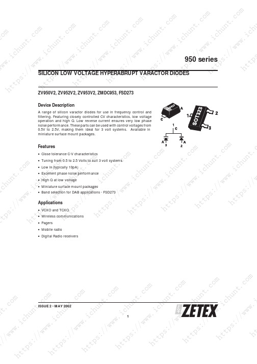
ZV950V2, ZV952V2, ZV953V2, ZMDC953, FSD273Device DescriptionA range of silicon varactor diodes for use in frequency control and filtering.Featuring closely controlled CV characteristics,low voltage operation and high Q.Low reverse current ensures very low phase noise performance.These parts can be used with control voltages from 0.5V to 2.5V,making them ideal for 3volt systems.Available in miniature surface mount packages.Features•Close tolerance C-V characteristics•Tuning from 0.5 to 2.5 Volts to suit 3 volt systems•Low I R (typically 10pA)•Excellent phase noise performance•High Q at low voltage•Miniature surface mount packages•Band selection for DAB applications - FSD273Applications•VCXO and TCXO•Wireless communications•Pagers •Mobile radio•Digital Radio receivers950 seriesISSUE 2 - MAY 20021SILICON LOW VOLTAGE HYPERABRUPT VARACTOR DIODESh tt ps ://w ww .i ch un t.co mh t t p sn t.co mh tt ps ://w ww .i ch un t.co mh tt p s://w w w.h tt ps ://w ww .i ch un t.co m.ic hu nt .c omh tt ps ://w ww .i ch un t.co mh tt p s://ww w.ih tt ps ://w ww .i ch un t.c o m w .i ch un t.co mt tp s://ww w.ic hu nt .c omh tt ps ://w ww .i ch tt ps ://w w w .i c h u n t .cww .i ch un t.co mi ch un t.co mh tt ps ://w ww .i ch h t t p s ://ww ww .i ch un t.co mh tt ps ://w ww .i ch u/w ww .i ch un t.co mh tt ps ://w ww .i ch un //w ww .i ch un t.co mh tt ps ://w ww .i ch un t://w ww .i c h u n t.c o mw ww .i ch un t.s ://w w w .i c950 seriesISSUE 2 - MAY 20022PARAMETER SYMBOL MAX UNIT Reverse voltageV R12V Forward currentI F100mAPower dissipation at T amb =25ЊC SOD523P tot250mW Power dissipation at T amb =25ЊC SOT323P tot300mWABSOLUTE MAXIMUM RATINGSPARAMETERCONDITIONS MIN.TYP.MAX.UNIT Reverse breakdown voltage I R =10uA 12V Reverse voltage leakageV R =8V0.01020nAELECTRICAL CHARACTERISTICS at Tamb = 25°CPART CAPACITANCE pF V R =0.5V,f=1MHzCAPACITANCE pFV R =1.5V,f=1MHzCAPACITANCE RATIO C 0.5/C 2.5f=1MHz Minimum Q V R =0.5V f=50MHzMinMin Max Min ZV950V29.5 6.37.8 2.0250ZV952V21912.715.7 2.0250ZV953V2453037 2.0200ZMDC953(DUAL)4530372.0250TUNING CHARACTERISTICS at T amb =25CZMDC953is available banded to tighter capacitance range.This product has the order code FSD273TA.Measured at VR=1.5V the bands are Band A = 30.0 to 32.5Band B = 32.3 to 34.7Band C = 34.5 to 37.0Product is supplied in reels.A banded reel will only contain a single band.Shipments containing several reels may have reels in different bands.It is not possible to supply a specific band as processing affects which bands are availableh tt ps ://w ww .i ch un t.co mh t t p sn t.co mh tt ps ://w ww .i ch un t.co mh tt p s ://w w w .h tt ps ://w ww .i ch un t.co m.ic hu nt .c omh tt ps ://w ww .i ch un t.co mh tt p s://ww w.ih tt ps ://w ww .i ch un t.co m w .i ch un t.co mt tp s://ww w.ic hu nt .c omh tt ps ://w ww .i ch tt ps ://w w w .i c h u n t .cww .i ch un t.co mi ch un t.co mh tt ps ://w ww .i ch h t t p s ://ww ww .i ch un t.co mh tt ps ://w ww .i ch u/w ww .i ch un t.co mh tt ps ://w ww .i ch un //w ww .i ch un t.co mh tt ps ://w ww .i ch un t://w ww .i c h u n t.c o m w ww .i ch un t.s ://w w w .i c950 seriesISSUE 2 - MAY 20023TYPICAL CHARACTERISTICSh tt p sn t .c o mh t t p s://w w w ..ic hu nt .c omh tt p s://ww w.iw .i ch un t.co t t p s ://tt ps ://w w w .i c ww .i ch un t.ci c h u n t .t ps ://w w w .i ch w ww .i ch un t.ps ://w ww .i ch u /w ww .i ch un ts ://w ww .i ch u n //w ww .i ch un h t t p ://w w w .i c h u n t://w ww .i ch uw w w .i ch u n t .s ://w ww .icORDER CODES AND PART MARKINGFSD273is a band selected version of the ZMDC953.Product is supplied in reels containing a single capacitance band.Shipments of several reels may contain reels of different bands.It is not possible for customers to specify a particular band,because availability is process depend-ent.950 seriesISSUE 2 - MAY 20024REEL CODEREEL SIZE TAPE WIDTHQUANTITY PER REELTA7inch (180mm)8mm3000TAPE AND REEL INFORMATIONh tt ps ://w ww .i ch uh t t p sn t.co mh tt ps ://w ww .i ch un h tt p s ://w w w .i c huh tt ps ://w ww .i ch .ic hu nt .c omh tt ps ://w ww .i ch un th tt p s://ww w.ic h u nt .c omh tt ps ://w ww .i ch un t .c o m w .i ch un t.co mt tp s://ww w.ic hu nt .c omh tt ps ://w ww .i ch un t.co mh tt ps ://w w w .i c h u n t .cww .i ch un t.co mi ch un t.co mh tt ps ://w ww .i ch un t.co mh t t p s ://ww ww .i ch un t.co mtt ps ://w ww .i ch un t.co m/w ww .i ch un t.co mh tt ps ://w ww .i ch un t.co m//w ww .i ch un t.co mh tt ps ://w ww .i ch un t.co m://w ww .i c h u n t.c o mw ww .i ch un t.co ms ://w w w .i c om950 seriesISSUE 2 - MAY 20025SOT323 PACKAGE DIMENSIONSMILLIMETRESMIN.MAX A ᎏ0.800A10.0000.100A20.6000.800b10.1600.300c 0.0800.220D 0.7000.900E 1.500 1.700E1 1.100 1.300L 0.2000.400L10.1700.230⍜1Њ4Њ10ЊSOD523 PACKAGE DIMENSIONSt t p s ://w w w .i c h u n o mh tt p s n t .c o mt p s ://w w w .i c h u n t h tt p s://w w w .i c huh t t p s ://w w w .i c h un t.c o m.ic hu nt .c omh t t p s ://w w w .i c h u n t .h t t p s ://w w w.ic hu nt .c omh t t p s ://w ww .i c h un t.co mw .i ch un t.co mt t p s ://w w w .i c h u n t .c t ps ://w w w .i c h un t.co mh tt ps ://w ww .i ch u n t.cww .i ch un t.co mi c h u n t .c o m ps ://w ww .i ch u n t.co mh t t p s ://ww ww .i ch un t.co s ://w ww .i ch un t.co m/w ww .i ch un t.ch tt ://w ww .i c h un t.co m//w ww .i ch un t.h t t p s ://w w w .i c h un t.c o m://w ww .i ch un t.co mw w w .i ch u n t .c o ms ://w ww .ic omZetex plcFields New Road ChaddertonOldham, OL9 8NP United KingdomTelephone (44) 161 622 4422Fax: (44) 161 622 4420Zetex GmbHStreitfeldstraße 19D-81673 München GermanyTelefon: (49) 89 45 49 49 0Fax: (49) 89 45 49 49 49Zetex Inc700 Veterans Memorial Hwy Hauppauge, NY11788USATelephone: (631) 360 2222Fax: (631) 360 8222Zetex (Asia) Ltd3701-04Metroplaza, Tower 1Hing Fong Road Kwai Fong Hong KongTelephone: (852) 26100 611Fax: (852) 24250 494These offices are supported by agents and distributors in major countries world-wide.This publication is issued to provide outline information only which (unless agreed by the Company in writing)may not be used,applied or reproduced for any purpose or form part of any order or contract or be regarded as a representation relating to the products or services concerned.The Company reserves the right to alter without notice the specification,design,price or conditions of supply of any product or service.For the latest product information,log on to© Zetex plc 2001950 series6ISSUE 2 - MAY 2002h tt ps ://w ww .i ch un t.co mh t t p sn t.co mh tt ps ://w ww .i ch un t.co mh tt p s ://w w w .i c huh tt ps ://w ww .i ch un t.co m.ic hu nt .c omh tt ps ://w ww .i ch un t.co mh tt p s://ww w.ic h u nt .c omh tt ps ://w ww .i ch un t .c o m w .i ch un t.co mt tp s://ww w.ic hu nt .c omh tt ps ://w ww .i ch un t.co mh tt ps ://w w w .i c h u n t .cww .i ch un t.co mi ch un t.co mh tt ps ://w ww .i ch un t.co mh t t p s ://ww ww .i ch un t.co mh tt ps ://w ww .i ch un t.co m/w ww .i ch un t.co mh tt ps ://w ww .i ch un t.co m//w ww .i ch un t.co mh tt ps ://w ww .i ch un t.co m://w ww .i c h u n t.c o mw ww .i ch un t.co ms ://w w w .i c om。

SUMMARY PNP Transistor V CEO =-12V;R SAT = 65m ;C = -4A Schottky Diode V R = 40V; V F = 500mV (@1A); I C =1ADESCRIPTIONPackaged in the new innovative 3mm x 2mm MLP this combination dual comprises an ultra low saturation PNP transistor and a 1A Schottky barrier diode.This excellent combination provides users with highly efficient performance in applications including DC-DC and charging ers will also gain several other key benefits :Performance capability equivalent to much larger packages Improved circuit efficiency & power levelsPCB area and device placement savingsLower package height (0.9mm nom)Reduced component countFEATURES•Extremely Low Saturation Voltage (-140mV @1A)•H FE characterised up to -10A•I C = -4A Continuous Collector Current•Extremely Low V F , fast switching Schottky•3mm x 2mm MLPAPPLICATIONS•DC - DC Converters •Mobile Phones•Charging Circuits •Motor controlDEVICE MARKING1S1ZX3CD1S1M832ISSUE 1 - JUNE 2002MPPS™ Miniature Package Power Solutions12V PNP LOW SATURATION TRANSISTOR AND 40V, 1A SCHOTTKY DIODE COMBINATION DUAL1DEVICEREEL TAPE WIDTH QUANTITY PER REELZX3CD1S1M832TA 78mm 3000ZX3CD1S1M832TC138mm10000ORDERING INFORMATION3mm x 2mm Dual DieMLP3mm x 2mm Dual MLPunderside viewPINOUTh tt ps ://w ww .i ch un o mh t t p sn t.co mh tt ps ://w ww .i ch un t.co mh tt p s://w w w.h tt ps :co m.ic hu nt .c omh tt ps ://w ww .i ch un t.co mh tt p s://ww w.ih tt n t.c o m w .i ch un t.co mt tp s://ww w.ic hu nt .c omh tt ps ://w ww .i ch tt ://w w w .i c h u n t .cww .i ch un t.co mi ch un t.co mh tt ps ://w ww .i ch h t t p s ://ww ww .i ch un t.co mh tt ps ://w ww .i ch u/w ww .i ch un t.co mh tt ps ://w ww .i ch un //w ww .i ch un t.co mh tt ps ://w ww .i ch un t://w ww .i c h u n t.c o mw ww .i ch un t.s ://w w w .i cZX3CD1S1M832ISSUE 1 - JUNE 20022PARAMETERSYMBOL VALUE UNIT TransistorCollector-Base VoltageV CBO -20V Collector-Emitter Voltage V CEO -12V Emitter-Base Voltage V EBO -7.5V Peak Pulse CurrentI CM -12A Continuous Collector Current (a)(f)I C -4A Continuous Collector Current (b)(f)I C -4.4A Base CurrentI B 1000mA Power Dissipation at TA=25°C (a)(f)Linear Derating FactorP D 1.512W mW/°C Power Dissipation at TA=25°C (b)(f)Linear Derating FactorP D 2.4519.6W mW/°CPower Dissipation at TA=25°C (c)(f)Linear Derating FactorP D18W mW/°CPower Dissipation at TA=25°C (d)(f)Linear Derating FactorP D 1.139W mW/°CPower Dissipation at TA=25°C (d)(g)Linear Derating Factor P D1.713.6W mW/°CPower Dissipation at TA=25°C (e)(g)Linear Derating FactorP D324W mW/°CStorage Temperature RangeT stg-55to +150°C Junction TemperatureT j150°CABSOLUTE MAXIMUM RATINGS.PARAMETER SYMBOL VALUE UNIT Junction to Ambient (a)(f)R θJA 83°C/W Junction to Ambient (b)(f)R θJA 51°C/W Junction to Ambient (c)(f)R θJA 125°C/W Junction to Ambient (d)(f)R θJA 111°C/W Junction to Ambient (d)(g)R θJA 73.5°C/W Junction to Ambient (e)(g)R θJA41.7°C/WTHERMAL RESISTANCENotes(a) For a dual device surface mounted on 8 sq cm single sided 2oz copper on FR4 PCB, in still air conditions with all exposed pads attached . The copper area is split down the centre line into two separate areas with one half connected to each half of the dual device.(b) Measured at t<5 secs for a dual device surface mounted on 8 sq cm single sided 2oz copper on FR4 PCB, in still air conditions with all exposed pads attached.The copper area is split down the centre line into two separate areas with one half connected to each half of the dual device.(c) For a dual device surface mounted on 8 sq cm single sided 2oz copper on FR4 PCB, in still air conditions with minimal lead connections only.(d) For a dual device surface mounted on 10 sq cm single sided 1oz copper on FR4 PCB, in still air conditions with all exposed pads attached attached . The copper area is split down the centre line into two separate areas with one half connected to each half of the dual device.(e) For a dual device surface mounted on 85 sq cm single sided 2oz copper on FR4 PCB, in still air conditions with all exposed pads attached attached . The copper area is split down the centre line into two separate areas with one half connected to each half of the dual device.(f) For a dual device with one active die.(g) For dual device with 2 active die running at equal power.(h) Repetitive rating - pulse width limited by max junction temperature. Refer to Transient Thermal Impedance graph.(i) The minimum copper dimensions required for mounting are no smaller than the exposed metal pads on the base of the device as shown in the package dimensions data. The thermal resistance for a dual device mounted on 1.5mm thick FR4 board using minimum copper 1 oz weight, 1mm wide tracks and one half of the device active is Rth = 250°C/W giving a power rating of Ptot = 500mW.h tt ps ://w ww .i ch un t.co mh t t p sn t.co mh tt ps ://w ww .i ch un t.co mh tt p s ://ww w .h tt ps ://w ww .i ch un t.co m.ic hu nt .c omh tt ps ://w ww .i ch un t.co mh tt p s://ww w.ih tt ps ://w ww .i ch un t .c o m w .i ch un t.co mt tp s://ww w.ic hu nt .c omh tt ps ://w ww .i ch tt ps ://w w w .i c h un t .cww .i ch un t.co mi ch un t.co mh tt ps ://w ww .i ch h t t p s ://ww ww .i ch un t.co mh tt ps ://w ww .i ch u/w ww .i ch un t.co mh tt ps ://w ww .i ch un //w ww .i ch un t.co m h tt ps ://w ww .i ch un t://w ww .i ch u n t.c o m w ww .i ch un t.s ://w w w .i cZX3CD1S1M832ISSUE 1 - JUNE 20023TRANSISTOR TYPICAL CHARACTERISTICSh t t p sn t.co mh tt p s://w w w ..ic hu nt .c omh tt p s://ww w.io m w .i ch un t.co tt ps ://w ww .i cw w .i c h u n t .c ww .i ch un t.ct ps ://w ww .i ch h t t p s ://ww ww .i ch un t.ps ://w ww .i ch u/w ww .i ch un ts ://w ww .i ch un //w ww .i ch un ://w ww .i ch un t://w ww .i c h u n t.c o m w ww .i ch un t.s ://w w w .icZX3CD1S1M832ISSUE 1 - JUNE 20024PARAMETERSYMBOL VALUE UNIT Schottky DiodeContinuous Reverse VoltageV R 40V Forward Voltage @I F =1000mA(typ)V F 425A Forward CurrentI F 1850mA Average Peak Forward Current D=50%I FAV 3A Non Repetitive Forward Current t ≤100st ≤10ms I FSM 127A A Power Dissipation at TA=25°C (a)(f)Linear Derating FactorP D 1.212W mW/°C Power Dissipation at TA=25°C (b)(f)Linear Derating FactorP D 220W mW/°C Power Dissipation at TA=25°C (c)(f)Linear Derating FactorP D0.88W mW/°C Power Dissipation at TA=25°C (d)(f)Linear Derating FactorP D0.99W mW/°C Power Dissipation at TA=25°C (d)(g)Linear Derating FactorP D 1.3613.6W mW/°CPower Dissipation at TA=25°C (e)(g)Linear Derating Factor P D2.424W mW/°C Storage Temperature RangeT stg-55to +150°CJunction TemperatureT j125°CABSOLUTE MAXIMUM RATINGS.PARAMETER SYMBOL VALUE UNIT Junction to Ambient (a)(f)R θJA83°C/W Junction to Ambient (b)(f)R θJA 51°C/W Junction to Ambient (c)(f)R θJA 125°C/W Junction to Ambient (d)(f)R θJA 111°C/W Junction to Ambient (d)(g)R θJA 73.5°C/W Junction to Ambient (e)(g)R θJA41.7°C/WTHERMAL RESISTANCENotes(a) For a dual device surface mounted on 8 sq cm single sided 2oz copper on FR4 PCB, in still air conditions with all exposed pads attached . The copper area is split down the centre line into two separate areas with one half connected to each half of the dual device.(b) Measured at t<5 secs for a dual device surface mounted on 8 sq cm single sided 2oz copper on FR4 PCB, in still air conditions with all exposed pads attached.The copper area is split down the centre line into two separate areas with one half connected to each half of the dual device.(c) For a dual device surface mounted on 8 sq cm single sided 2oz copper on FR4 PCB, in still air conditions with minimal lead connections only.(d) For a dual device surface mounted on 10 sq cm single sided 1oz copper on FR4 PCB, in still air conditions with all exposed pads attached attached . The copper area is split down the centre line into two separate areas with one half connected to each half of the dual device.(e) For a dual device surface mounted on 85 sq cm single sided 2oz copper on FR4 PCB, in still air conditions with all exposed pads attached attached . The copper area is split down the centre line into two separate areas with one half connected to each half of the dual device.(f) For a dual device with one active die.(g) For dual device with 2 active die running at equal power.(h) Repetitive rating - pulse width limited by max junction temperature. Refer to Transient Thermal Impedance graph.(i) The minimum copper dimensions required for mounting are no smaller than the exposed metal pads on the base of the device as shown in the package dimensions data. The thermal resistance for a dual device mounted on 1.5mm thick FR4 board using minimum copper 1 oz weight, 1mm wide tracks and one half of the device active is Rth = 250°C/W giving a power rating of Ptot = 400mW.h tt ps ://w ww .i ch un t.co mh t t p sn t.co mh tt ps ://w ww .i ch un t.co mh tt p s ://ww w .h tt ps ://w ww .i ch un t.co m.ic hu nt .c omh tt ps ://w ww .i ch un t.co mh tt p s://ww w.ih tt ps ://w ww .i ch un t .c o m w .i ch un t.co mt tp s://ww w.ic hu nt .c omh tt ps ://w ww .i ch tt ps ://w w w .i c h un t .cww .i ch un t.co mi ch un t.co mh tt ps ://w ww .i ch h t t p s ://ww ww .i ch un t.co mh tt ps ://w ww .i ch u/w ww .i ch un t.co mh tt ps ://w ww .i ch un //w ww .i ch un t.co m h tt ps ://w ww .i ch un t://w ww .i c h u n t.c o m w ww .i ch un t.s ://w w w .i cZX3CD1S1M832ISSUE 1 - JUNE 20025SCHOTTKY TYPICAL CHARACTERISTICSh t t p sn t.co mh tt p s://w w w ..ic hu nt .c omh tt p s://ww w.io m w .i ch un t.co mt tp stt ps ://w ww .i cw w .i c h u n t .c ww .i ch un t.co mi ch ut ps ://w ww .i ch h t t p s ://ww ww .i ch un t.co mps ://w ww .i ch u/w ww .i ch un t.co ms ://w ww .i ch un //w ww .i ch un t.co m h ://w ww .i ch un t://w ww .i c h u n t.c o m w ww .i ch un t.s ://w w w .icZX3CD1S1M832ISSUE 1 - JUNE 20026PARAMETERSYMBOLMIN.TYP.MAX.UNITCONDITIONS.TRANSISTOR ELECTRICAL CHARACTERISTICS Collector-Base Breakdown VoltageV (BR)CBO -20-35V I C =-100A Collector-Emitter Breakdown VoltageV (BR)CEO -12-25V I C =-10mA*Emitter-Base Breakdown Voltage V (BR)EBO -7.5-8.5V I E =-100A Collector Cut-Off Current I CBO -25nA V CB =-16V Emitter Cut-Off CurrentI EBO -25nA V EB =-6V Collector Emitter Cut-Off Current I CES -25nA V CES =-10VCollector-Emitter Saturation VoltageV CE(sat)-10-100-100-195-240-17-140-150-300-300mV mV mV mV mV I C =-0.1A,I B =-10mA*I C =-1A,I B =-10mA*I C =-1.5A,I B =-50mA*I C =-3A,I B =-50mA*I C =-4A,I B =-150mA*Base-Emitter Saturation VoltageV BE(sat)-0.97-1.05V I C =-4A,I B =-150mA*Base-Emitter Turn-On VoltageV BE(on)-0.87-0.950VI C =-4A,V CE =-2V*Static Forward Current Transfer Ratioh FE300300180604547545027510070I C =-10mA,V CE =-2V*I C =-0.1A,V CE =-2V*I C =-2.5A,V CE =-2V*I C =-8A,V CE =-2V*I C =-10A,V CE =-2V*Transition Frequencyf T100110MHzI C =-50mA,V CE =-10V f=100MHzOutput Capacitance C obo2130pFV CB =-10V,f=1MHzTurn-On Timet (on)70nsV CC =-6V,I C =-2A I B1=I B2=-50mATurn-Off Timet (off)130nsSCHOTTKY DIODE ELECTRICAL CHARACTERISTICSReverse Breakdown VoltageV (BR)R4060V I R =300AForward VoltageV F240265305355390425495420270290340400450500600—mV mV mV mV mV mV mV mV I F =50mA*I F =100mA*I F =250mA*I F =500mA*I F =750mA*I F =1000mA*I F =1500mA*I F =1000mA,T a =100°C*Reverse Current I R 50100A V R =30VDiode Capacitance C D 25pF f=1MHz,V R =25V Reverse Recovery Timet rr12nsswitched fromI F =500mA to I R =500mA Measured at I R = 50mAELECTRICAL CHARACTERISTICS (at T amb = 25°C unless otherwise stated).*Measured under pulsed conditions.h tt ps ://w ww .i ch un t.co mh t t p sn t.co mh tt ps ://w ww .i ch un t.co mh tt p s ://ww w .h tt ps ://w ww .i ch un t.co m.ic hu nt .c omh tt ps ://w ww .i ch un t.co mh tt p s://ww w.ih tt ps ://w ww .i ch un t .c o m w .i ch un t.co mt tp s://ww w.ic hu nt .c omh tt ps ://w ww .i ch tt ps ://w w w .i c h un t .cww .i ch un t.co mi ch un t.co mh tt ps ://w ww .i ch h t t p s ://ww ww .i ch un t.co mh tt ps ://w ww .i ch u/w ww .i ch un t.co mh tt ps ://w ww .i ch un //w ww .i ch un t.co m h tt ps ://w ww .i ch un t://w ww .i c h u n t.c o m w ww .i ch un t.s ://w w w .i cISSUE 1 - JUNE 20027h t t p sn t .c o m://w w w..ic hu nt .c omh t w.io m w .i ch un t.co t t p s ://w w w .i .i cw w .i c h u n t .c ww .i ch un t.ci c h u n t .c o m i ch h t t p s ://ww ww .i ch un t.ch u/w ww .i ch un th un //w ww .i ch un h t t p s ://w un t://w ww .i ch un t.co mw w w .i ch u n t .s ://w ww .icZX3CD1S1M832ISSUE 1 - JUNE 20028SCHOTTKY TYPICAL CHARACTERISTICSh tt p sn t.co mh tt p s://ww w..ic hu nt .c h th t t p s://ww w.imw .i ch un t.t t p s ://w w w .i tt ps ://w ww .i cw .i c h un t.cww .i ch un ti c h u n t .c o m t p s ://w ww .i ch h t t p s ://ww ww .i ch un ps ://w w w .i ch u/w ww .i ch us ://w ww .i ch un //w ww .i ch h t t p s ://w w w .i c h un t://w ww .i ch un t.co mw w w .i ch un t.s ://w ww .icZX3CD1S1M832ISSUE 1 - JUNE 20029EuropeZetex plcFields New Road ChaddertonOldham, OL9 8NP United KingdomTelephone (44) 161 622 4422Fax: (44) 161 622 4420uksales@Zetex GmbHStreitfeldstraße 19D-81673 München GermanyTelefon: (49) 89 45 49 49 0Fax: (49) 89 45 49 49 49europe.sales@AmericasZetex Inc700 Veterans Memorial Hwy Hauppauge, NY11788USATelephone: (631) 360 2222Fax: (631) 360 8222usa.sales@Asia PacificZetex (Asia) Ltd3701-04Metroplaza, Tower 1Hing Fong Road Kwai Fong Hong KongTelephone: (852) 26100 611Fax: (852) 24250 494asia.sales@These offices are supported by agents and distributors in major countries world-wide.This publication is issued to provide outline information only which (unless agreed by the Company in writing)may not be used,applied or reproduced for any purpose or form part of any order or contract or be regarded as a representation relating to the products or services concerned.The Company reserves the right to alter without notice the specification,design,price or conditions of supply of any product or service.For the latest product information,log on to©Zetexplc 2002CONTROLLING DIMENSIONS IN MILLIMETRES APPROX. CONVERTED DIMENSIONS IN INCHESDIM MILLIMETRESINCHES DIM MILLIMETRES INCHES MIN.MAX.MIN.MAX.MIN.MAX.MIN.MAX.A 0.80 1.000.0310.039e 0.65REF 0.0256BSC A10.000.050.000.002E 2.00BSC 0.0787BSC A20.650.750.02550.0295E20.430.630.0170.0249A30.150.250.0060.0098E40.160.360.0060.014b 0.240.340.0090.013L 0.200.450.00780.0157b10.170.300.00660.0118L20.1250.000.005D 3.00BSC 0.118BSC r 0.075BSC0.0029BSCD20.82 1.020.0320.040⍜0Њ12Њ0Њ12ЊD31.011.210.03970.0476MLP832 PACKAGE DIMENSIONS。
SCHEMATIC DIAGRAMPRECISION 1.25 VOLTMICROPOWER VOLTAGE REFERENCEISSUE 2 - MARCH 1998VRG ndDEVICE DESCRIPTIONThe ZREF12 uses a bandgap circuit design to achieve a precision micropower voltage reference of 1.24 volts. The device is available in a small outline surface mount package, ideal for applications where space saving is important, as well as packages for through hole requirements.The ZREF12 design provides a stable voltage without an external capacitor and is stable with capacitive loads. The ZREF12 is recommended for operation between 50µA and 5mA and so is ideally suited to low power and battery powered applications.Excellent performance is maintained to an absolute maximum of 25mA, however the rugged design and 20 volt processing allows the reference to withstand transient effects and currents up to 200mA. Superior switching capability allows the device to reach stable operating conditions in only a few microseconds.FEATURES•Small outline SO8 and TO92 stylepackages•No stabilising capacitor required •Typical T C 30ppm/°C•Typical slope resistance 0.65Ω•± 1% tolerance•Industrial temperature range (Military temperature range available on request)•Operating current 50µA to 5mA•T ransient response, stable in less than 10µs•Alternative package options and tolerances availableAPPLICATIONS•Battery powered and portable equipment.•Metering and measurement systems.•Instrumentation.•Precision power supplies.•Test equipment.•Data acquisition systemshttps://https:// https://https:// httpshttps://https:// https://wwwhttps://:// https://www.ichunhttps://www.ichun://https://https://wwwhttps://https://httpshttps://https://ABSOLUTE MAXIMUM RATINGReverse Current 25mAForward Current25mAOperating Temperature -40 to 85°C Storage Temperature-55 to 125°CPower Dissipation (Tamb =25°C)E-Line, 3 pin (TO92)500mW E-Line, 2 pin (TO92)500mW SO8625mWELECTRICAL CHARACTERISTICSTEST CONDITIONS (Unless otherwise stated) T amb=25°Chttps://httpshttps://www:// https://www.ichunhttps://www.ichunhttps://https://wwwhttps://httpsTYPICAL CHARACTERISTICShttpshttps://https://www:// https://www.ichunhttps://www.ichunhttps://https://wwwhttps://httpsCONNECTION DIAGRAMS* E-Line 3 pin Reversed † E-Line 2 pinORDERING INFORMATION httpshttps://https://wwwhttps://:// https://www.ichunhttps://www.ichunhttps://https://wwwhttps://httpshttps://https://。
S E M I C O N D U C T O R SDESCRIPTIONThe ZMZ20is an extremely sensitive magnetic field sensor in a 4pin E-Line package employing the magneto-resistive effects of thin film Permalloy.It allows the measurement of magnetic fields or the detection of metallic parts.The sensor consists of a chip covered with Permalloy stripes which form a Wheatstone bridge,whose output voltage is proportional to the magnetic field component Hy.A perpendicular field Hx is necessary to suppress the hysteresis and this can be provided by using a small permanent magnet.FEATURES•Output voltage proportional to magnetic field Hy•Adjustment of sensitivity and suppression ofhysteresis by the auxiliary magnetic field Hx •Magnetic fields vertical to the chip level are noteffectiveAPPLICATIONS•Linear position sensors for process control,door interlocks,proximity detectors,machine tool sensing•Scalar measurement for compassing•Automotive - door switches, engine position andspeed sensing•Metering of fluids by sensing rotation of impeller •Traffic counting and vehicle-type sensing •Measurement of current in a conductor withoutconnectionDEVICE MARKING•M20ZMZ20ISSUE 2 - JANUARY 2004MAGNETIC FIELD SENSORS1E-LINEPINOUTSIDE VIEWDEVICE BOXZMZ20Bulk in box (2,000components per box)ORDERING INFORMATIONhttps://https://https://https://httpshttps://https://:// https://www.ichun://https://https:// https://httpshttps://ZMZ20S E M I C O N D U C T O R SISSUE 2 - JANUARY 2004 2PARAMETER SYMBOL LIMIT UNIT Supply voltage V B12VTotal power dissipation P TOT120mW Operating temperature range T amb-40 to +150°C ABSOLUTE MAXIMUM RATINGSPARAMETER SYMBO MIN.TYP.MAX.UNIT CONDITIONSBridge resistance R br 1.2 1.7 2.2k⍀Output voltage range V O/V B162024mV/VOpen circuit sensitivity S 3.7 4.7 5.7(mV/V)/(kA/m)No disturbing field H dallowedHysteresis of output voltage V OH/V B--50µV/V Hy=2kA/mOffset voltage V off/V B-1.0-+1.0mV/VOperating frequency f max0-1MHzTemperature coefficient of offset voltages TCV off-3-+3(µV/V)/K T amb=-25to+125°CTemperature coefficient of bridgeresistanceTCR br0.250.30.35%/K T amb=-25to+125°CTemperature coefficient of opencircuit sensitivityV B=5VTCS V-0.25-0.3-0.35%/K T amb=-25to+125°CTemperature coefficient of open circuit sensitivityI B=3mA TCS I--0.1-%/K T amb=-25to+125°CELECTRICAL CHARACTERISTICS(at T amb= 25°C and Hx=3kA/m unless otherwise stated)https://https://https://https:// httpshttps://https:// https://wwwhttps:// :// https://www.ichunhttps://www.ichun :// https://https://www https:// https://https https://ZMZ20S E M I C O N D U C T O R SISSUE 2 - JANUARY 20043Application 2 (analog output)Application 1 (digital output)httpshttps://https://httpshttps://ZMZ20S E M I C O N D U C T O R S ISSUE 2 - JANUARY 20044https https:// https://https https://ZMZ20S E M I C O N D U C T O R SISSUE 2 - JANUARY 20045httpshttps://https://httpshttps://。
AD4000/AD4004/AD4008Data Sheet Rev. E | Page 2 of 40TABLE OF CONTENTSFeatures (1)Applications (1)Functional Block Diagram (1)General Description (1)Revision History (2)Specifications (5)Timing Specifications (8)Absolute Maximum Ratings (10)Thermal Resistance (10)ESD Caution (10)Pin Configurations and Function Descriptions (11)Typical Performance Characteristics (12)Terminology (18)Theory of Operation (19)Circuit Information (19)Converter Operation (20)Transfer Functions (20)Applications Information (21)Typical Application Diagrams (21)Analog Inputs .............................................................................. 22 Driver Amplifier Choice ........................................................... 23 Ease of Drive Features ............................................................... 24 Voltage Reference Input ............................................................ 25 Power Supply ............................................................................... 25 Digital Interface .......................................................................... 25 Register Read/Write Functionality........................................... 28 Status Bits .................................................................................... 30 CS Mode, 3-Wire Turbo Mode ................................................. 31 CS Mode, 3-Wire Without Busy Indicator ............................. 32 CS Mode, 3-Wire with Busy Indicator .................................... 33 CS Mode, 4-Wire Turbo Mode ................................................. 34 CS Mode, 4-Wire Without Busy Indicator ............................. 35 CS Mode, 4-Wire with Busy Indicator .................................... 36 Daisy-Chain Mode ..................................................................... 37 Layout Guidelines....................................................................... 38 Evaluating the AD4000/AD4004/AD4008 Performance ...... 38 Outline Dimensions ....................................................................... 39 Ordering Guide .......................................................................... 40 REVISION HISTORY2/2021—Rev. D to Rev. EChanges to Features Section, Applications Section, GeneralDescription Section (1)Changes to Specifications Section and Table 1 (5)Changes to Timing Specifications Section (8)Added Note 1 to Table 2; Renumbered Sequentially ................... 8 Deleted Timing Diagram Section and Figure 3; RenumberedSequentially (8)Added Note 1 to Table 3; Renumbered Sequentially (9)Changes to Thermal Resistance Section (10)Changes to Table 7 (11)Changes to Effective Number of Bits (ENOB) Section (18)Changes to Figure 7 Caption and Figure 10 Caption (12)Changes to Figure 11 and Figure 14 (12)Changes to Circuit Information Section and Table 8 (19)Changes to Typical Application Diagrams Section .................... 21 Changes to Input Overvoltage Clamp Circuit Section .............. 22 Changes to Table 10, Driver Amplifier Choice Section, andHigh Frequency Input Signals Section ........................................ 23 Changes to Multiplexed Applications Section, Input SpanCompression Section, and High-Z Mode Section ..................... 24 Changes to Figure 44 Caption, Figure 45 Caption, Voltage Reference Input Section, and Digital Interface Section ............ 25 Changes to Register Read/Write Functionality Section and Figure 46 .......................................................................................... 28 Changes to Figure 47 ...................................................................... 29 Changes to Status Bit Section and Figure 49 .............................. 30 Changes to CS Mode, 3-Wire Turbo Mode Section .................. 31 Changes to CS Mode, 3-Wire Without Busy Indicator Section ...... 32 Changes to CS Mode, 3-Wire With Busy Indicator Section, Figure 54, and Figure 55 ................................................................ 33 Changes to CS Mode, 4-Wire Turbo Mode Section .................. 34 Changes to CS Mode, 4-Wire Without Busy Indicator Section ...... 35 Changes to CS Mode, 4-Wire with Busy Indicator Section and Figure 61 .......................................................................................... 36 Changes to Daisy-Chain Mode Section and Figure 62 ............. 37 Changes to Layout Guidelines and Evaluating the AD4000/AD4004/AD4008 Performance Section ............................. 38 Updated Outline Dimensions................................................................ 39 Changes to Ordering Guide . (40)Data SheetAD4000/AD4004/AD4008Rev. E | Page 3 of 408/2019—Rev. C to Rev. DAdded Figure 2; Renumbered Sequentially (1)Changes to Features Section and General Description Section (1)Added Figure 18 and Figure 21 (13)Added Figure 27, Figure 28, and Figure 29 (14)Added Figure 33 and Figure 35 (15)Changes to Figure 31 and Figure 32 (15)Changes to Figure 38 (18)Changes to Input Overvoltage Clamp Circuit Section (21)Changes to High-Z Mode Section, Figure 45, and Figure 46 .... 23 Added Configuration Register Details Section and Serial ClockFrequency Requirements Section (24)Changes to Digital Interface Section (24)Deleted Table 12 and Table 13; Renumbered Sequentially (25)Added Table 12 and Table 13; Renumbered Sequentially .......... 25 Changes to Register Read/Write Functionality Section andFigure 47 (26)Changes to Figure 48 (27)Added Table 58 ................................................................................ 28 Changes to Status Bits Section ....................................................... 28 Changes to CS Mode, 3-Wire Turbo Mode Section andFigure 51 ........................................................................................... 29 Changes to CS Mode, 3-Wire Without Busy Indicator Sectionand Figure 53 ................................................................................... 30 Changes to CS Mode, 3-Wire with Busy Indicator Section andFigure 55 ........................................................................................... 31 Changes to CS Mode, 4-Wire Turbo Mode Section andFigure 57 ........................................................................................... 32 Changes to CS Mode, 4-Wire Without Busy Indicator Sectionand Figure 59 ................................................................................... 33 Changes to CS Mode, 4-Wire with Busy Indicator Section andFigure 61 (34)Changes to Daisy-Chain Mode Section and Figure 64 (35)Updated Outline Dimensions (37)Changes to Ordering Guide ........................................................... 38 10/2017—Rev. B to Rev. CChanges to Features Section (1)Added Multiplexed Applications Section (21)Changes to Ordering Guide (36)Added Timing Diagram Section (8)Moved Figure 3 .................................................................................. 8 9/2017—Rev. A to Rev. BAdded AD4008 ................................................................... Universal Changes to Title, Features Section, General Description Section,and Figure 1 (1)Changes to Table 1 (4)Changes to Timing Specifications Section and Table 2 (7)Changes to Table 4 (8)Changes to Table 5 ............................................................................ 9 Changes to Typical Performance Characteristics Section Layout .. 11 Changes to Figure 19 ............................................................................... 13 Added Figure 25; Renumbered Sequentially ............................... 14 Changes to Figure 28 ...................................................................... 14 Change to Zero Error Definition, Terminology Section ........... 16 Changes to Circuit Information Section and Table 8 ................. 17 Changes to Converter Operation Section and Note 1 and Note 2, Table 9 ................................................................................. 18 Changes to High Frequency Input Signals Section, Figure 36 Caption, and Figure 37 Caption .................................................... 21 Added Figure 38 .............................................................................. 21 Changes to Input Span Compression Section, High-Z Mode Section, Figure 40, and Figure 41 Caption................................... 22 Changes to Figure 42 Caption, Figure 43 Caption, Power Supply Section, and Figure 44 Caption ..................................................... 23 Changes to Figure 45, Digital Interface Section, and Table 11 ........ 24 Changes to Register Read/Write Functionality Section and Figure 46 Caption ............................................................................ 25 Changes to CS Mode, 3-Wire Turbo Mode Section ................... 28 Changes to CS Mode, 3-Wire with Busy Indicator Section ...... 30 Changes to CS Mode, 4-Wire Turbo Mode Section ................... 31 Changes to CS Mode, 4-Wire with Busy Indicator Section ...... 33 Changes to Daisy-Chain Mode Section ....................................... 34 Changed Evaluating the AD4000/AD4004 Performance Section to Evaluating the AD4000/AD4004/AD4008 Performance Section .............................................................................................. 35 Changes to Evaluating the AD4000/AD4004/AD4008 Performance Section ....................................................................... 35 Changes to Ordering Guide ........................................................... 36 4/2017—Rev. 0 to Rev. A Added AD4004 ................................................................... Universal Changes to Title, Features Section, General Description Section, and Figure 1 ....................................................................................... 1 Changes to Table 1 ............................................................................ 3 Changes to Table 2 ............................................................................ 6 Changes to Table 4 ............................................................................ 7 Changes to Table 7 ............................................................................ 9 Changes to Figure 19 and Figure 21 ............................................. 12 Changes to Figure 24 ...................................................................... 13 Added Figure 25; Renumbered Sequentially ............................... 13 Moved Terminology Section ......................................................... 15 Changes to Circuit Information Section and Table 8 ................. 16 Changes to Figure 33 ...................................................................... 18 Changes to RC Filters Section ....................................................... 19 Changes to High Frequency Input Signals Section .................... 20 Changes to High-Z Mode Section, Figure 38, and Figure 39 .... 21 Changes to Long Acquisition Phase Section and Figure 43 ...... 22 Changes to Digital Interface Section and Register Read/Write Functionality Section . (23)Changes to Figure 45 (24)。
ZMR seriesFixed 2.5, 3.3 and 5 volt miniature voltage regulatorsDescriptionOrdering informationThe ZMR series of three terminal fixed positive voltage regulators feature internal current limit and will shut down under thermal overload conditions making the devices difficult to destroy.The circuit design offers an exceptionally low quiescent current, only 30µA for the 2.5V device, ideal for low power applications. The initial devices in the series regulate to 2.5 or 5V with a drive capability up to 50mA.The device is designed with space saving in mind and is available in the small outline SOT23package. The ZMR250 has expanded its input voltage range to 22.5V and the ZMR500 has expanded its input voltage range to 25V;equalling that of the ZMR25H and ZMR50H respectively.The ZMR330 provides a 3.3V output over an input range of 5V to 24V.Features•Small outline SOT23 package • 2.5V, 3.3V and 5V output•Output current up to 50mA •Very low quiesent current (30µA)•Unconditionally stable•Internal short circuit current limitPinout detailsOrder reference Package Part mark Status Reel size (inches)Quantity per reel Tape width (mm)Price ($) 1kZMR25HCL TO92ZMR25H Obsolete Loose 4000--ZMR25HCSTZ TO92ZMR25H Obsolete -1500-ZMR25HFTA SOT2325X LTB 30/06/20077"30008mm0.551ZMR250CL TO92ZMR250Obsolete Loose 4000-ZMR250CSTOB TO92ZMR250Obsolete 12.5"1500--ZMR250CSTZ TO92ZMR250Obsolete -1500--ZMR250FTA SOT2325K Active 7"30008mm 0.382ZMR330FTA SOT23330Active 7"30008mm 0.382ZMR50HCL TO92ZMR50H Obsolete Loose 4000-ZMR50HCSTZ TO92ZMR50H Obsolete -1500-ZMR50HFTA SOT2350R LTB 30/06/20077"30008mm 0.551ZMR500CL TO92ZMR500LTB 31/05/2007Loose 4000-0.486ZMR500CSTZ TO92ZMR500LTB 31/05/2007Concertina1500-0.486ZMR500FTA SOT2350K Active 7"30008mm 0.424ZMR500FTCSOT2350KLTB 30/06/200713"100008mm 0.424https://httpshttps:// https://https://wwwhttps:// :// https://www.ichunhttps://www.ichun:// https://https://wwwhttps://https:// httpshttps://Absolute maximum ratingsNote:1. The maximum operating input voltage and output current of the device will be governed bythemaximum power dissipation of the selected package. Maximum package power dissipationis specified at 25°C and must be linearly derated to zero at T amb =125°C.2. The following data represents pulse test conditions with junction temperatures as indicated atthe initiation of the test. Continuous operation of the devices with the stated conditionsmightexceed the power dissipation limits of the chosen package.3. Maximum power dissipation for the SOT23 package, is calculated assuming that the device ismounted on a ceramic substrate measuring 15 x 15 x 0.6mm.Input voltage (ZMR25H)22.5V ZMR25020V (ZMR50H)25VZMR50020VPackage power dissipation SOT23 500mW (Note 3)(T amb =25 °C)TO92 600mW Output current (I O )100mA Operating temperature -55 to 125°C Storage temperature-65 to 150°Chttps://https://https://https://httpshttps://https:// https://www https://:// https://www.ichunhttps://www.ichun:// https://https://wwwhttps:// https://httpshttps://ZMR25H and ZMR250Electrical characteristics test conditions (unless otherwise stated):T j =25°C,I O = 10mA, V IN = 6.5VSymbol Parameter ConditionsMin.Typ. Max. UnitsV OOutput voltage2.438 2.5 2.563 V I O =0 to 50mAT j =-55 to 125°C 2.360 2.640 V V IN =4.5 to 22.5V2.3602.640VI O =0 to 50mA T j =-55 to 125°C⌬V O Lineregulation V IN =4.5 to 22.5V5 15 mV ⌬VOLoad regulation I O=0 to 50mA 20 30mV I O =0 to 10mA12 mV l S Supply currentT j=-55 to 125°C 30 40 µA ⌬l SSupply current changeI O =0 to 50mA 1 ±10 µA V IN =4.5 to 22.5V210 µA V NOutput noise voltagef=10Hz to 10kHz 65µV rms ⌬V IN /⌬V O Ripplerejection V IN =6.3 to 18Vf=120Hz55 75dB V INInput voltage required tomaintain regulation4.2 3.9V⌬V O /⌬T Average temperaturecoefficient of V OI O =5.0mAT j =-55 to 125°C0.275 0.700 mV/°Chttps:// https://https:// https:// httpshttps://https://https://wwwhttps:// :// https://www.ichunhttps://www.ichun:// https:// https://wwwhttps:// https://httpshttps://ZMR330Electrical characteristics test conditions (unless otherwise stated):T j =25°C,I O = 10mA, V IN = 7VSymbol Parameter ConditionsMin. Typ. Max. UnitsV OOutput voltage3.217 3.33.383VI O =0 to 50mA T j =-55 to 125°C 3.148 3.393VV IN =5 to 24V3.1483.408VI O =0 to 50mA T j =-55 to 125°C⌬V O Lineregulation V IN =5 to 24V110mV ⌬VOLoad regulation I O=0 to 50mA 20 50mV I O =0 to 10mA13 mV l S Supply currentT j=-55 to 125°C 120 170 µA ⌬l SSupply current changeI O =0 to 50mA 5 10 µA V IN =5 to 20V210 µA V NOutput noise voltagef=10Hz to 10kHz 80µV rms ⌬V IN /⌬V O Ripplerejection V IN =6 to 20Vf=120Hz55dB V INInput voltage required tomaintain regulationV OUT= 3.217V 4.8 4.74Vhttps:// https://https:// https:// httpshttps:// https://https://wwwhttps://:// https://www.ichun https://www.ichun:// https:// https://wwwhttps:// https://httpshttps://ZMR50H and ZMR500Electrical characteristics test conditions (unless otherwise stated):T j =25°C,I O = 10mA, V IN = 6.5VSymbol Parameter ConditionsMin. Typ. Max. UnitsV OOutput voltage4.78555.125VI O =0 to 50mA T j =-55 to 125°C 4.680 5.160VV IN =7 to 22.5V4.7805.175VI O =0 to 50mA T j =-55 to 125°C⌬V O Lineregulation V IN =7 to 22.5V5 15 mV ⌬VOLoad regulation I O=0 to 50mA 25 40mV I O =0 to 10mA15 mV l S Supply currentT j=-55 to 125°C 50 70 µA ⌬l SSupply current changeI O =0 to 50mA 1 ±10 µA V IN =7 to 25V210 µA V NOutput noise voltagef=10Hz to 10kHz 90µV rms ⌬V IN /⌬V O Ripplerejection V IN =8 to 18Vf=120Hz55 72dB V INInput voltage required tomaintain regulation7 6.7V⌬V O /⌬T Average temperaturecoefficient of V OI O =5.0mAT j =-55 to 125°C0.275 0.700 mV/°Chttps:// https://https:// https:// httpshttps://https://https://wwwhttps:// :// https://www.ichun https://www.ichun:// https:// https://wwwhttps:// https://httpshttps://Typical characteristicshttps https://httpsTypical characteristicshttps https://httpshttps://Schematic diagramhttpshttps:// https://wwwhttps://https://www.ichun:// https://wwwhttps:// https://httpshttps:// https:// https:// :// https://www.ichun https:// https://www https:// https https://Intentionally left blankhttps://https://https://https:// ://https://www.ichunhttps://www https://Package outline - SOT23Note: Controlling dimensions are in millimeters. Approximate dimensions are provided in incheslimeters Inches Dim.Millimeters Inches Min.Max.Min.Max.Min.Max.Max.Max.A - 1.12-0.044e1 1.90 NOM0.075 NOMA10.010.100.00040.004E 2.10 2.640.0830.104b 0.300.500.0120.020E1 1.201.400.0470.055C 0.0850.1200.0030.008L 0.250.620.0180.024D 2.803.040.1100.120L10.450.620.0180.024e0.95 NOM 0.0375 NOM-----https:// https:// httpshttps://https://wwwhttps://https://www.ichunhttps://www.ichun:// https://wwwhttps:// https://httpshttps://Package outline - TO92Note: Controlling dimensions are in millimeters. Approximate dimensions are provided in inchesDIMMillimetersInchesMin.Max.Min.Max.A 4.32 4.950.1700.195b 0.360.510.0140.020E 3.30 3.940.1300.155e 2.41 2.670.0950.105e1 1.14 1.400.0450.055L 12.7015.490.5000.610R 2.16 2.410.0850.095S1 1.14 1.520.0450.060W 0.410.560.0160.022D4.45 4.950.1750.195*°4°6°4°6°https:// https://httpshttps:// https://wwwhttps:// https://www.ichunhttps://www.ichun:// https://https://wwwhttps:// https://DefinitionsProduct changeZetex Semiconductors reserves the right to alter, without notice, specifications, design, price or conditions of supply of any product or service. Customers are solely responsible for obtaining the latest relevant information before placing orders.Applications disclaimerThe circuits in this design/application note are offered as design ideas. It is the responsibility of the user to ensure that the circuit is fit for the user’s application and meets with the user’s requirements. No representation or warranty is given and no liability whatsoever is assumed by Zetex with respect to the accuracy or use of such information, or infringement of patents or other intellectual property rights arising from such use or otherwise. Zetex does not assume any legal responsibility or will not be held legally liable (whether in contract,tort (including negligence), breach of statutory duty, restriction or otherwise) for any damages, loss of profit, business, contract,opportunity or consequential loss in the use of these circuit applications, under any circumstances.Life supportZetex products are specifically not authorized for use as critical components in life support devices or systems without the express written approval of the Chief Executive Officer of Zetex Semiconductors plc. As used herein:A. Life support devices or systems are devices or systems which:1.are intended to implant into the body or2.support or sustain life and whose failure to perform when properly used in accordance with instructions for use provided in the labelling can be reasonably expected to result in significant injury to the user.B. A critical component is any component in a life support device or system whose failure to perform can be reasonably expected tocause the failure of the life support device or to affect its safety or effectiveness.ReproductionThe product specifications contained in this publication are issued to provide outline information only which (unless agreed by the company in writing) may not be used, applied or reproduced for any purpose or form part of any order or contract or be regarded as a representation relating to the products or services concerned. Terms and ConditionsAll products are sold subjects to Zetex’ terms and conditions of sale, and this disclaimer (save in the event of a conflict between the two when the terms of the contract shall prevail) according to region, supplied at the time of order acknowledgement.For the latest information on technology, delivery terms and conditions and prices, please contact your nearest Zetex sales office.Quality of productZetex is an ISO 9001 and TS16949 certified semiconductor manufacturer.To ensure quality of service and products we strongly advise the purchase of parts directly from Zetex Semiconductors or one of our regionally authorized distributors. For a complete listing of authorized distributors please visit: /salesnetworkZetex Semiconductors does not warrant or accept any liability whatsoever in respect of any parts purchased through unauthorized sales channels.ESD (Electrostatic discharge)Semiconductor devices are susceptible to damage by ESD. Suitable precautions should be taken when handling and transporting devices.The possible damage to devices depends on the circumstances of the handling and transporting, and the nature of the device. The extent of damage can vary from immediate functional or parametric malfunction to degradation of function or performance in use over time.Devices suspected of being affected should be replaced.Green complianceZetex Semiconductors is committed to environmental excellence in all aspects of its operations which includes meeting or exceeding regulatory requirements with respect to the use of hazardous substances. Numerous successful programs have been implemented to reduce the use of hazardous substances and/or emissions.All Zetex components are compliant with the RoHS directive, and through this it is supporting its customers in their compliance with WEEE and ELV directives.Product status key:“Preview”Future device intended for production at some point. Samples may be available “Active”Product status recommended for new designs “Last time buy (LTB)”Device will be discontinued and last time buy period and delivery is in effect “Not recommended for new designs”Device is still in production to support existing designs and production “Obsolete”Production has been discontinued Datasheet status key:“Draft version”This term denotes a very early datasheet version and contains highly provisional information, whichmay change in any manner without notice.“Provisional version”This term denotes a pre-release datasheet. It provides a clear indication of anticipated performance.However, changes to the test conditions and specifications may occur, at any time and without notice.“Issue”This term denotes an issued datasheet containing finalized specifications. H owever, changes tohttps://https://https://https:// httpshttps:// https:// https://wwwhttps://:// https://www.ichunhttps://www.ichun:// https:// https://https。