R5F100LEA瑞萨 MCU官方资料(2)
- 格式:pdf
- 大小:786.20 KB
- 文档页数:2
MEMORY存储芯⽚STM32F101RBT6中⽂规格书This is information on a product in full production.June 2015DocID13586 Rev 17Medium-density access line, ARM ?-based 32-bit MCU with 64 or 128 KB Flash, 6 timers, ADC and 7 communication interfacesDatasheet - production dataFeaturesCore: ARM 32-bit Cortex -M3 CPU –36 MHz maximum frequency, 1.25 DMIPS/MHz (Dhrystone 2.1)performance at 0 wait state memory access–Single-cycle multiplication and hardware division ?Memories–64 to 128 Kbytes of Flash memory –10 to 16 Kbytes of SRAM ?Clock, reset and supply management– 2.0 to 3.6 V application supply and I/Os –POR, PDR and programmable voltage detector (PVD)–4-to-16 MHz crystal oscillator–Internal 8 MHz factory-trimmed RC –Internal 40 kHz RC –PLL for CPU clock–32 kHz oscillator for RTC with calibration ?Low power–Sleep, Stop and Standby modes–V BAT supply for RTC and backup registers ?Debug mode–Serial wire debug (SWD) and JTAG interfaces ?DMA–7-channel DMA controller–Peripherals supported: timers, ADC, SPIs,I 2Cs and USARTs ? 1 × 12-bit, 1 µs A/D converter (up to 16channels)–Conversion range: 0 to 3.6 V –Temperature sensor ?Up to 80 fast I/O portsexternal interrupt vectors and almost all 5 V-tolerant ?Six timers–Three 16-bit timers, each with up to 4IC/OC/PWM or pulse counter– 2 watchdog timers (Independent and Window)–SysTick timer: 24-bit downcounter ?Up to 7 communication interfaces–Up to 2 x I 2C interfaces (SMBus/PMBus)–Up to 3 USARTs (ISO 7816 interface, LIN,IrDA capability, modem control)–Up to 2 SPIs (18 Mbit/s)?CRC calculation unit, 96-bit unique ID ?ECOPACK ? packagesTable 1. Device summaryReferencePart numberSTM32F101x8STM32F101C8, STM32F101R8 STM32F101V8, STM32F101T8STM32F101xBSTM32F101RB, STM32F101VB, STM32F101CB STM32F101TBDescription STM32F101x8, STM32F101xBDocID13586 Rev 172.2 Full compatibility throughout the familyThe STM32F101xx is a complete family whose members are fully pin-to-pin, software andfeature compatible. In the reference manual, the STM32F101x4 and STM32F101x6 are referred to as low-density devices, the STM32F101x8 and STM32F101xB are referred to as medium-density devices, and the STM32F101xC, STM32F101xD and STM32F101xE are referred to as high-density devices.Low- and high-density devices are an extension of the STM32F101x8/B devices, they are specified in the STM32F101x4/6 and STM32F101xC/D/E datasheets, respectively. Low-density devices feature lower Flash memory and RAM capacities and a timer less. High-density devices have higher Flash memory and RAM capacities, and additional peripherals like FSMC and DAC, while remaining fully compatible with the other members of the STM32F101xx family.The STM32F101x4, STM32F101x6, STM32F101xC, STM32F101xD and STM32F101xE are a drop-in replacement for the STM32F101x8/B medium-density devices, allowing the user to try different memory densities and providing a greater degree of freedom during the development cycle.Moreover, the STM32F101xx performance line family is fully compatible with all existing STM32F101xx access line and STM32F102xx USB access line devices.Table 3. STM32F101xx familyPinoutMemory sizeLow-density devicesMedium-density devices High-density devices 16 KB Flash32 KB Flash (1)1.For orderable part numbers that do not show the A internal code after the temperature range code (6), the reference datasheet for electrical characteristics is that of the STM32F101x8/B medium-density devices.64 KB Flash128 KB Flash256 KB Flash 384 KB Flash 512 KB Flash 4 KB RAM 6 KB RAM 10 KB RAM 16 KB RAM32 KB RAM48 KB RAM48 KB RAM144----5 × USARTs4 × 16-bit timers, 2 × basic timers 3 × SPIs, 2 × I 2Cs, 1 × ADC,2 × DACs, FSMC (100 and 144 pins)100-- 3 × USARTs 3 × 16-bit timers 2 × SPIs, 2 × I2Cs, 1 × ADC64 2 × USARTs 2 × 16-bit timers 1 × SPI, 1 × I 2C 1 × ADC48---36---STM32F101x8, STM32F101xB Description 2.3 Overview2.3.1 ARM? Cortex? -M3 core with embedded Flash and SRAMThe ARM? Cortex? -M3 processor is the latest generation of ARM processors forembedded systems. It has been developed to provide a low-cost platform that meets theneeds of MCU implementation, with a reduced pin count and low-power consumption, whiledelivering outstanding computational performance and an advanced system response tointerrupts.The ARM? Cortex? -M3 32-bit RISC processor features exceptional code-efficiency,delivering the high-performance expected from an ARM core in the memory size usuallyassociated with 8- and 16-bit devices.The STM32F101xx medium-density access line family having an embedded ARM core, istherefore compatible with all ARM tools and software.memoryFlash2.3.2 Embedded64 or 128 Kbytes of embedded Flash is available for storing programs and data.2.3.3 CRC (cyclic redundancy check) calculation unitThe CRC (cyclic redundancy check) calculation unit is used to get a CRC code from a 32-bitdata word and a fixed generator polynomial.Among other applications, CRC-based techniques are used to verify data transmission orstorage integrity. In the scope of the EN/IEC 60335-1 standard, they offer a means ofverifying the Flash memory integrity. The CRC calculation unit helps compute a signature ofthe software during runtime, to be compared with a reference signature generated at link-time and stored at a given memory location.SRAM2.3.4 EmbeddedUp to 16 Kbytes of embedded SRAM accessed (read/write) at CPU clock speed with 0 waitstates.2.3.5 Nested vectored interrupt controller (NVIC)The STM32F101xx medium-density access line embeds a nested vectored interruptcontroller able to handle up to 43 maskable interrupt channels (not including the 16 interruptlines of Cortex? -M3) and 16 priority levels.Closely coupled NVIC gives low latency interrupt processingInterrupt entry vector table address passed directly to the coreClosely coupled NVIC core interfaceAllows early processing of interruptsProcessing of late arriving higher priority interruptsSupport for tail-chainingProcessor state automatically savedInterrupt entry restored on interrupt exit with no instruction overheadDocID13586 Rev 17STM32F101x8, STM32F101xBPinouts and pin descriptionDocID13586 Rev 17Pinouts and pin description STM32F101x8, STM32F101xBDocID13586 Rev 17Table 4. Medium-density STM32F101xx pin definitionsPinsPin nameT y p e (1)I / O l e v e l (2)Main function (3)(after reset)Alternate functions (3)(4)L Q F P 48/U F Q F P N 48L Q F P 64L Q F P 100V F Q F P N 36Default Remap--1-PE2I/O FT PE2TRACECLK ---2-PE3I/O FT PE3 TRACED0---3-PE4I/O FT PE4TRACED1---4-PE5I/O FT PE5TRACED2---5-PE6I/O FT PE6TRACED3 -116-V BATS -V BAT --227-PC13-TAMPER-RTC (5)I/O -PC13(6)TAMPER-RTC -338-PC14-OSC32_IN (5)I/O -PC14(6)OSC32_IN -449-PC15-OSC32_OUT (5)I/O -PC15(6)OSC32_OUT---10-V SS_5S -V SS_5----11-V DD_5S -V DD_5--55122OSC_IN I -OSC_IN -PD0(7)66133OSC_OUT O -OSC_OUT -PD1(7)77144NRST I/O -NRST ---815-PC0I/O -PC0ADC_IN10--916-PC1I/O -PC1ADC_IN11--1017-PC2I/O -PC2ADC_IN12--1118-PC3I/O -PC3ADC_IN13-812195V SSA S -V SSA ----20-V REF-S -V REF-----21-V REF+S -V REF+--913226V DDA S -V DDA --1014237PA0-WKUPI/O-PA0WKUP/USART2_CTS (8)/ADC_IN0/TIM2_CH1_ETR (8)-1115248PA1I/O -PA1USART2_RTS (8)/ADC_IN1/TIM2_CH2(8) -。
2015年全国大学生电子设计竞赛试题参赛注意事项(1)8月12日8:00竞赛正式开始。
本科组参赛队只能在【本科组】题目中任选一题;高职高专组参赛队在【高职高专组】题目中任选一题,也可以选择【本科组】题目。
(2)参赛队认真填写《登记表》内容,填写好的《登记表》交赛场巡视员暂时保存。
(3)参赛者必须是有正式学籍的全日制在校本、专科学生,应出示能够证明参赛者学生身份的有效证件(如学生证)随时备查。
(4)每队严格限制3人,开赛后不得中途更换队员。
(5)竞赛期间,可使用各种图书资料和网络资源,但不得在学校指定竞赛场地外进行设计制作,不得以任何方式与他人交流,包括教师在内的非参赛队员必须迴避,对违纪参赛队取消评审资格。
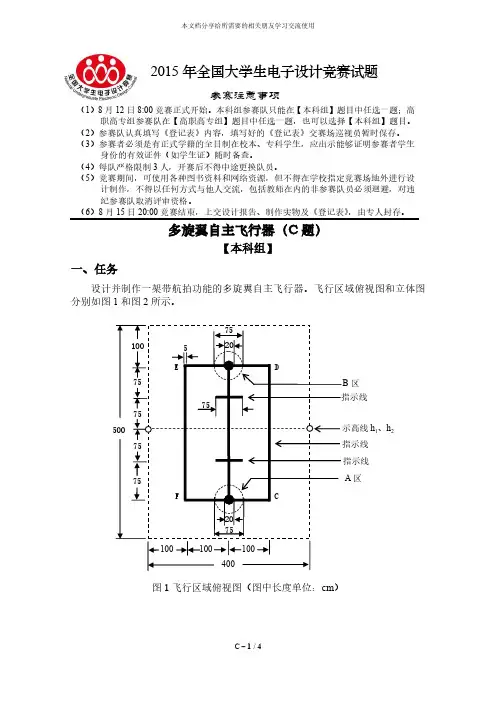
【本科组】一、任务设计并制作一架带航拍功能的多旋翼自主飞行器。
飞行区域俯视图和立体图分别如图1和图2所示。
图1飞行区域俯视图(图中长度单位:cm )A 区区h 1、h 2图2 飞行区域立体示意图(图中长度单位:cm )二、要求1. 基本要求(1)多旋翼自主飞行器(下简称飞行器)摆放在图1所示的A 区,开启航拍,一键式启动,飞行器起飞;飞向B 区,在B 区中心降落并停机;航拍数据记录于飞行器自带的存储卡中,飞行结束后可通过PC 回放。
飞行高度不低于30cm ;飞行时间不大于30s 。
(2)飞行器摆放在图1所示的A 区,一键式启动,飞行器起飞;沿矩形CDEF逆时针飞行一圈,在A 区中心降落并停机;飞行高度不低于30cm ;飞行时间不大于45s 。
(3)制作一个简易电子示高装置,产生示高线h 1、h 2 (如激光等),h 1、h 2位于同一垂直平面,飞行器触碰h 1、h 2线时该装置可产生声光报警。
示高线h 1、h 2的高度在测试现场可以调整。
调整范围为30cm~120cm 。
2. 发挥部分(1)飞行器摆放在A 区,飞行器下面摆放一小铁板M 1,一键式启动,飞行器拾取小铁板M 1并起飞。
飞行器携带小铁板M 1从示高线h 1、h 2间飞向B 区,并在空中将小铁板M 1投放到B 区中心;飞行器从示高线h 1、h 2间飞回A 区,在A 区中心降落并停机。
stm32f103芯片手册STM32F103是一款Cortex-M3内核的32位MCU芯片,由意法半导体(STMicroelectronics)公司生产。
该芯片具有低功耗、高计算性能和丰富的外设接口的特点,被广泛应用于各种应用领域。
下面是对STM32F103芯片手册的1000字简要介绍。
首先,STM32F103芯片具有强大的计算能力和丰富的存储器资源。
它采用了ARM Cortex-M3内核,主频可高达72MHz,同时支持单周期乘法和硬件除法指令,可快速执行复杂的算法。
此外,芯片内置了128KB或256KB的闪存和20KB的静态RAM,可以存储大量的程序代码和数据。
其次,STM32F103芯片提供了丰富的外设接口,能够满足各种应用需求。
它包括多个通用输入/输出(GPIO)引脚,可用于连接外部设备和传感器。
同时,芯片还提供了多个串行通信接口,如USART、SPI和I2C,可以与其他设备进行高速数据传输。
此外,芯片还支持多个定时器/计数器,用于实现精确的计时和定时功能。
第三,STM32F103芯片具有低功耗特性和丰富的电源管理功能。
它采用了多种节能技术,如待机模式、休眠模式和停机模式,可以最大限度地降低功耗。
同时,芯片还内置了多个电源管理模块,例如低功耗时钟、电压调整器和电池备份电源,以提供稳定可靠的电源供应。
最后,STM32F103芯片还提供了完善的开发工具和支持资源。
意法半导体提供了一整套的软件开发工具,包括Keil MDK和IAR Embedded Workbench等,可简化开发流程。
此外,芯片手册还详细介绍了芯片的引脚定义、寄存器配置、时钟设置、中断管理、外设控制等内容,为开发者提供了全面的技术支持。
综上所述,STM32F103芯片手册详细介绍了该芯片的技术规格、外设接口、低功耗特性和开发支持资源。
它具有强大的计算能力、丰富的存储资源和多样化的外设功能,适用于各种应用领域,如工业控制、智能家居、医疗设备等。
深圳市米电智控科技有限公司产品规格书产品名称:433M/315M无线接收芯片产品型号:RF500客户:确认:日期:1.概述RF500是一款高集成度超低功耗的单片ASK/OOK 射频接收芯片。
高频信号接收功能全部集成于片内以达到用最少的外围器件和最低的成本获得最可靠的接收效果。
因此它是真正意义上的“天线高频调制信号输入,数字解调信号输出”的单片接收器件。
工作电压范围2.0V~6V 和非常高的灵敏度-110dBm,以及超低的工作电流3mA@315MHz,使之非常适合各种低功耗要求的设备等。
芯片内自动完成所有的RF和IF调谐,所以在开发和生产中就省略了手工调节的工艺工程,进而降低成本,加快产品上市。
2.特性完美兼容SYN480R、RF480、PRO480完全的单片UHF接收器件频率范围:300MHz - 440 MHz工作电压:2.0V~5V中频滤波器带宽:430KHz低功耗模式:3mA (315MHz,完全工作)3.3mA (433.92MHz,完全工作)0.01uA (关断模式)接收灵敏度-109 dBm @ 315MHz-110 dBm @ 433MHz数据速率:最大传输速率10kbps,建议使用在2.5kbps以下标准的CMOS接口控制及解码数据输出RF天线辐射非常低最经济的外围器件设计方案集成度高、外围简单、稳定可靠上电稳定时间是指≥20ms(SHUTDOWN从1到0时,DO稳定输出需要的时间)3. 应用领域遥控扇遥控灯遥控门遥控键盘远距离RFID智能家居控制器遥控玩具无线加密设备接收器短距离遥控器4.典型应用RF500 315MHz 典型电路RF500 433.92MHz 典型电路注:1、RF500也可直接替代SYN480R。
如果使用以上外围元件则效果更佳。
2、对于5V的应用,电源容易达到芯片的临界工作电压。
此时需要在RF电源引脚上串入47欧姆电阻,以保护芯片。
3、在SHUTDOWN模式下,DO引脚处于弱下拉状态。
Open107V用户手册目录1. 硬件介绍 (2)1.1.资源简介 (2)2. 例程分析 (4)2.1. 8Ios (4)2.2. ADC+DMA (4)2.3. ADC+DMA+KEYPAD (5)2.4. CAN- Normal (5)2.5. DAC (6)2.6. ETH_LwIP (6)2.7. GPIO LED JOYSTICK (7)2.8. I2C (7)2.9. LCD (8)2.10. OneWire (9)2.11. PS2 (9)2.12. RTC (9)2.13. FATFS V0.08A-SD Card (10)2.14. SL811 USB (10)2.15. AT45DB-SPI (11)2.16. TouchPanel (11)2.17. uCOSII2.91+UCGUI3.90A (12)2.18. USART (13)2.19. USB_Host_HID_KBrd_Mouse (13)2.20. USB_ Host_MSC(efsl) (13)2.21. USB_Host_MSC(FATFS) (14)2.22. USB-JoyStickMouse (15)2.23. USB-Mass_Storage-MCU Flash (15)2.24. VS1003B (16)3. 版本修订 (16)1.硬件介绍1.1. 资源简介[ 芯片简介 ]1.STM32F107VCT6STM32功能强大,下面仅列出STM32F107VCT6的核心资源参数:内核:Cortex-M3 32-bit RISC;工作频率:72MHz,1.25 DMIPS/MHz;工作电压:2-3.6V;封装:LQFP100;I/O口:80;存储资源:256kB Flash,64kB RAM;接口资源:3 x SPI,3 x USART,2 x UART,2 x I2S,2 x I2C;1 x Ethernet MAC,1 x USB OTG,2 x CAN;模数转换:2 x AD(12位,1us,分时16通道),[ 其它器件简介 ]3."5V DC"或"USB"供电选择开关切换到上面,选择5V DC供电;切换到下面,选择USB供电。
yIndustry Standard Pinouty Internal SMD Construction y UL 94V-0 Package Material y Temperature Performance -40] to +75]y Output 5, 9, 12 and 15VDCy Input 5, 12 and 24VDC y Low Costy MTBF > 2,000,000 Hours y 3000VDC Isolationy Efficiency up to 79%Key Features1W, Ultra-Miniature, High Isolation, Single Output DC/DC ConvertersTaking up as little as 0.16 square inches of board space, Minmax's MFU100 1W DC/DC's are specially designed to provide power distribution applications where space is critical in an ultra-miniature DIP package.The series consists of 12 models with input voltages of 5V, 12V and 24VDC which offers standard single output voltages of 5V, 9V, 12V, 15VDC.The MFU100 series is an excellent selection for a variety of applications including distributed power systems, mixed analog/digital subsystems,portable test equipments, local power networks and battery backed systems.Exceeding the absolute maximum ratings of the unit could cause damage.These are not continuous operating ratings.Free-Air ConvectionCoolingmW450---Internal Power Dissipation%95---Humidity ]260---Lead Temperature (1.5mm from case for 10 Sec.)]+125-40Storage Temperature VDC 28-0.724VDC Input Models]+90-25CaseOperating Temperature VDC 15-0.712VDC Input Models ]+75-40Ambient Operating Temperature VDC 7-0.75VDC Input Models Input Surge Voltage( 1000 mS )Unit Max.Min.Conditions ParameterUnit Max.Min.ParameterEnvironmental SpecificationsAbsolute Maximum RatingsREV:4 2008/10MINMAX17945316715MFU125794531.58412MFU1247655421109MFU12370810604200524(21.6~26.4)MFU12279410616715MFU1157951061.58412MFU11477510721109MFU113719131174200512(10.8~13.2)MFU11278625716715MFU1057772621.58412MFU10476826021109MFU103691130290420055(4.5~5.5)MFU102% (Typ.)% (Max.)mA (Typ.)mA (Typ.)mA mA VDC VDC@Max. Load @No Load @Max. Load Min.Max.EfficiencyLoad RegulationInput CurrentOutput CurrentOutput VoltageInput VoltageModel NumberModel Selection GuideuF33333333Maximum Capacitive LoadUnit 15V 12V 9V 5V Models by Vout Capacitive Load100mA Slow - Blow Type200mA Slow - Blow Type500mA Slow - Blow Type24V Input Models 12V Input Models 5V Input Models Input Fuse Selection GuideInternal CapacitorInput FilterA 0.3------All ModelsReverse Polarity Input Current 26.42421.624V Input Models13.21210.812V Input Models VDC 5.554.55V Input Models Input Voltage RangeUnitMax.Typ.Min.Model ParameterInput Specifications0.5 Second Max.Output Short Circuit%/]{0.02{0.01---Temperature Coefficient mV rms 15------Ripple & Noise (20MHz)mV P-P 200------Over Line, Load & Temp.Ripple & Noise (20MHz)mV P-P 150100---Ripple & Noise (20MHz)%See Model Selection GuideIo=20% to 100%Load Regulation %{1.5{1.2---For Vin Change of 10%Line Regulation %{3.0{1.0---Output Voltage Accuracy Unit Max.Typ.Min.ConditionsParameterOutput Specifications2MINMAX REV:4 2008/10K Hours------2000MIL-HDBK-217F @ 25], Ground BenignMTBFKHz 1109050Switching Frequency pF 10060---100KHz,1VIsolation Capacitance M[------1000500VDC Isolation Resistance VDC ------3300Flash Tested for 1 SecondIsolation Voltage Test VDC ------300060 SecondsIsolation Voltage Rated Unit Max.Typ.Min.Conditions ParameterGeneral SpecificationsNotes:1. Specifications typical at Ta=+25], resistive load, nominal input voltage, rated output current unless otherwise noted.2. Ripple & Noise measurement bandwidth is 0-20 MHz.3. These power converters require a minimum output loading to maintain specified regulation.4. Operation under no-load conditions will not damage these modules; however, they may not meet all specifications listed.5. All DC/DC converters should be externally fused at the front end for protection.6. Other input and output voltage may be available, please contact factory.7. Specifications subject to change without notice.Block DiagramREV:4 2008/10MINMAX3Derating Curve ( All Other Output )Derating Curve ( 5V Output Only )]Ambient TemperatureO u t p u t P o w e r (%)20406080100-405060801001109070]Ambient TemperatureO u t p u t P o w e r (%)020*********-405060801001109070Efficiency vs Output Load4MINMAX REV:4 2008/10Test ConfigurationsInput Reflected-Ripple Current Test SetupInput reflected-ripple current is measured with a inductor Lin (4.7uH) and Cin (220uF, ESR < 1.0[ at 100 KHz) to simulate source impedance.Capacitor Cin, offsets possible battery impedance.Current ripple is measured at the input terminals of the module, measurement bandwidth is 0-500 KHz.Peak-to-Peak Output Noise Measurement TestUse a Cout 0.33uF ceramic capacitor.Scope measurement should be made by using a BNC socket, measurement bandwidth is 0-20 MHz. Position the load between 50 mm and 75 mm from the DC/DC Converter.Design & Feature ConsiderationsMaximum Capacitive LoadThe MFU100 series has limitation of maximum connected capacitance at the output.The power module may be operated in current limiting mode during start-up, affecting the ramp-up and the startup time.For optimum performance we recommend 33uF maximum capacitive load for devices.The maximum capacitance can be found in the data sheet.Input Source ImpedanceThe power module should be connected to a low ac-impedance input source. Highly inductive source impedances can affect the stability of the power module.In applications where power is supplied over long lines and output loading is high, it may be necessary to use a capacitor at the input to ensure startup.Capacitor mounted close to the power module helps ensure stability of the unit, it is recommended to use a good quality low Equivalent Series Resistance (ESR < 1.0[ at 100KHz) capacitor of a 1.5uF for the 5V input devices, a 1.0uF for the 12V input devices and a 0.47uF for the 24V devices.Output Ripple ReductionA good quality low ESR capacitor placed as close as practicable across the load will give the best ripple and noise performance.To reduce output ripple, it is recommended to use 1uF capacitors at the output.Thermal ConsiderationsMany conditions affect the thermal performance of the power module, such as orientation, airflow over the module and board spacing. To avoid exceeding the maximum temperature rating of the components inside the power module, the case temperature must be kept below 90°C.The derating curves are determined from measurements obtained in an experimental apparatus.REV:4 2008/10MINMAX51.7g (24V Input)1.3g (5 & 12V Input):WeightNon-Conductive Black Plastic :Case Material0.50*0.31*0.40 inches 12.7*8.0*10.16 mm :Case Size (24V Input)0.50*0.28*0.40 inches 12.7*7.0*10.16 mm :Case Size(5V & 12V Input)Physical CharacteristicsMechanical Dimensions-Vout7+Vout 5+Vin 4-Vin 1Function Pin Pin Connections{0.002{0.05PinX.XXX{0.005X.XX{0.13X.XX{0.01X.X{0.25Inches Millimeters Tolerance6MINMAX REV:4 2008/10。
stm32f103英文手册
对不起,我无法直接为您提供STM32F103的英文手册。
但我可以给您一些关于STM32F103的信息和如何找到该手册的建议。
STM32F103是STMicroelectronics生产的一款基于ARM Cortex-M3的
微控制器。
其特点包括:
1. 512KB Flash内存
2. 64KB SRAM
3. 7个定时器
4. 3个ADC
5. 2个DAC
6. 10个通信接口(包括I2C,SPI,UART等)
7. 实时时钟
8. 温度传感器
9. 欠压检测器
10. 定时器PWM输出
您可以在STMicroelectronics的官方网站上找到STM32F103的完整手册。
通常,这些手册都是以PDF格式提供的,可以轻松下载和阅读。
您可以在
搜索引擎中输入“STM32F103 datasheet”或“STM32F103 reference manual”来找到该手册。
如果您遇到任何困难或问题,例如找不到所需的手册或无法理解其中的内容,我建议您在STMicroelectronics的官方论坛或相关社区中寻求帮助。
那里
有许多经验丰富的用户和开发者,他们愿意分享他们的知识和经验。
CMS32M55xx 数据手册ARM ® Cortex ® -M0 32位电机微控制器 Rev. 1.08请注意以下有关CMS 知识产权政策*中微半导体(深圳)股份有限公司(以下简称本公司)已申请了专利,享有绝对的合法权益。
与本公司MCU或其他产品有关的专利权并未被同意授权使用,任何经由不当手段侵害本公司专利权的公司、组织或个人,本公司将采取一切可能的法律行动,遏止侵权者不当的侵权行为,并追讨本公司因侵权行为所受的损失、或侵权者所得的不法利益。
*中微半导体(深圳)股份有限公司的名称和标识都是本公司的注册商标。
*本公司保留对规格书中产品在可靠性、功能和设计方面的改进作进一步说明的权利。
然而本公司对于规格内容的使用不负责任。
文中提到的应用其目的仅仅是用来做说明,本公司不保证和不表示这些应用没有更深入的修改就能适用,也不推荐它的产品使用在会由于故障或其它原因可能会对人身造成危害的地方。
本公司的产品不授权适用于救生、维生器件或系统中作为关键器件。
本公司拥有不事先通知而修改产品的权利,对于最新的信息,请参考官方网站 。
1. 产品特性1.1 MCU功能特性◆内核ARM Cortex™-M0,**********~5.5V- 单周期32位硬件乘法器◆32位硬件除法器(HWDIV)- 有/无符号模式,6个HCLK完成运算◆存储器- 最大32K字节程序FLASH(APROM+BOOT)- 1K字节的FLASH数据区(独立空间)- 最大8K字节SRAM(支持分区写保护功能)- 支持BOOT功能,BOOT区可设置大小0-4K- 支持硬件CRC校验FLASH空间代码- 支持FLASH分区保护(最小单位为2K)◆系统时钟- 内部高速振荡48MHz/64MHz(HSI)- 内部低速振荡40KHz(LSI)◆GPIO(最多24 I/Os)◆LVR(1.9V/2.1V/2.6V)◆LVD(2.0V/2.2V/2.4V/2.7V/3.0V/3.7V)◆系统定时器- 24位SysTick定时器- 看门狗定时器(WDT)- 窗口看门狗定时器(WWDT)◆正常模式/睡眠模式/深度睡眠模式/停止模式◆通用循环冗余校验单元(CRC)◆定时器(32bit/16bit-TIMER0/1)◆捕获/比较/脉宽调制(CCP0/1)- 支持4通道同时捕捉可连接到霍尔传感器接口◆通信接口- 1个I2C模块(通信速度最快可达1Mb/s)- 1个SSP/SPI模块(4-16位数据格式可调)- 最多2个UART:UART0/1(共32个收/发FIFO)(UART1的TXD1与RXD1可分配到任意端口)◆串行调试接口SWD(2-Wire)◆96bit唯一ID(UID)◆128bit用户UID(USRUID)- 用户可设置,可加密(可作为安全密钥)◆增强型PWM(EPWM)- 6路通道且通道可重映射- 支持独立/互补/同步/成组输出模式- 支持边沿/中心对齐计数模式- 支持单次/连续/间隔加载更新模式- 支持互补模式插入死区延时- 支持掩码及掩码预设(共8个掩码状态缓存)- 支持霍尔传感器接口(硬件控制PWM输出)- 支持硬件刹车及6种刹车信号源◆ADC0(12bit,100Ksps)- 最多24个输入通道- 每个转换通道有独立的结果寄存器- 支持单次/连续模式- 支持2种硬件触发方式共7个触发源- 1个转换结果比较器,可产生中断◆ADC1(12bit,1.2Msps)- 最多24个输入通道- 每个转换通道有独立的结果寄存器- 支持单次/连续模式/插入模式- 支持外部触发方式- 1个转换结果比较器,可产生中断◆模拟比较器(ACMP0/1)- 正端4路选择,负端可选内部1.2V/VDD分压- 支持迟滞电压选择:10mV/20mV/60mV- 支持比较器输出触发EPWM刹车◆可编程增益放大器(PGA0/1)- 正端4路选择- 输出可接内部ADC通道与模拟比较器的输入- 内部增益可选择:4倍~32倍◆运算放大器(OP0/1)- 输入可接内部1.2V基准- 输出可接内部ADC通道与模拟比较器的输入- 可设置为比较器模式◆支持安全相关的功能与应用- 满足IEC60730 CLASS B 标准1.2 产品对比以下是CMS32M55XX芯片的产品对比注:1) 通过系统配置寄存器设置APROM和BOOT空间大小,APROM与BOOT空间总共最大为32K;2) 表示模拟模块个数,模拟功能并非通过管脚的输入/输出实现,输入/输出管脚以实际产品为准。
芯海科技产品手册CHIPSEA PRODUCT MANUAL芯海科技成立于2003年9月,是一家集感知、计算、控制、连接于一体的全信号链集成电路设计企业。
专注于高精度ADC、高可靠性MCU、测量算法以及AIoT 一站式解决方案的研发设计。
产品和方案广泛应用于工业测量与工业控制、通信与计算机、锂电管理、消费电子、汽车电子、智慧家居、智能仪表、智慧健康等领域。
公司总部位于深圳,在合肥、西安、上海、成都设立子公司,是国家级高新技术企业,被广东省科技厅认定为“广东省物联网芯片开发与应用工程技术研究中心”,获得国家级专精特新“小巨人”称号。
建有可靠性检测中心、健康测量实验室、感知实验室、MCU实验室。
公司年均研发投入超过20%,研发人员占比近70%,核心成员均有10年以上工作经验。
截止到2022年上半年,芯海科技累计拥有全球专利申请近800件,累计拥有已授权专利近350件(含美国专利),拥有专利数量在科创板芯片设计上市公司中名列前茅。
企业简介ABOUT CHIPSEA1523健康测量信号调理数据转换器模拟前端32位MCU 8位MCU010406091113信号链无线产品低功耗蓝牙开发生态开发生态鸿蒙智联解决方案OKOK智能物联解决方案健身行业SaaS 解决方案2021221719电源管理AIoT产品快 充电池管理MCUC H I P S E A32位MCU系列产品概述芯海科技的CS32系列32位MCU基于Arm®Cortex®-M处理器,内嵌Flash存储器,集成高精度ADC和丰富的模拟外设。
该产品系列品类齐全,同时保持了集成度高和易于开发的特点,提供了丰富的软件和开发工具支持,广泛应用于工业控制、汽车电子、智能家居、消费类电子等领域。
产品特色典型应用高可靠低功耗高精度32KB64KB 128KB 256KB 512KB 1024KB ��TWS电子烟电表电动自行车扫地机器人无人机C H I P S E A 产品选型C H I P S E AC H I P S E A8位MCU系列产品概述芯海科技的8位MCU采用芯海科技自主知识产权的8位RISC内核,并集成12位ADC、内部基准电压、OTP或Flash存储器、PWM等资源,支持C语言开发,具有低功耗、易开发等特点。
新唐单⽚机最全选型表NuMicro? 单⽚机家族1Mini51 Base Series ⾼集成、低价位、低管脚、⾼性能32位微控制器Contact us: NuMicro@/doc/84abc79a6edb6f1afe001f27.htmlNuMicro? 单⽚机家族Mini51 系列NuMicro ? 是新唐科技新⼀代32位微控制器,采⽤ARM 公司低功耗、具精简指令代码特性的Cortex ?-M0与Cortex ?-M4处理器为核⼼,适合⼴泛的微控制器应⽤领域。
NuMicro ? Cortex ?-M0家族⽬前已量产系列有:NUC100系列与NUC200系列;带有USB 2.0全速设备的低功耗NUC120/NUC122/NUC123系列与NUC220系列;内嵌最多2組CAN 总线NUC130/131/140与NUC230/240系列;⾼性价⽐的M051/M0518系列;低管脚、低价位的Mini51系列;超低功耗运⾏的Nano100/102/112系列,0.65uA (待機功耗,内存数据保存),内嵌LCD 驱动 Nano110/112 系列, USB 2.0全速设备的超低功耗Nano120系列;⾼整合度 LCD 驱动与USB 2.0全速设备的超低功耗 Nano130系列。
Cortex ?-M4家族之⾼性能NUC442/472系列,其包含丰富外设,如以太⽹、USB OTG 和⾼速设备、双CAN 总线等等;具⾼整合度的M451系列,其带有USB OTG 和全速设备,CAN 总线,可调电压接⼝(VAI),⾼分辨率PWM 。
NuMicro ?家族的Cortex ?-M0与Cortex ?-M4微处理器为各种应⽤提供了32位最佳的性价⽐选择。
NuMicro ? Mini51系列为32位单⽚机,内建ARM ? Cortex ?-M0 内核最⾼可运⾏⾄24MHz ,具4K/8K/16K 字节Flash 内存、2K 字节内建SRAM 、可配置的数据Flash(与程序Flash 内存共享)、2K 独⽴Flash 字节作为在线系统编程(In System Programming)⽤途。
MM 32 FMM 32 SPINMM 32 PMM 32 L MM 32 W通用高性能微控制器产品电机与电源专用微控制器产品超精简型微控制器产品低功耗高安全微控制器产品无线微控制器产品公司概况|Company Overview灵动微电子成立于2011年,是中国本土领先的通用32位MCU产品及解决方案供应商。
灵动微电子的MCU 产品以MM32为标识,基于Arm Cortex-M系列内核,自主研发软硬件和生态系统。
目前已量产200多款型号,累计交付超2亿颗,在本土通用32位MCU公司中位居公司介绍灵动产品家族前列。
客户涵盖智能工业、汽车电子、通信基建、医疗健康、智慧家电、物联网、个人设备、手机和电脑等应用领域。
灵动微电子是中国为数不多的同时获得了Arm-KEIL、IAR、SEGGER国际权威组织官方支持的本土MCU公司,并建立了独立、完整的通用MCU生态体系,可以为客户提供从硬件芯片到软件算法、从参考方案到系统设计的全方位支持。
灵动微电子的MM32系列有5大家族:面向通用高性能MCU市场领域MM 32 F提供开放式的无线平台MM 32 W专用于电机和电源应用MM 32 SPIN支持超精简定制化需求MM 32 P覆盖低功耗、安全应用场景MM 32 L01公司概况|Company OverviewMM32 产品组合|MM32 MCU Product Portfolio02MM32 产品组合|MM32 MCU Product PortfolioMM32F通用系列MM32L低功耗系列MM32W无线系列MM32SPIN电机与电源系列全新MM32|New MM32全新MM32系列是灵动微电子于2020年推出的新一代通用MCU平台,旨在为客户提供更高性能、更低功耗、更高可靠性、稳定性和健壮性的微控制器。
全新MM32硬件上与经典MM32全兼容,保留了2.0-5.5V 宽压供电设计。
- 高性能Arm Cortex-M0 (高达96MHz)和 Arm Cortex-M3- Flash: 16KB - 512KB, SRAM: 2KB - 128KB - 不同系列之间引脚兼容,提供 20/32/48/ 64/100/144 多种引脚和封装形式产品特点MM32F 系列是灵动微电子新一代 MM32系列中率先升级推出的通用高性能MCU 平台。
Key Featuresl SMT Technologyl Miniture Packagel I / O Isolation 1000VDCl Efficiency Up To 80%l MTBF > 2,000,000 Hoursl Low CostMechanical ConfigurationmW450---Internal Power DissipationVDC 30-0.724VDC Input ModelsVDC 18-0.712VDC Input Models VDC 9-0.75VDC Input Models Input Surge Voltage( 1000 mS )Unit.Max.Min.ParameterAbsolute Maximum RatingsExceeding these values can damage the module.These are not continuous operating ratings.Internal CapacitorInput FilterA0.3------All ModelsReverse Polarity Input Current 26.42421.624V Input Models13.21210.812V Input Models VDC 5.554.55V Input Models Input Voltage RangeUnit Max.Typ.Min.Model ParameterInput SpecificationsSpecifications typical at Ta=+25],resistive load,nominal input voltage,rated output current unless otherwise noted.7945316715MBU118794531.58412MBU1177655421109MBU116708 7604200524(21.6 ~ 26.4)MBU11580410516715MBU1147951061.58412MBU11377510721109MBU112719131174200512(10.8 ~ 13.2)MBU11178625816715MBU1047772621.58412MBU10376826021109MBU102691130290420055(4.5 ~ 5.5)MBU101Efficiency % (Typ.)Load Regulation % (Max.)Input Current No Load mA (Typ.)Input Current Max. Load mA (Typ.)Output Current mA (Min.)Output Current mA (Max.)Output Voltage VDC Input voltage VDCModel NumberModel Selection GuideFree-Air ConvectionCooling%95------Humidity ]+125----40Storage Temperature ]+75----25Operating Temperature Unit Max.Typ.Min.ConditionsParameterEnvironmental SpecificationsTypical ApplicationsConnecting Pin Patterns(2.54 mm / 0.1 inch grids )kHz1109050Switching FrequencypF 10060---100KHz,1VIsolation Capacitance M[------1000500VDC Isolation Resistance VDC ------100060 Seconds Rated Isolation Voltage Unit Max.Typ.Min.Conditions ParameterGeneral Specification0.5 Second Max.Output Short Circuit%/]{0.02{0.01---Temperature Coefficient %------120Over LoadmV rms.5------Ripple & Noise (20MHz)mV P-P 200------Over Line,Load & Temp.Ripple & Noise (20MHz)mV P-P 150100---Ripple & Noise (20MHz)%See Model Selection GuideIo=20% to 100%Load Regulation %{1.5{1.2---For Vin Change 1%Line Regulation %{3.0{1.0---Output Voltage Accuracy Unit Max.Typ.Min.ConditionsParameterOutput Specifications100mA Slow - Blow Type200mA Slow - Blow Type500mA Slow - Blow Type24V Input Models 12V Input Models 5V Input ModelsInput Fuse Selection GuideDerating Curve5V Output OnlyAll Other OutputNOTE:1. Specifications typical at Ta=+25],resistive load,nominal input voltage,rated output current unless otherwise noted.2. Other input and output voltage may be available,Please contact factory.3. Specifications subject to change without notice.。
PIC10F20X6-Pin, 8-Bit Flash Microcontroller一、PIC10F Family 介绍1.基本的特点---仅33条指令,12-bit宽度指---除程序支跳转指令为双周期指令外,其余所有指令皆为单周期指令---2级硬件堆栈---直接、间接和相对寻址模式---8-bit数据宽度---8个特殊功能寄存器---精确的内部4 MHz 振荡器–4MHz 1% 3.0V, 25°C–4MHz 2% 2.5V-5.5V, 0°C - + 85°C–4MHz 5% 2.0V-5.5V, -40°C - +125°C---在线编程(ICSP)---在线调试(ICD)---每个I/O口有25 mA的拉/灌电流---上电复位(POR)--复位时间(DRT)---看门狗定时器(WDT)---低功耗的睡眠电流(100nA)---一个8-bit定时器(TMR0)---可编程代码保护---引脚电平变化唤醒睡眠2.PIC10F FamilyPIC10F Device-Specific FeaturesDevice Program Flash(Words) Data RAMInternalOSC ComparatorPIC10F200 256 16 Yes -PIC10F202 512 24 Yes -PIC10F204 256 16 Yes 1PIC10F206 512 24 Yes 1 Device Block DiagramDevice Block Diagram TermsPrecision Internal Oscillator I内部的4Mhz 系统时钟,精度可达到+/- 1% Special Function Registers 特殊功能寄存器常被用于配置、控制外围接口和CPU的操作Data RAM 随机数据的访问存取Instruction Decode 程序执行时解析操作码和操作数Flash Program Memory 程序存储器I/O Drivers and Controls 控制输入输出的电路和寄存器COMP 比较器W Register W寄存器Program Counter and Stack 程序计数指针指向下一条指令地址;10位的堆栈寄存器,不可寻址。
1. InstallationDo not connect the E1 debugger module until the software support has been installed.1.Insert the CD into your computer’s CD-ROM drive. The CD should automatically run the installation program.If the installer does not start, browse to the CD root folder and double click on ‘CsPlusLauncher.exe’.2.Windows™ Vista/Windows™ 7 users may see “User Account Control” dialog box. If applicable, enter theadministrator password and click <OK>.3.The pre installer will first check to see if the CubeSuite prerequisites are present, and will install if necessary(this may take a few minutes).4.Once the prerequisites are setup, the CubeSuite+ installer will launch.5.The CubeSuite+ Welcome window will appear. Click <Next>.6.The End User License Agreement appears. Read the license agreement and select <Accept> if you wish tocontinue. Click <Next>.7.The ‘Select Component’ window appears. Review the components by selecting each component in turn.Click <Next> to continue.8.The License Key Registration window appears. If you have a license key available, click the <LicenseManager> button, otherwise go to Step 9. Enter the license key in the opened ‘License Manager’ dialog. Add the license key. Click <Add>. If the license key is added successfully, click <Close>.9.Click <Next>.10.The ‘Installation Settings Confirmation’ window appears. Review the information and click <Next> to begininstallation.11.The ‘Installation Execution’ window will appear showing the install status progress. Before completion, theRenesas E-Series USB Driver installation dialog will appear. Windows™ Vista and Windows™ 7 users may see a ‘Windows Security’ dialog box. Click ‘Always trust software from “Renesas Solutions Corp.”’ then click <Install>. 12.After a successful installation click <Next>.13.The ‘Setup Completion’ window will appear. Click <Finish> to close the installer.2. Connection14.Fit the LCD module to the connector marked ‘LCD’ on the RSK. Ensure all the pins of the connector arecorrectly inserted in the socket.15.Connect the E1 debugger module to the connector marked ‘E1’ on the RSK using the ribbon cable.16.Connect the E1 debugger module to a spare USB port of your PC. The green ‘ACT’ LED on the E1 debuggerwill flash.17.The ‘Found New Hardware’ Wizard will appear. Please follow the steps below to install the drivers. Note that,administrator privileges are required for a Windows™ XP/Vista machine.Windows™ XP Windows™ Vista / Windows™ 7a.Select option ‘No, not this time’ in “Found NewHardware” Wizard dialog, and click <Next>button.a.“Device driver software installed successfully”pop-up will appear in the Windows toolbar andinstallation will complete.b.Verify the “Recommended” option is selectedand click <Next>.c.If using Windows™ XP, go to step ‘e’;otherwise, click <Next>.d.Click <Next> to install the driver.e.Click <Finish> to close the wizard.Note: The Windows driver signing dialog may be displayed. Please accept the driver to continue.18.The green ‘ACT’ LED on the E1 debugger will illuminate.3. CubeSuite+ ProjectCubeSuite+ integrates various tools such as compiler, assembler, debugger and editor into a common graphical user interface. To learn more on how to use CubeSuite+, refer to the CubeSuite+ Tutorial manual from the menu bar (Help > Tutorial).unch CubeSuite+ from the Windows Start Menu. (Start Menu > All Programs > Renesas ElectronicsCubeSuite+ > CubeSuite+).20.The ‘One Point Advice’ dialog which provides useful tips will open. The detail for this is out of scope for thisguide. Click <OK>.21.The Start panel will appear. Select the RSKRL78G13_Tutorial project under the “Open Sample RSK Project”and click <GO>.22.In the “Create Project” dialog that follows, specify a name for the project. Leave the list of subprojectsunselected.23.Click “Create” to launch the main Tutorial project.4. Programming and Debug24. Click on RL78 Simulator (Debug Tool) from the Project Tree pane and select the “RL78 E1 (Serial)” asshown in the following screenshot:25. Right-click on “RL78 E1(Serial) (Debug Tool)” and select ‘Property’.26. On the ‘Property’ tab, select “Power target from the emulator.(MAX200mA)”.27. Click on the drop-down menu button on the right and select “Yes”. A new entry, “Supply voltage”, will appear. 28.Click on the “Supply voltage” entry and change the voltage to 5.0V from the drop-down menu.29.Build the project by clicking on the Build Project button.30.Download the code to the microcontroller by clicking on the download buttonor click on Debug from the Menu bar and click on Download as shown below:31.Click the <Restart> button to reset the CPU then start program execution.The user LEDs on the board will flash at regular intervals. Pressing any of the switches on the RSK, or after 200 flashes have elapsed, will display the string STATIC on the second line of the debug LCD. The second line will then be replaced with the string TESTTEST one character at a time; whilst allowing you to control the user LEDs’ flashing rate using the potentiometer shaft. 32.Click the <Stop> button.The code will stop and the source code will be opened at the current program counter.5. Next StepAfter you have completed this quick start procedure, please review the tutorial code and sample code that came with the kit. You can review these codes by changing the active project to another project. The tutorials will help you understand the device and development process using Renesas Development Tools.The Hardware manual supplied with this RSK is current at the time of publication. Please check for any updates to the device manual from the Renesas internet site at: /rskrl78g136. Renesas RL78 CompilerThe version of the compiler provided with this RSK is fully functional with no time restrictions. The compiler will limit the code linker to 64k bytes. Full licensed RL78 compiler versions are available from your Renesas supplier.7. User ManualsUser manuals can found in the Windows Start Menu. (Start Menu > All Programs > Renesas ElectronicsCubeSuite+ > Readme Documents > RSK > RSKRL78G13).8. SupportOnline technical support and information is available at: /rskrl78g13 Technical Contact Details csc@Note on Update Manager : The Update Manager checks via Internet for any updated resources available for each installed CubeSuite+ tool and downloads them accordingly to simplify the update process. Automatic updates will not work if CubeSuite+ is installed without a license key.© 2011 Renesas Electronics Europe Limited. All rights reserved. © 2011 Renesas Electronics Corporation. All rights reserved. © 2011 Renesas Solutions Corp. All rights reserved. Website: D010234_11_S01_V01。