中原2007年长沙市奥林匹克花园北京西院解筹开盘报告-PPT精品课程
- 格式:ppt
- 大小:4.26 MB
- 文档页数:67

XX奥林匹克花园项目报告项目位于湘府中路(天心区政府新址斜对面),东接韶山南路,西连芙蓉南路,与省政府,天心区政府隔路相望。
他由中体产业集团与本土湘天集团共同投资精心打造.主要经济技术指标总占地面积344465㎡㎡总建筑面积556663㎡住宅面积约400000㎡总户数3000容积率1.7绿化率43.67%户车比1.1主力户型三房两厅1.2 项目优势(Strength)分析品牌优势:依靠“奥林匹克花园”已在全国树立的深入人心的地产品牌强势进军XX房地产业,相当容易受到广大购房者的关注和亲睐。
加之中建五局,合富辉煌,中航物业的加盟,强强联合增强品牌集聚力。
规划优势:城南板块为新兴中心城市中心,高起点,高规划的城市定位,发展潜力巨大。
地段优势:紧邻XX省政府、天心区政府等政府职能部门,处于XX市市政中心地段;项目地段交通发达,周边主干道路:芙蓉南路、韶山南路等,雄踞于“长株潭一体”的重点发展地段。
资金优势:XX奥林匹克花园与XX兴业银行的合作,得此强助,如虎添翼。
同时也给正在热销的XX奥林匹克花园“锦上添花”,如同给目标客户、潜在客户吃了一颗“定心丸”。
资源优势:依靠XX省政府、天心区政府等政府职能部门带动片区发展,XX规划“长株潭一体”,规划CPD,市政配套,街区服务中心等城市资源将优化组合。
配套优势:项目周边配套设施日趋完善,已有配套XX市中心医院,汽车南站,南郊公园,植物园;规划中的配套省科技馆、青少年活动中心、文化艺术馆等大型公建配套设施外;项目自身配套运动MALL、五星级酒店、风情商业街、国际公寓、购物中心、大型超市等商业生活配套以及儿童公园,青少年羽毛球学校等教育设施配套。
园林优势:接近2万平米的文化广场,组团园林与5.2米架空层园林的结合提高项目的整体形象与配套。
户型优势:三房两厅面积112-122㎡的主力户型设计迎合众多购房者的心理需求面积。
板式设计坐北朝南、户型布局合理、实用率高;入户花园,凸窗设计,增大室内空间。
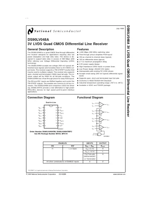
DS90LV048A3V LVDS Quad CMOS Differential Line ReceiverGeneral DescriptionThe DS90LV048A is a quad CMOS flow-through differential line receiver designed for applications requiring ultra low power dissipation and high data rates.The device is de-signed to support data rates in excess of 400Mbps (200MHz)utilizing Low Voltage Differential Signaling (LVDS)technology.The DS90LV048A accepts low voltage (350mV typical)dif-ferential input signals and translates them to 3V CMOS out-put levels.The receiver supports a TRI-STATE ®function that may be used to multiplex outputs.The receiver also supports open,shorted and terminated (100Ω)input fail-safe.The re-ceiver output will be HIGH for all fail-safe conditions.The DS90LV048A has a flow-through pinout for easy PCB layout.The EN and EN *inputs are ANDed together and control the TRI-STATE outputs.The enables are common to all four re-ceivers.The DS90LV048A and companion LVDS line driver (eg.DS90LV047A)provide a new alternative to high power PECL/ECL devices for high speed point-to-point interface applications.Featuresn >400Mbps (200MHz)switching ratesn Flow-through pinout simplifies PCB layout n 150ps channel-to-channel skew (typical)n 100ps differential skew (typical)n 2.7ns maximum propagation delay n 3.3V power supply designn High impedance LVDS inputs on power down n Low Power design (40mW 3.3V static)n Interoperable with existing 5V LVDS driversn Accepts small swing (350mV typical)differential signal levelsn Supports open,short and terminated input fail-safe n Conforms to ANSI/TIA/EIA-644Standardn Industrial temperature operating range (-40˚C to +85˚C)nAvailable in SOIC and TSSOP packageConnection DiagramFunctional DiagramENABLESINPUTS OUTPUT EN EN*R IN+−R IN−R OUT HL or OpenV ID ≥0.1V H V ID ≤−0.1V L Full Fail-safe OPEN/SHORT or TerminatedHAll other combinations of ENABLE inputs X ZTRI-STATE ®is a registered trademark of National Semiconductor Corporation.Dual-in-LineDS100888-1Order Number DS90LV048ATM,DS90LV048ATMTCSee NS Package Number M16A,MTC16July 1999DS90LV048A 3V LVDS Quad CMOS Differential Line Receiver©1999National Semiconductor Corporation Absolute Maximum Ratings(Note1)If Military/Aerospace specified devices are required, please contact the National Semiconductor Sales Office/ Distributors for availability and specifications.Supply Voltage(V CC)−0.3V to+4V Input Voltage(R IN+,R IN−)−0.3V to3.9V Enable Input Voltage(EN,EN*)−0.3V to(V CC+0.3V) Output Voltage(R OUT)−0.3V to(V CC+0.3V) Maximum Package Power Dissipation+25˚CM Package1025mW MTC Package866mW Derate M Package8.2mW/˚C above+25˚C Derate MTC Package 6.9mW/˚C above+25˚C Storage Temperature Range−65˚C to+150˚C Lead Temperature Range Soldering(4sec.)+260˚C Maximum Junction Temperature+150˚C ESD Rating(Note10)(HBM,1.5kΩ,100pF)≥10kV (EIAJ,0Ω,200pF)≥1200VRecommended Operating ConditionsMin Typ Max Units Supply Voltage(V CC)+3.0+3.3+3.6V Receiver Input Voltage GND+3.0V Operating Free AirTemperature(T A)−4025+85˚CElectrical CharacteristicsOver Supply Voltage and Operating Temperature ranges,unless otherwise specified.(Notes2,3)Symbol Parameter Conditions Pin Min Typ Max Units V TH Differential Input High Threshold V CM=+1.2V,0.05V,2.95V(Note13)R IN+,+100mV V TL Differential Input Low Threshold R IN−−100mV VCMR Common-Mode Voltage Range VID=200mV pk to pk(Note5)0.1 2.3V I IN Input Current V IN=+2.8V V CC=3.6V or0V−10±5+10µAV IN=0V−10±1+10µAV IN=+3.6V V CC=0V-20±1+20µA V OH Output High Voltage I OH=−0.4mA,V ID=+200mV R OUT 2.7 3.3VI OH=−0.4mA,Input terminated 2.7 3.3VI OH=−0.4mA,Input shorted 2.7 3.3V V OL Output Low Voltage I OL=2mA,V ID=−200mV0.050.25V I OS Output Short Circuit Current Enabled,V OUT=0V(Note11)−15−47−100mA I OZ Output TRI-STATE Current Disabled,V OUT=0V or V CC−10±1+10µAV IH Input High Voltage EN,EN*2.0V CC VV IL Input Low Voltage GND0.8V I I Input Current V IN=0V or V CC,Other Input=V CC orGND−10±5+10µA V CL Input Clamp Voltage I CL=−18mA−1.5−0.8V I CC No Load Supply CurrentReceivers EnabledEN=V CC,Inputs Open V CC915mA I CCZ No Load Supply Current EN=GND,Inputs Open15mAReceivers DisabledSwitching CharacteristicsOver Supply Voltage and Operating Temperature ranges,unless otherwise specified.(Notes3,4,7,8)Symbol Parameter Conditions Min Typ Max Units t PHLD Differential Propagation Delay High to Low C L=15pF 1.2 2.0 2.7ns t PLHD Differential Propagation Delay Low to High V ID=200mV 1.2 1.9 2.7ns t SKD1Differential Pulse Skew|t PHLD−t PLHD|(Note6)(Figure1and Figure2)00.10.4ns t SKD2Differential Channel-to-Channel Skew;same device(Note7)00.150.5ns t SKD3Differential Part to Part Skew(Note8) 1.0ns t SKD4Differential Part to Part Skew(Note9) 1.5ns t TLH Rise Time0.5 1.0ns t THL Fall Time0.35 1.0ns 2Switching Characteristics(Continued)Over Supply Voltage and Operating Temperature ranges,unless otherwise specified.(Notes3,4,7,8)Symbol Parameter Conditions Min Typ Max Units t PHZ Disable Time High to Z R L=2kΩ814nst PLZ Disable Time Low to Z C L=15pF814nst PZH Enable Time Z to High(Figure3and Figure4)914nst PZL Enable Time Z to Low914nsf MAX Maximum Operating Frequency(Note14)All Channels Switching200250MHzNote1:“Absolute Maximum Ratings”are those values beyond which the safety of the device cannot be guaranteed.They are not meant to imply that the devices should be operated at these limits.The table of“Electrical Characteristics”specifies conditions of device operation.Note2:Current into device pins is defined as positive.Current out of device pins is defined as negative.All voltages are referenced to ground unless otherwise speci-fied.Note3:All typicals are given for:V CC=+3.3V,T A=+25˚C.Note4:Generator waveform for all tests unless otherwise specified:f=1MHz,Z O=50Ω,t r and t f(0%to100%)≤3ns for R IN.Note5:The VCMR range is reduced for larger VID.Example:if VID=400mV,the VCMR is0.2V to2.2V.The fail-safe condition with inputs shorted is not supported over the common-mode range of0V to2.4V,but is supported only with inputs shorted and no external common-mode voltage applied.A VID up to V CC−0V may be applied to the R IN+/R IN−inputs with the Common-Mode voltage set to V CC/2.Propagation delay and Differential Pulse skew decrease when VID is increased from 200mV to400mV.Skew specifications apply for200mV≤VID≤800mV over the common-mode range.Note6:t SKD1is the magnitude difference in differential propagation delay time between the positive going edge and the negative going edge of the same channel Note7:t SKD2,Channel-to-Channel Skew is defined as the difference between the propagation delay of one channel and that of the others on the same chip with any event on the inputs.Note8:t SKD3,part to part skew,is the differential channel-to-channel skew of any event between devices.This specification applies to devices at the same V CC, and within5˚C of each other within the operating temperature range.Note9:t SKD4,part to part skew,is the differential channel-to-channel skew of any event between devices.This specification applies to devices over recommended operating temperature and voltage ranges,and across process distribution.t SKD4is defined as|Max−Min|differential propagation delay.Note10:ESD Rating:HBM(1.5kΩ,100pF)≥10kVEIAJ(0Ω,200pF)≥1200VNote11:Output short circuit current(I OS)is specified as magnitude only,minus sign indicates direction only.Only one output should be shorted at a time,do not exceed maximum junction temperature specification.Note12:C L includes probe and jig capacitance.Note13:V CC is always higher than R IN+and R IN−voltage.R IN−and R IN+are allowed to have a voltage range−0.2V to V CC−VID/2.However,to be compliant with AC specifications,the common voltage range is0.1V to2.3VNote14:f MAX generator input conditions:t r=t f<1ns(0%to100%),50%duty cycle,differential(1.05V to1.35V peak to peak).Output criteria:60/40%duty cycle, V OL(max0.4V),V OH(min2.7V),Load=15pF(stray plus probes).Parameter Measurement InformationDS100888-3FIGURE1.Receiver Propagation Delay and Transition Time Test CircuitDS100888-4FIGURE2.Receiver Propagation Delay and Transition Time Waveforms3Parameter Measurement Information(Continued)Typical ApplicationApplications InformationGeneral application guidelines and hints for LVDS drivers and receivers may be found in the following application notes:LVDS Owner’s Manual (lit #550062-001),AN808,AN977,AN971,AN916,AN805,AN903.LVDS drivers and receivers are intended to be primarily used in an uncomplicated point-to-point configuration as is shown in Figure 5.This configuration provides a clean signaling en-vironment for the fast edge rates of the drivers.The receiver is connected to the driver through a balanced media which may be a standard twisted pair cable,a parallel pair cable,or simply PCB traces.Typically,the characteristic impedance ofthe media is in the range of 100Ω.A termination resistor of 100Ω(selected to match the media),and is located as close to the receiver input pins as possible.The termination resis-tor converts the driver output (current mode)into a voltage that is detected by the receiver.Other configurations are possible such as a multi-receiver configuration,but the ef-fects of a mid-stream connector(s),cable stub(s),and other impedance discontinuities as well as ground shifting,noise margin limits,and total termination loading must be taken into account.DS100888-5C L includes load and test jig capacitance.S 1=V CC for t PZL and t PLZ measurements.S 1=GND for t PZH and t PHZ measurements.FIGURE 3.Receiver TRI-STATE Delay Test CircuitDS100888-6FIGURE 4.Receiver TRI-STATE Delay WaveformsBalanced SystemDS100888-7FIGURE 5.Point-to-Point Application4Applications Information(Continued)The DS90LV048A differential line receiver is capable of de-tecting signals as low as100mV,over a±1V common-mode range centered around+1.2V.This is related to the driver off-set voltage which is typically+1.2V.The driven signal is cen-tered around this voltage and may shift±1V around this cen-ter point.The±1V shifting may be the result of a ground potential difference between the driver’s ground referenceand the receiver’s ground reference,the common-mode ef-fects of coupled noise,or a combination of the two.The ACparameters of both receiver input pins are optimized for arecommended operating input voltage range of0V to+2.4V(measured from each pin to ground).The device will operatefor receiver input voltages up to V CC,but exceeding V CC willturn on the ESD protection circuitry which will clamp the busvoltages.The DS90LV048A has a flow-through pinout that allows foreasy PCB layout.The LVDS signals on one side of the de-vice easily allows for matching electrical lengths of the differ-ential pair trace lines between the driver and the receiver aswell as allowing the trace lines to be close together to couplenoise as common-mode.Noise isolation is achieved with theLVDS signals on one side of the device and the TTL signalson the other side.Power Decoupling Recommendations:Bypass capacitors must be used on power e highfrequency ceramic(surface mount is recommended)0.1µFand0.001µF capacitors in parallel at the power supply pinwith the smallest value capacitor closest to the device supplypin.Additional scattered capacitors over the printed circuitboard will improve decoupling.Multiple vias should be usedto connect the decoupling capacitors to the power planes.A10µF(35V)or greater solid tantalum capacitor should beconnected at the power entry point on the printed circuitboard between the supply and ground.PC Board considerations:Use at least4PCB layers(top to bottom);LVDS signals,ground,power,TTL signals.Isolate TTL signals from LVDS signals,otherwise the TTLmay couple onto the LVDS lines.It is best to put TTL andLVDS signals on different layers which are isolated by apower/ground plane(s)Keep drivers and receivers as close to the(LVDS port side)connectors as possible.Differential Traces:Use controlled impedance traces which match the differen-tial impedance of your transmission medium(ie.cable)andtermination resistor.Run the differential pair trace lines asclose together as possible as soon as they leave the IC(stubs should be<10mm long).This will help eliminate re-flections and ensure noise is coupled as common-mode.Infact,we have seen that differential signals which are1mmapart radiate far less noise than traces3mm apart sincemagnetic field cancellation is much better with the closertraces.In addition,noise induced on the differential lines ismuch more likely to appear as common-mode which is re-jected by the receiver.Match electrical lengths between traces to reduce skew.Skew between the signals of a pair means a phase differ-ence between signals which destroys the magnetic field can-cellation benefits of differential signals and EMI will result.(Note the velocity of propagation,v=c/Er where c(thespeed of light)=0.2997mm/ps or0.0118in/ps).Do not relysolely on the autoroute function for differential traces.Care-fully review dimensions to match differential impedance andprovide isolation for the differential lines.Minimize the num-ber or vias and other discontinuities on the line.Avoid90˚turns(these cause impedance discontinuities).Use arcs or45˚bevels.Within a pair of traces,the distance between the two tracesshould be minimized to maintain common-mode rejection ofthe receivers.On the printed circuit board,this distanceshould remain constant to avoid discontinuities in differentialimpedance.Minor violations at connection points are allow-able.Termination:Use a termination resistor which best matches the differen-tial impedance or your transmission line.The resistor shouldbe between90Ωand130Ω.Remember that the currentmode outputs need the termination resistor to generate thedifferential voltage.LVDS will not work without resistor termi-nation.Typically,connecting a single resistor across the pairat the receiver end will suffice.Surface mount1%to2%resistors are best.PCB stubs,component lead,and the distance from the termination to thereceiver inputs should be minimized.The distance betweenthe termination resistor and the receiver should be<10mm(12mm MAX)Probing LVDS Transmission Lines:Always use high impedance(>100kΩ),lowcapacitance(<2pF)scope probes with a wide bandwidth(1GHz)scope.Improper probing will give deceiving results.Cables and Connectors,General Comments:When choosing cable and connectors for LVDS it is impor-tant to remember:Use controlled impedance media.The cables and connec-tors you use should have a matched differential impedanceof about100Ω.They should not introduce major impedancediscontinuities.Balanced cables(e.g.twisted pair)are usually better thanunbalanced cables(ribbon cable,simple coax.)for noise re-duction and signal quality.Balanced cables tend to generateless EMI due to field canceling effects and also tend to pickup electromagnetic radiation a common-mode(not differen-tial mode)noise which is rejected by the receiver.For cable distances<0.5M,most cables can be made towork effectively.For distances0.5M≤d≤10M,CAT3(cat-egory3)twisted pair cable works well,is readily availableand relatively inexpensive.Fail-Safe Feature:The LVDS receiver is a high gain,high speed device thatamplifies a small differential signal(20mV)to CMOS logiclevels.Due to the high gain and tight threshold of the re-ceiver,care should be taken to prevent noise from appearingas a valid signal.The receiver’s internal fail-safe circuitry is designed tosource/sink a small amount of current,providing fail-safeprotection(a stable known state of HIGH output voltage)forfloating,terminated or shorted receiver inputs.1.Open Input Pins.The DS90LV048A is a quad receiverdevice,and if an application requires only1,2or3re-ceivers,the unused channel(s)inputs should be leftOPEN.Do not tie unused receiver inputs to ground orany other voltages.The input is biased by internal highvalue pull up and pull down resistors to set the output toa HIGH state.This internal circuitry will guarantee aHIGH,stable output state for open inputs. 5Applications Information(Continued)2.Terminated Input.If the driver is disconnected (cable unplugged),or if the driver is in a TRI-STATE or power-off condition,the receiver output will again be in a HIGH state,even with the end of cable 100Ωtermination resis-tor across the input pins.The unplugged cable can be-come a floating antenna which can pick up noise.If the cable picks up more than 10mV of differential noise,the receiver may see the noise as a valid signal and switch.To insure that any noise is seen as common-mode and not differential,a balanced interconnect should be used.Twisted pair cable will offer better balance than flat rib-bon cable.3.Shorted Inputs.If a fault condition occurs that shortsthe receiver inputs together,thus resulting in a 0V differ-ential input voltage,the receiver output will remain in a HIGH state.Shorted input fail-safe is not supported across the common-mode range of the device (GND to 2.4V).It is only supported with inputs shorted and no ex-ternal common-mode voltage applied.External lower value pull up and pull down resistors (for a stronger bias)may be used to boost fail-safe in the presence of higher noise levels.The pull up and pull down resistors should be in the 5k Ωto 15k Ωrange to minimize loading and waveform distortion to the driver.The common-mode bias point should be set to approximately 1.2V (less than 1.75V)to be compatible with the internal circuitry.Pin DescriptionsPin Description2,3,6,7R IN+Non-inverting receiver input pin 1,4,5,8R IN−Inverting receiver input pin 10,11,14,R OUTReceiver output pin1516ENReceiver enable pin:When EN is low,the receiver is disabled.When EN is high and EN*is low or open,the receiver is enabled.If both EN and EN*are open circuit,then the receiver is disabled.9EN*Receiver enable pin:When EN*is high,the receiver is disabled.When EN*is low or open and EN is high,the receiver isenabled.If both EN and EN*are open circuit,then the receiver is disabled.13V CC Power supply pin,+3.3V ±0.3V 12GNDGround pinOrdering InformationOperating Package Type/Order NumberTemperature Number −40˚C to +85˚C SOP/M16A DS90LV048ATM −40˚C to +85˚CTSSOP/MTC16DS90LV048ATMTC Typical Performance CurvesOutput High Voltage vs Power Supply VoltageDS100888-12Output Low Voltage vs Power Supply VoltageDS100888-13 6Typical Performance Curves(Continued)Output Short Circuit Current vsPower Supply VoltageDS100888-14Output TRI-STATE Current vsPower Supply VoltageDS100888-15Differential Transition Voltage vsPower Supply VoltageDS100888-16Power Supply Currentvs FrequencyDS100888-17Power Supply Current vsAmbient TemperatureDS100888-18Differential Propagation Delay vsPower Supply VoltageDS100888-19 7Typical Performance Curves(Continued)Differential Propagation Delay vs Ambient TemperatureDS100888-20Differential Propagation Delay vs Differential Input VoltageDS100888-21Differential Propagation Delay vs Common-Mode Voltage DS100888-22Differential Skew vs Power Supply VoltageDS100888-23Differential Skew vs Ambient Temperature DS100888-24Transition Time vs Power Supply VoltageDS100888-25 8Typical Performance Curves(Continued)Transition Time vsAmbient TemperatureDS100888-269Physical Dimensions inches(millimeters)unless otherwise noted16-Lead(0.150"Wide)Molded Small Outline Package,JEDECOrder Number DS90LV048ATMNS Package Number M16A10Physical Dimensions inches(millimeters)unless otherwise noted(Continued)LIFE SUPPORT POLICYNATIONAL’S PRODUCTS ARE NOT AUTHORIZED FOR USE AS CRITICAL COMPONENTS IN LIFE SUPPORT DEVICES OR SYSTEMS WITHOUT THE EXPRESS WRITTEN APPROVAL OF THE PRESIDENT AND GENERAL COUNSEL OF NATIONAL SEMICONDUCTOR CORPORATION.As used herein:1.Life support devices or systems are devices orsystems which,(a)are intended for surgical implantinto the body,or(b)support or sustain life,andwhose failure to perform when properly used inaccordance with instructions for use provided in thelabeling,can be reasonably expected to result in asignificant injury to the user.2.A critical component is any component of a lifesupport device or system whose failure to performcan be reasonably expected to cause the failure ofthe life support device or system,or to affect itssafety or effectiveness.National SemiconductorCorporationAmericasTel:1-800-272-9959Fax:1-800-737-7018Email:support@National SemiconductorEuropeFax:+49(0)180-5308586Email:europe.support@Deutsch Tel:+49(0)180-5308585English Tel:+49(0)180-5327832Français Tel:+49(0)180-5329358Italiano Tel:+49(0)180-5341680National SemiconductorAsia Pacific CustomerResponse GroupTel:65-2544466Fax:65-2504466Email:sea.support@National SemiconductorJapan Ltd.Tel:81-3-5639-7560Fax:81-3-5639-7507 16-Lead(0.100"Wide)Molded Thin Shrink Small Outline Package,JEDECOrder Number DS90LV048ATMTCNS Package Number MTC16DS90LV048A3VLVDSQuadCMOSDifferentialLineReceiver National does not assume any responsibility for use of any circuitry described,no circuit patent licenses are implied and National reserves the right at any time without notice to change said circuitry and specifications.。
中体奥林匹克花园开盘活动总结分析报告2005年11月26日,在中体奥林匹克花园销售中心进行了中体奥林匹克花园开盘认购活动。
此次开盘活动的认购的结果不仅是前段时间客户积累厚积薄发的体现,也是对营销策略、销售组织工作和策划活动组织工作的一次检查。
通过此次认购,我们能进一步了解市场,了解客户的消费特征,对后续楼座的定价与推广,我们将更有计划性、针对性;对于销售组织和策划推广工作中存在的问题和不足,我们做出总结分析,准备面对以后的工作。
一、开盘阶段市场背景北京房产市场虽然从9月份开始回暖复苏,但购房者和开发商之间的心理博弈仍未结束,北京房地产市场需求呈现出一定的观望等待态势。
西南版块属于正在崛起的版块,但相比其它成熟的别墅市场,西南现在不是热土,对比周边竞争楼盘,翡翠城珠玉在前,热销持续,靠山居最近开盘以惨淡收场,只销售出4套,加州水郡开盘后销售并未创造出“神话”,提香草堂,大宁山庄销售也是不温不火。
在这样的市场环境中,中体奥林匹克花园开盘处于11月末,北京市场走入了传统的销售淡季,而且客户积累的时间不长,本项目却在传统的售房淡季中完成了85%的销售业绩,不能堪比创造奇迹,但也是一份可圈可点的答卷。
二、开盘认购活动的整体总结在这种市场背景下,我们这次的开盘认购工作还是基本如预期计划顺利完成,开盘活动的举行也是较为成功,这些是对我们开盘的销售组织工作和策划活动组织工作的肯定,也是见证了奥林匹克花园品牌的魅力。
第一,尽管项目在2005年下半年面临市场价格压力,但初步检验中体奥林匹克花园项目市场战略、市场策略是科学的,同时也验证了我们对本期开盘认购策略及放号组织是正确的。
第二,是对创世愿景营销中心工作的肯定。
创世愿景公司在项目市场战略及策略的制定过程中给予了极大的支持。
在后期组织实施过程中,开发公司领导等在项目工作推广、疏通等方面,最主要的在保证工程进度方面,给予了极大的支持。
第三,是对营销推广团队配合的肯定。