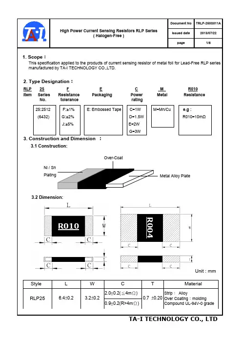
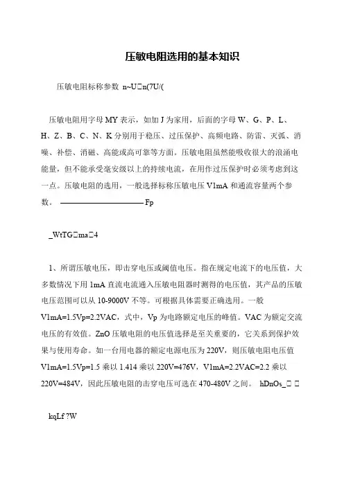
大毅4527大功率合金电阻RLP45系列选型手册
- 格式:pdf
- 大小:631.16 KB
- 文档页数:8
大品牌采样电阻,台产品牌合金电阻首页大毅代理光颉代理泰艺代理今台代理阿尔卑斯关于我们品牌合作联系我们大品牌采样电阻,台产品牌合金电阻大品牌采样电阻,台产品牌合金电阻 大毅科技成立於1986年,为全球第二大SMD厚膜晶片电阻制造供应商,在结合坚强的经营团队,以最先进的设 备与技术,制造高品质的零组件及最具竞争优势之价格与服务,在客户端奠定良好之信誉. 采样电阻基本参数: 产品型号 RLM12FTCMR020 电阻阻值 0.02Ω 电阻精度 1% 封装尺寸 1206 温度系数 50 额定功率1W 产品品牌 大毅 产品材质 合金 工作温度 -55~+125℃ 1206合金电阻相关尺寸图: 1206合金电阻功率曲线图: 功率随温度发生变化,温度越高功率越小。
1206合金电阻主要用于:电池保护板,适配器,电子烟控制板,电动工具,智能家居,通信设备,平衡车,定位模块 伺服电机,LED照明设备等产品。
本公司大量备货1206合金电阻,阻值1毫欧~50毫欧,欢迎来电咨询及查货,捷比信实业合金电阻优质供应商。
主要产品 厚膜晶片电阻、厚膜晶片排阻、低阻抗晶片电阻、薄膜晶片电阻、微阻抗金属电阻器、薄膜晶片保险丝。
电路中如何选择合适的电阻简析2016年云计算四大发展趋势张进华:充电桩数量不足不是最大阻碍晶振在VR产品中的应用泰艺TY系列2520封装TCXO 温补晶振频点最大可做52MHZ智能电动平衡车电路设计图台湾光颉LRP系列合金电阻温漂系数低至50ppm满足航空应用对电阻性能的新需求您现在的位置:首页 >毫欧电阻满足航空应用对电阻性能的新需求光颉0201*4贴片排阻军标级电阻 0.01%精密电阻 万分之一精度电阻 薄膜精密电阻精密电阻 合金电阻 大功率电阻 采样电阻 毫欧电阻 台湾大毅 台湾光颉 产品中心 联系方式 品牌合作 Kingbright代理 今台代理知识版权所有 Copyright © All RIGHTS RESERVED. 网站统计。
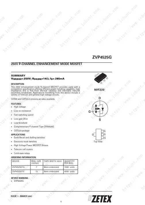
wcwowmh.titcphsu:n/t/.wcwowmh.titcphsu:n/t/.wcwowmh.titcphsu:n/t/.wcwowmh.titcphsu:n/t/.wcwowm.hitcthpusn:t/./cwowmwh.titcphsu:n/t/.wcwowmh.titcphsu:n/t/.wcwowmh.titcphsuZVP4525G250V P-CHANNEL ENHANCEMENT MODE MOSFETSUMMARY(m om c DESCRIPTION m o c . This 250V enhancement mode N-channel MOSFET provides users with a m om co .c t. nt competitive specification offering efficient power handling capability, high m o c . t n u impedance and is free from thermal runaway and thermally induced m o c . t n u h secondary breakdown. Applications benefiting from this device include a o c . t n u h c variety of Telecom and general high voltage circuits. t.c nt. unt hun chu ich .ic w.i SOT89 and SOT23-6 versions are also available. un hu ch ic .i w. ww ww /w FEATURES ch ic .i w. ww ww /w // :/ • High voltage i ww. www /ww //w :// s:/ ps: tps • Low on-resistance /w // :/ s: ps tp tt ht • Fast switching speed :/ s: ps tp tt ht h • Low gate drive ttps http htt ht h • Low thresholdSOT223• Complementary P-channel Type ZVN4525G• SOT223 packageAPPLICATIONS • Earth Recall and dialling switchesSDDG• Electronic hook switchesTop View• High Voltage Power MOSFET Drivers• Telecom call routers:n/t/.wcwowmh.IOD••StiDZZERSVVtcVEDUSZPPVIVEophEC44IRlPCEsui551d4IE22NM:n5-55sG2MtGGA/ta5RAITTtG/.NeACKRwcFrICNOewoHlGRawmy2Ms0h.A0tiT1(RiItcnEOcEphNhL1sue73Ss:nI)Z/tE/.wcT88wommAwmPmmEh.eeWtimmItcDbbphooTssHsussee:n(mdd/tm/.1)wcwoPQ41wm00EU00Rh.A00RNtiuuETtcnnEITphiiLttYsssu:n/t/.wcwowmh.titcphsu:n/t/.wcwowmh.titcphsu:n/t/.wcwowm.hitcthpusn:t/./cwowmwh.tiwcwowmh.titcphsu:n/t/.wcwowmh.titcphsu:n/t/.wcwowmh.titcphsu:n/t/.wcwowmh.titcphsu:n/t/.wcwowm.hitcthpusn:t/./cwowmwh.titcphsu:n/t/.wcwowmh.titcphsu:n/t/.wcwowmh.titcphsuZVP4525GABSOLUTE MAXIMUM RATINGS.PARAMETERSYMBOLLIMITUNITDrain-Source VoltageVDSS250VGate Source VoltageVGS±40VContinuous Drain Current (VGS=10V; TA=25°C)(a) ID-265mA(VGS=10V; TA=70°C)(a) ID-212mAPulsed Drain Current (c)m om c Continuous Source Current (Body Diode) m om co .c t. Pulsed Source Current (Body Diode) m om co .c t. nt un Power Dissipation at TA=25°C (a) m o c . t n u h Linear Derating Factor co .c t. nt un hu ch ic Operating and Storage Temperature RangeIDM IS ISM PD:Tj Tstg-1 -0.75-1 2 16 -55 to +150A A A W mW/°C °Cichun/t/.www.ichu:n/t/www.ichsu:n//www.icphsu://www.itcphs://www.titcps://wwwh.titps://www.https://w THERMAL RESISTANCE s: ps tp tt ht h PARAMETERttp htt ht h Junction to Ambient (a)SYMBOL RθJAVALUE 63UNIT °C/WJunction to Ambient (b)RθJA26°C/WNOTES(a) For a device surface mounted on 25mm x 25mm FR4 PCB with high coverage of single sided 1oz copper, in still air conditions(b) For a device surface mounted on FR4 PCB measured at tр5 secs.(c) Repetitive rating - pulse width limited by maximum junction temperature. Refer to Transient Thermal Impedance graph.:n/t/.wcwowmh.NFvtiooBrltctHahphgiiggesuhhs:nVvpoa/tolclt/.tiaangwcggeewobaAewmptpwph.pleilticiecatcnattiphcoioonsunnss:nd, tu/thce/.toawcrpswo.prwmoph.rtiiattcephinsud:nus/ttr/.y2wcsewoctwmorh.gtiutcidphelsuin:nes/ts/.howcuwoldwmbh.eticotcnISphsiSsudUe:nrEe/t1d/.-wwcMitwoAhRwmreCh.gHatir2dtc00tpho1su:n/t/.wcwowm.hitcthpusn:t/./cwowmwh.tiwcwowmh.titcphsu:n/t/.wcwowmh.titcphsu:n/t/.wcwowmh.titcphsu:n/t/.wcwowmh.titcphsu:n/t/.wcwowm.hitcthpusn:t/./cwowmwh.titcphsu:n/t/.wcwowmh.titcphsu:n/t/.wcwowmh.titcphsuCHARACTERISTICSZVP4525Gtitcphsu:n/t/.wcwowmh.titcphsu:n/t/.wcwowmh.titcphsu:n/t/.wcwowmh.titcphsu:n/t/.wcwowmh.titcphsu:n/t/.wcwowmh.titcphsu:n/t/.wcwowmh.titcphsu:n/t/.wcwowm.hitcthpusn:t/./cw:n/t/.wcwowmh.IStiStcUphEsu1 :n- M/tA/.RwcCwoHwm20h.0ti1tcphsu:n/t/.wcwowmh.titcphsu:n/t/.3wcwowmh.titcphsu:n/t/.wcwowmh.titcphsu:n/t/.wcwowmh.titcphsu:n/t/.wcwowm.hitcthpusn:t/./cwowmwh.tiwcwowmh.titcphsu:n/t/.wcwowmh.titcphsu:n/t/.wcwowmh.titcphsu:n/t/.wcwowmh.titcphsu:n/t/.wcwowm.hitcthpusn:t/./cwowmwh.titcphsu:n/t/.wcwowmh.titcphsu:n/t/.wcwowmh.titcphsuZVP4525GELECTRICAL CHARACTERISTICS (at Tamb = 25°C unless otherwise stated).PARAMETERSYMBOL MIN. TYP. MAX. UNIT CONDITIONS.STATICDrain-Source Breakdown VoltageV(BR)DSS -250-285VID=-1mA, VGS=0VZero Gate Voltage Drain CurrentIDSSm om c Gate-Body LeakageIGSSm om co .c t. Gate-Source Threshold VoltageVGS(th)-0.8m om co .c t. nt un Static Drain-Source On-State Resistance (1) RDS(on)com .co t.c nt. unt hun chu ich Forward Transconductance (3) nt. unt hun chu ich .ic w.i ww. w DYNAMIC (3) hu ch ic .i w. ww ww /w // Input Capacitance ic .i w. ww ww /w // :/ s: Output Capacitanceww ww /w // :/ s: ps tp Reverse Transfer Capacitance /w // :/ s: ps tp tt ht SWITCHING(2) (3) s:/ ps: tps ttp htt ht h Turn-On Delay Time ttp htt ht h Rise Timegfs80Ciss Coss Crsstd(on) tr-30-500 nA VDS=-250V, VGS=0V±1±100 nA VGS=±40V, VDS=0V-1.5 -2.0 VI =-1mA,DVDS=VGS1014ΩVGS=-10V, ID=-200mA1318ΩVGS=-3.5V, ID=-100mA200mS VDS=-10V,ID=-0.15A73 12.8 3.91pF VDS=-25 V, VGS=0V,pF f=1MHzpF1.53 3.78nsVDD =-30V, ID=-200mA ns RG=50Ω, VGS=-10V(refer to test circuit)Turn-Off Delay Timetd(off)17.5nsFall Timetf7.85nsTotal Gate Charge Gate-Source Charge Gate Drain ChargeQg2.45 3.45 nCVDS=-25V,VGS=-10V,Qgs0.22 0.31 nC ID=-200mA(refer totest circuit)Qgd0.45 0.63 nCSOURCE-DRAIN DIODEDiode Forward Voltage (1)VSD0.97 VTj=25°C, IS=-200mA,VGS=0Vm Reverse Recovery Time (3)trrm om co Reverse Recovery Charge (3)Qrr205290 ns Tj=25°C, IF=-200mA,di/dt= 100A/µs2129nCm om com .co t.c nt. (1) Measured under pulsed conditions. Width=300µs. Duty cycle ≤2% . m o c . t n u (2) Switching characteristics are independent of operating junction temperature. m o c . t n u h (3) For design aid only, not subject to production testing.:n/t/.wcwow.icphsu:n/t/.wcww.itcphsu:n/t/.www.titcphsu:n/t/wwwh.titcphsu:n//wwwh.titcphsu://wwwh.titcphs://www.hitctps://wwwh.ti ISSUE 1 - MARCH 2001 htt ht h 4wcwowmh.titcphsu:n/t/.wcwowmh.titcphsu:n/t/.wcwowmh.titcphsu:n/t/.wcwowmh.titcphsu:n/t/.wcwowm.hitcthpusn:t/./cwowmwh.titcphsu:n/t/.wcwowmh.titcphsu:n/t/.wcwowmh.titcphsuTYPICAL CHARACTERISTICSZVP4525Gtitcphsu:n/t/.wcwowmh.titcphsu:n/t/.wcwowmh.titcphsu:n/t/.wcwowmh.titcphsu:n/t/.wcwowmh.titcphsu:n/t/.wcwowmh.titcphsu:n/t/.wcwowmh.titcphsu:n/t/.wcwowm.hitcthpusn:t/./cw:n/t/.wcwowmh.IStiStcUphEsu1 :n- M/tA/.RwcCwoHwm20h.0ti1tcphsu:n/t/.wcwowmh.titcphsu:n/t/.5wcwowmh.titcphsu:n/t/.wcwowmh.titcphsu:n/t/.wcwowmh.titcphsu:n/t/.wcwowm.hitcthpusn:t/./cwowmwh.tiZVP4525GCHARACTERISTICSISSUE 1 - MARCH 2001 6TEST CIRCUITSZVP4525GISSUE 1 - MARCH 2001 7ZVP4525GPACKAGE DIMENSIONSPAD LAYOUT DETAILS4.62.0 min (3x)2.31.5 min(3x)6.82.0 min 3.8 minDimMillimetersMinMaxA6.36.7B3.33.7C–1.7D0.60.8E2.93.1F0.240.32GNOM 4.6H0.851.05K0.020.10L6.77.3MNOM 2.3InchesMinMax0.2480.2640.1300.146–0.0670.0240.0310.1140.1220.0090.013NOM 0.1810.0330.0410.00080.0040.2640.287NOM 0.0905Zetex GmbH Streitfeldstraße 19 D-81673 München Germany Telefon: (49) 89 45 49 49 0 Fax: (49) 89 45 49 49 49Zetex plc. Fields New Road, Chadderton, Oldham, OL9-8NP, United Kingdom. Telephone: (44)161 622 4422 (Sales), (44)161 622 4444 (General Enquiries) Fax: (44)161 622 4420Zetex Inc. 47 Mall Drive, Unit 4 Commack NY 11725 USA Telephone: (631) 543-7100 Fax: (631) 864-7630Zetex (Asia) Ltd. 3701-04 Metroplaza, Tower 1 Hing Fong Road, Kwai Fong, Hong Kong Telephone:(852) 26100 611 Fax: (852) 24250 494These are supported by agents and distributors in major countries world-wide © Zetex plc 2000Ths publication is issued to provide outline information only which (unless agreed by the Company in writing) may not be used, applied or reproduced for any purpose or form part of any order or contract or be regarded as a representation relating to the products or services concerned. The Company reserves the right to alter without notice the specification, design, price or conditions of supply of any product or service.ISSUE 1 - MARCH 20018。
大毅合金电阻
一、简介
大毅合金电阻是一种精密度高、稳定性好的电阻产品。
它主要由合金线材、PVC外壳、阻值等组成,具有良好的电性能,特别是频率响应,具有良好的阻燃特性,耐高温、耐湿、耐高压的性能。
此外,它也具有运行稳定、耐久性能、精度高、结构紧凑、体积小、重量轻等优点。
二、性能
1、高精度:大毅合金电阻具有较高的电压精度,即最大允许误差。
2、稳定性:它具有较高的温度稳定性,即温度变化不会引起其阻值变化,而且运行可靠性高。
3、耐久性:大毅合金电阻具有良好的耐久性,有耐高温、耐湿、耐高压的性能。
4、耐腐蚀性:大毅合金电阻具有良好的耐腐蚀性,可有效耐受各种有毒气体和环境污染,能够长期稳定使用。
三、应用
大毅合金电阻有着良好的性能,所以它的应用非常广泛,主要用于电源供电、电机驱动、控制电路、信号放大器等设备上,广泛用于家用电器、专业仪器、科学仪器、自动化设备等。
- 1 -。
2017/2/8大毅4527贴片合金采样电阻常备料型号查询表【捷比信科技】/info/20141524.html 1/10624系列一体成型电感 移动电源专用模压电感苹果收购不为进军晶圆业 原厂或成MEMS 研发中心圆柱状精密电阻光颉通过AECQ200薄膜车规电阻华为离开的背后:深圳,你是要房地产还是要制造业给大脑植入芯片不是梦,硅谷已经行动了2016无人机送快递扎堆 韩拟今年实现无人机配送快递动力电池技术是在争辩中变化,发展的人机交互新突破:手臂变成触摸板浅谈待机能耗问题及其电源解决方案首页 > 行业资讯 > 大毅4527贴片合金采样电阻常备料型号查询表大毅4527贴片合金采样电阻常备料型号查询表捷比信科技整理的大毅4527贴片合金采样电阻常备料型整理如下: RLP45FEJR006 RLP45FEJR007 RLP45FEJR008 RLP45FEJR009RLP45FEJR010 RLP45FEJR012 RLP45FEJR015 RLP45FEJR016 RLP45FEJR018 RLP45FEJR020 RLP45FEJR022 RLP45FEJR025RLP45FEJR030 RLP45FEJR033 RLP45FEJR040 RLP45FEJR050.. 查货,索样请来电洽询大毅授权代理深圳市捷比信科技有限公司C: BY:陆 TIME:20170207随机推荐:知识版权所有 © 深圳市捷比信科技有限公司服务热线:+8675529796190 传真:+8675529796149 地址:深圳市龙华新区东环一路皇嘉中心A 座820822 Email :sales@电阻产品: 低温漂电阻 大毅电阻 Viking 光颉电阻 高精密低温漂电阻 采样电阻 大功率无感电阻 插件精密电阻 高频电感 汽车专用电阻 贴片保险丝 低温漂精密电阻 毫欧电阻 排阻泰艺晶振产品: 有源晶振 晶振封装 晶振频率 晶振精度 32.768K 晶振 恒温晶振 高温晶振 可编程晶振 温补晶振 压控晶振 无源晶振 贴片晶振 插件晶振 钟振 石英振荡器 晶振波形输出 SCcut 切晶振ALPS 代理产品: ALPS 编码器 ALPS 电位器 ALPS 开关按键 ALPS 卡座连接器 ALPS TACT Switch网站统计走进捷比信大毅(TA-I)光颉(Viking)阿尔卑斯(ALPS)公司简介资讯信息联系我们。