DM2307场效应管SOT-23厂家DCY品牌推荐
- 格式:pdf
- 大小:390.33 KB
- 文档页数:3

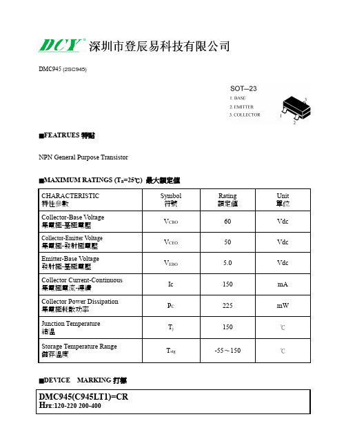
DMC945(C945LT1)=CR DMC945■FEATRUES 特點NPN General Purpose Transistor■MAXIMUMRATINGS (T a =25℃)最大額定值CHARACTERISTIC 特性參數Symbol 符號Rating 額定值Unit 單位Collector-Base V oltage 集電極-基極電壓V CBO 60Vdc Collector-Emitter Voltage集電極-發射極電壓V CEO 50Vdc Emitter-Base Voltage 發射極-基極電壓V EBO 5.0Vdc Collector Current-Continuous 集電極電流-連續Ic 150mA Collector Power Dissipation 集電極耗散功率P C 225mWJunction Temperature 結溫T j 150℃Storage Temperature Range 儲存溫度T stg-55〜150℃■DEVICE MARKING 打標H FE :120-220200-400(2SC945)■ELECTRICAL CHARACTERISTICS電特性(T A=25℃unless otherwise noted如無特殊說明,溫度爲25℃)Characteristic 特性參數Symbol符號Test Condition測試條件Min最小值Typ典型值Max最大值Unit單位Collector Cutoff Current 集電極截止電流I CBOV CB=60V,I E=0——0.1μAEmitter Cutoff Current 發射極截止電流I EBOV EB=5V,I C=0——0.1μACollector-Base Breakdown Voltage集電極-基極擊穿電壓V(BR)CBO I C=100μA60——VCollector-Emitter Breakdown Voltage集電極-發射極擊穿電壓V(BR)CEO I C=1.0mA50——VEmitter-Base Breakdown Voltage發射極-基極擊穿電壓V(BR)EBO I E=100μA5——VDC Current Gain 直流電流增益H FEV CE=6V,I C=1mA120—400—Collector-Emitter Saturation Voltage 集電極-發射極飽和壓降V CE(sat)I C=100mA,I B=10mA——0.3VBase-Emitter Saturation Voltage 基極-發射極飽和壓降V BE(sat)I C=100mA,I B=10mA—— 1.0VBase-Emitter Saturation 基極-發射極電壓V BEV CE=5.0V,I C=10mA——0.8VTransition Frequency 特徵頻率f TV CE=6.0V,I C=1mA—250—MHz DMC945(2SC945)。

Vishay SiliconixSi2307CDSP-Channel 30-V (D-S) MOSFETFEATURES•Halogen-free Option Available •TrenchFET ® Power MOSFETAPPLICATIONS•Load Switch for Portable DevicesPRODUCT SUMMARYV DS (V)R DS(on) (Ω)I D (A)a, b Q g (Typ.)- 300.088 at V GS = - 10 V - 2.7 4.1 nC0.138 at V GS = - 4.5 V- 2.2Notes:a. Surface Mounted on 1" x 1" FR4 board.b. t = 5 s.c. Maximum under Steady State conditions is 166 °C/W. ABSOLUTE MAXIMUM RATINGS T A = 25 °C, unless otherwise notedParameter Symbol Limit nitDrain-Source Voltage V DS - 30VGate-Source VoltageV GS± 20Continuous Drain Current (T J = 150 °C)a, bT C = 25 °CI D - 3.5A T C = 70 °C - 2.8T A = 25 °C - 2.7a, b T A = 70 °C- 2.2a, b Pulsed Drain Current (10 µs Pulse Width)I DM - 12Continuous Source-Drain Diode Current a, bT C = 25 °C I S - 1.5T A = 25 °C - 0.91a, bMaximum Power Dissipation a, bT C = 25 °CP D 1.8W T C = 70 °C 1.14T A = 25 °C 1.1a, b T A = 70 °C0.7a, b Operating Junction and Storage T emperature Range T J , T stg - 55 to 150°C Soldering Recommendations (Peak Temperature)c260THERMAL RESISTANCE RATINGSParameter Symbol Typical Maximum UnitMaximum Junction-to-Ambient a, c t ≤ 5 s R thJA 90115°C/WMaximum Junction-to-Foot (Drain)Steady StateR thJF5570Vishay SiliconixSi2307CDSNotes:a. Pulse test; pulse width ≤ 300 µs, duty cycle ≤ 2 %.b. Guaranteed by design, not subject to production testing.Stresses beyond those listed under “Absolute Maximum Ratings” may cause permanent damage to the device. These are stress ratings only, and functional operation of the device at these or any other conditions beyond those indicated in the operational sections of the specifications is not implied. Exposure to absolute maximum rating conditions for extended periods may affect device reliability.SPECIFICATIONS T J = 25 °C, unless otherwise notedParameter Symbol Test Conditions Min.Typ.Max.U nitStaticDrain-Source Breakdown Voltage V DS V GS = 0 V , I D = - 250 µA- 30V V DS Temperature Coefficient ΔV DS /T J I D = - 250 µA - 32mV/°C V GS(th) Temperature Coefficient ΔV GS(th)/T J 4.5Gate-Source Threshold Voltage V GS(th) V DS = V GS , I D = - 250 µA - 1- 3VGate-Source LeakageI GSS V DS = 0 V , V GS = ± 20 V - 100nAZero Gate Voltage Drain Current I DSS V DS = - 30 V , V GS = 0 V - 1µA V DS = - 30 V , V GS = 0 V , T J = 55 °C- 10On-State Drain Current aI D(on) V DS ≤ 5 V , V GS = - 10 V - 6A Drain-Source On-State Resistance a R DS(on) V GS = - 10 V , I D = - 3.5 A 0.0730.088ΩV GS = - 4.5 V , I D = - 2.5 A 0.1100.138Forward T ransconductance a g fsV DS = - 10 V, I D = - 3.5 A7SDynamic bInput Capacitance C iss V DS = - 15 V , V GS = 0 V, f = 1 MHz340pFOutput CapacitanceC oss 67Reverse Transfer Capacitance C rss 51Total Gate Charge Q g V DS = - 15 V , V GS = - 4.5 V , ID = - 2.5 A 4.1 6.2nC Gate-Source Charge Q gs 1.3Gate-Drain Charge Q gd 1.8Gate Resistance R g f = 1 MHz10ΩTurn-On Delay Time t d(on) V DD = - 15 V, R L = 15 Ω I D ≅ - 1 A, V GEN = - 4.5 V , R g = 1 Ω4060nsRise Timet r 4060Turn-Off Delay Time t d(off) 2040Fall Timet f 1730Turn-On Delay Time t d(on) V DD = - 15 V, R L = 15 ΩI D ≅ - 1 A, V GEN = - 10 V, R g = 1 Ω 5.510Rise Timet r 1325Turn-Off Delay Time t d(off) 1730Fall Timet f7.715Drain-Source Body Diode Characteristics Continuous Source-Drain Diode Current I S T C = 25 °C- 1.5A Pulse Diode Forward Current I SM - 12Body Diode VoltageV SD I S = - 0.75 A, V GS = 0 V- 0.8- 1.2V Body Diode Reverse Recovery Time t rr I F = - 2.5 A, dI/dt = 100 A/µs, T J = 25 °C1730ns Body Diode Reverse Recovery Charge Q rr 1120nC Reverse Recovery Fall Time t a 12nsReverse Recovery Rise Timet b5On-Resistance vs. Drain Current and Gate VoltageGate ChargeCapacitanceOn-Resistance vs. Junction TemperatureSource-Drain Diode Forward VoltageThreshold VoltageOn-Resistance vs. Gate-to-Source VoltageSingle Pulse Power, Junction-to-AmbientVishay SiliconixSi2307CDSTYPICAL CHARACTERISTICS 25°C, unless otherwise notedVishay Silico nix maintains wo rldwide manufacturing capability. Pro ducts may be manufactured at o ne o f several qualified lo catio ns. Reliability data fo r Silico n Technology and Package Reliability represent a composite of all qualified locations. For related documents such as package/tape drawings, part marking, and reliability data, see /ppg?68768.Disclaimer Legal Disclaimer NoticeVishayAll product specifications and data are subject to change without notice.Vishay Intertechnology, Inc., its affiliates, agents, and employees, and all persons acting on its or their behalf (collectively, “Vishay”), disclaim any and all liability for any errors, inaccuracies or incompleteness contained herein or in any other disclosure relating to any product.Vishay disclaims any and all liability arising out of the use or application of any product described herein or of any information provided herein to the maximum extent permitted by law. The product specifications do not expand or otherwise modify Vishay’s terms and conditions of purchase, including but not limited to the warranty expressed therein, which apply to these products.No license, express or implied, by estoppel or otherwise, to any intellectual property rights is granted by this document or by any conduct of Vishay.The products shown herein are not designed for use in medical, life-saving, or life-sustaining applications unless otherwise expressly indicated. Customers using or selling Vishay products not expressly indicated for use in such applications do so entirely at their own risk and agree to fully indemnify Vishay for any damages arising or resulting from such use or sale. Please contact authorized Vishay personnel to obtain written terms and conditions regarding products designed for such applications.Product names and markings noted herein may be trademarks of their respective owners.元器件交易网。