RT9202主板DRR内存供电控制芯片
- 格式:doc
- 大小:287.50 KB
- 文档页数:3
RT8802A的针脚封装图11规范,最低电压步进为6.25mV。
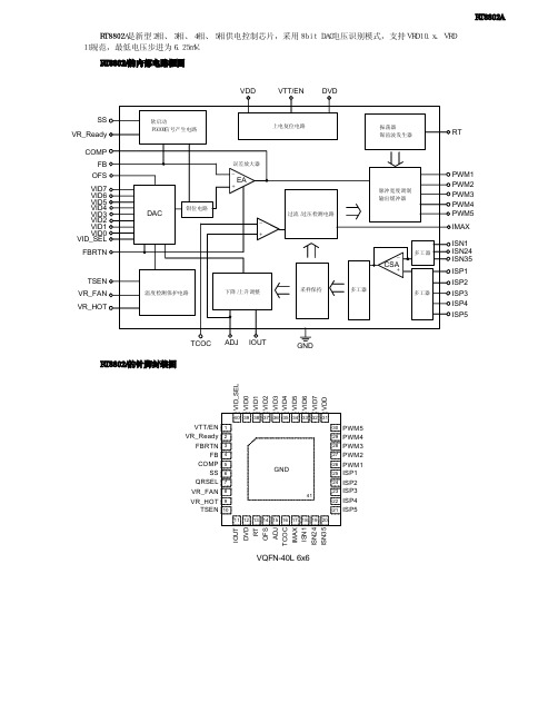
RT8802A是新型2相、3相、4相、5相供电控制芯片,采用8bit DAC电压识别模式,支持VRD10.x、VRD RT8802RT8802A RT8802A的内部电路框图VQFN-40L 6x6VTT/EN VR_ReadyFBRTNFB COMPSS QRSEL VR_FAN VR_HOT TSENI O U TD V DR T O F SA D J T C O CI M A X I S N 1I S N 24I S N 35I D _S E LI D 0I D 1I D 2I D 3I D 4I D 5I D 6I D 7D D引脚号引脚名称引脚功能1VTT/EN 使能控制端2VR_Ready Power Good 信号输出端3FBRTN 反馈接地端4FB 输出电压反馈电压信号输入端5COMP 误差放大器输出端6SS 软启动控制器7QRSEL 快速响应模式设置端8VR_FAN 超温报警信号输出端,开漏极输出9VR_HOT 过热报警信号输出端10TSEN 过热温度检测输入端11IOUT 输出电流设置端12DVD 12V 电压过压检测输入端13RT 振荡器频率设置端14OFS 负载悬空设置端15ADJ 输出电流设置端16TCOC 过流检测设置端17IMAX 过流保护启动电流设置端18ISN1电流反馈端119ISN24电流反馈端220ISN35电流反馈端321ISP5过流检测端22ISP4过流检测端23ISP3过流检测端24ISP2过流检测端25ISP1过流检测端26PWM1PWM 信号输出端127PWM2PWM 信号输出端228PWM3PWM 信号输出端329PWM4PWM 信号输出端430PWM5PWM 信号输出端531VDD 5V 供电电压输入端32VID7电压工作模式设置端33VID6CPU 电脑模式识别端。
若这7个引脚均悬空,则工作在“无CPU ”模式,此时无控制信号输出。
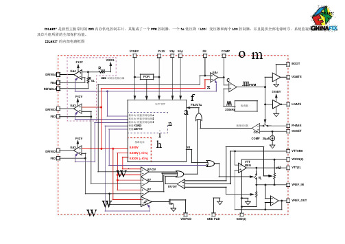
ISL6537ISL6537是新型主板常用的DDR内存供电控制芯片,其集成了一个PWM控制器、一个3A低压降(LDO)变压器和两个LDO控制器,并且提供全部电源时序、系统监视和DDR及芯片组所需的全部保护功能。
ISL6537的内部电路框图m5VSBY P12V S3# S5# FB COMP oP12VVDDQEA4 RGUEA1DRIVE4POR .R GL GMCH 双低压差稳压器 cFB4PWMxREFADJ45VSBY P12V fEA3 监控电路FAULT i 振荡器250kHzDRIVE3 aFB3 软启动/使能控制电路A软启动/使能控制电路B软启动/使能控制电路C n使能VIDPGD 振荡比较器使能DDR-VTTi OCP12V COMP 20µA基准电压hEA2 0.800V S3DRIVE2 0.680V (-15%)cFB2 0.920V (+15%)VTT.UV/OV REGR UwUVR LUVUV/OVwwVIDPGD GND PAD GND(2) BOOT UGATELGATEPHASE OCSETVTTSNS VDDQ(2) VTT(2)VREF_IN VREF_OUTISL6537的针脚封装图L G A T EG N DU G A T EB O O TP H A S ES 5#O C S E T28 27 26 25 24 23 225VSBY 121 DRIVE4S3# 2P12V 3 GND 4DDR_VTT 5 DDR_VTT 6 VDDQ7ISL6537的各引脚功能引脚号 引脚名称 1 5VSBY 2 S3# 3 P12V 4 GND5 VTT_DDR6 VTT_DDR7 VDDQ 8VDDQ9 VTTSNS_DDR10DRIVE2 c11FB212.VIDPGD13wOUT_VREF 14 wIN_VREF15FB16 COMP 17 FB418FB319DRIVE3w20REFADJ4 21DRIVE4 22 OCSET23S5# 24 PHASE 25BOOT26 UGATE27 PAD GND28LGATE20 REFADJ4GND19 DRIVE3FB3182917 FB416 COMP15 FBm8 9 10 11121314V D D QD D R V T T S N SD R I VE 2F B 2V I D P G DV R E F O U TV R E F I Nco.引脚功能待机供电电压输入端 +5Vi睡眠模式设定# S3/5_SLP x供电电压输入端 12V f 接地端 a无(睡眠模式下为禁用 S3 在,电压输出端 VTT 睡眠模式下为 S0/S1 在 )输出 n 书面模式下作为输入脚 S0/S1 在,电压检测输入端 VDDQi书面模式下作为输入脚 S0/S1 在,电压检测输入端 VDDQ h反馈电压输入端 VTT DDR驱动信号输出端 2 反馈端在;此信号为高电平,睡眠模式下 S0/S1/S2 信号输出端。

c202芯片组C202芯片组是英特尔(Intel)公司推出的一款服务器主板芯片组。
C202芯片组支持英特尔Xeon E3-1200处理器和第二代英特尔Core i3系列处理器,是专为单插槽服务器设计的。
它可以提供出色的性能和可靠性,适用于小型企业和办公室环境。
C202芯片组支持最多32GB DDR3-1333/1066ECC和非ECC内存,可通过ECC存储技术保护数据的完整性和可靠性。
它还支持Intel Flex Memory Access(弹性内存访问)技术,可以根据应用程序的需求自动调整内存带宽,提高服务器的性能和效率。
C202芯片组还具有强大的存储功能。
它支持SATA 6Gb/s和SATA 3Gb/s接口,可以连接多种硬盘和光驱设备。
它还支持RAID 0, 1, 5和10,可以提供额外的数据保护和性能提升。
此外,C202芯片组还支持USB 3.0和PCI Express 2.0接口,提供更快的数据传输速度和更高的扩展性。
C202芯片组还具有集成的英特尔HD图形技术,支持高清视频和图形处理。
它可以提供更好的视觉体验,适用于诸如数字广告、多媒体展示和视频会议等应用。
在安全性方面,C202芯片组支持英特尔管理引擎(Intel Management Engine)和英特尔服务器系统管理软件(Intel Server System Management Software)。
它可以提供远程管理和监控,确保服务器的安全和稳定运行。
总而言之,C202芯片组提供了出色的性能和可靠性,适用于小型企业和办公室环境。
它具有强大的存储功能、高清图形处理和远程管理等特点,为用户提供了一个完善的解决方案。
无论是运行企业应用程序还是提供多媒体服务,C202芯片组都能满足用户的需求。
DS9202-02 August DS9202-02 August Absolute Maximum Ratingsz Supply Voltage VCC 7Vz BOOT & UGATE to GND 15Vz Input, Output or I/O Voltage GND−0.3V ~ 7V z Power Dissipation, P D @ T A = 25°CSOP-80.625Wz Package Thermal ResistanceSOP-8, θJA160°C/Wz Ambient Temperature Range0°C ~ +70°Cz Junction Temperature Range-40°C ~ +125°C z Storage Temperature Range-65°C ~ +150°C z Lead Temperature (Soldering, 10 sec.)260°C CAUTION:Stresses beyond the ratings specified in “Absolute Maximum Ratings” may cause permanent damage to the device. This is a stress only rating and operation of the device at these or any other conditions above those indicated in the operational sections of this specification is not implied.Electrical Characteristics(V CC = 5V, T A = 25°C, Unless otherwise specified.)Parameter Symbol Test Conditions Min Typ Max Units VCC Supply Current / Regulated VoltageNominal Supply Current I CC UGATE, LGATE open--36mA Regulated Voltage from BOOT V CC V BOOT = 12V567V Power-On ResetRising VCC Threshold V OCSET = 4.5V 3.85 4.1 4.35V VCC Threshold Hysteresis V OCSET1 = 4.5V0.30.50.7V Rising V OCSET Threshold0.8 1.25 2.0V ReferenceReference Voltage0.7840.80.816V OscillatorFree Running Frequency250300350KHz Ramp Amplitude∆ V OSC-- 1.75--V P-P Error AmplifierDC gain323538dB PWM Controller Gate DriverUpper Drive Source R UGATE BOOT= 12VBOOT-V UGATE = 1V--711ΩUpper Drive Sink R UGATE V UGATE = 1V--57.5ΩLower Drive Source R LGATE VCC - V LGATE = 1V,--46ΩLower Drive Sink R LGATE V LGATE = 1V--24ΩTo be continuedDS9202-02 August DS9202-02 August Typical Operating CharateristicsTime UGATELGATE V CC = 5VDead TimeDead TimeTimeLGATEV CC = 5VUGATEPower OnTime V CCV CC = 5V V OUT = 2.2VV OUT Power OffTimeV CCV CC = 5V V OUT = 2.2VV OUTLoad TransientTime UGATEV CC = 5V V OUT = 2.2V C OUT = 3000µFV OUTLoad TransientTimeUGATEV CC = 5V V OUT = 2.2V C OUT = 3000µFV OUTShort HiccupV OUT V CC = 5VV OUT = 2.2VBootstrap Wave FormLGATE V CC = 5V; V OUT = 2.2VUGATEFunctional DescriptionThe RT9202 operates at either single 5V power supply with a bootstrap UGATE driver or 5V/12V dual-power supply form the ATX SMPS. The dual-power supply is recommended for high current application, the RT9202 can deliver higher gate driving current while operating with ATX SMPS based on dual-power supply.The Bootstrap OperationIn a single power supply system, the UGATE driver of RT9202 is powered by an external bootstrap circuit, as the Fig.1. The boot capacitor, C BOOT, generates a floating reference at the PHASE pin. Typically a0.1µF C BOOT is enough for most of MOSFETs used with the RT9202. The voltage drop between BOOT and PHASE is refreshed to a voltage of VCC – diode drop (V D) while the low side MOSFET turning on.Fig.1 Single 5V power Supply OperationDual Power OperationThe RT9202 was designed to regulate a 6.0V at VCC pin automatically when BOOT pin is powered by 12V. In a system with ATX 5V/12V power supply, the RT9202 is ideal for higher current application due to the higher gate driving capability, V UGATE = 7V and V LGATE = 6.0V. A RC (10Ω/1µF) filter is also recommended at BOOT pin to prevent the ringing induced from fast power on, as shown in Fig.2.Fig.2 Dual Power Supply OperationPower On ResetThe Power-On Reset (POR) monitors the supply voltage (normal +5V) at the VCC pin and the input voltage at the OCSET pin. The VCC POR level is 4.1V with 0.5V hysteresis and the normal level at OCSET pin is 1.5V (see over-current protection). The POR function initiates soft-start operation after all supply voltages exceed their POR thresholds.Soft StartA built-in soft-start is used to prevent surge current from power supply input during power on. The soft-start voltage is controlled by an internal digital counter. It clamps the ramping of reference voltage at the input of error amplifier and the pulse-width of the output driver slowly. The typical soft-start duration is 2mS.Over-Current ProtectionThe over current protection (OCP) function of the RT9202 is triggered when the voltage across the R DS(ON) of upper side MOSFET that developed by drain current exceeds over-current tripping level. An external resistor (R OCSET) programs the over-current tripping level of the PWM converter. As shown on Fig.1, the internal 40µA current sink (I OCSET) develops a voltage across R OCSET (V SET) that is referenced to V IN. The DRIVE signal enables the over-current comparator (OC). When the voltage across the upper MOSFET (V DS(ON)) exceeds V SET, the over-currentVCCDS9202-02 August DS9202-02 August Applications InformationInductor SelectionThe RT9202 was designed for V IN = 5V, step-down application mainly. Fig.5 shows the typical topology and waveforms of step-down converter.The ripple current of inductor can be calculated as follows:IL RIPPLE = (5V - V OUT )/L × T ON Because operation frequency is fixed at 300kHz,T ON = 3.33 × V OUT /5V The V OUT ripple isV OUT RIPPLE = IL RIPPLE × ESR ESR is output capacitor equivalent series resistor Table 1 shows the ripple voltage of V OUT : VIN = 5VTable 1Fig.5V OUT 3.3V2.5V1.5VInductor2µH 5µH 2µH5µH 2µH 5µH 1000µF (ESR=53m Ω)100mV 40mV 110mV 44mV 93mV37mV 1500µF (ESR=33m Ω)62mV 25mV 68mV 28mV 58mV 23mV 3000µF (ESR=21m Ω)40mV16mV43mV18mV37mV15mV*Refer to Sanyo low ESR series (CE, DX, PX…)The suggested L and C are as follows:2µH with ≥ 1500µF C OUT 5µH with ≥ 1000µF C OUTT ON T OFFV V -VI L = I Oi i I Qi I DC.C.M.V OVFig. 9PWM Layout ConsiderationsMOSFETs switch very fast and efficiently. The speed with which the current transitions from one device to another causes voltage spikes across the interconnecting impedances and parasitic circuit elements. The voltage spikes can degrade efficiency and radiate noise, that results in ocer-voltage stress on devices. Careful component placement layout and printed circuit design can minimize the voltage spikes induced in the converter. Consider, as an example, the turn-off transition of the upper MOSFET prior to turn-off, the upper MOSFET was carrying the full load current. During turn-off, current stops flowing in the upper MOSFET and is picked up by the low side MOSFET or Schottky diode. Any inductance in the switched current path generates a large voltage spike during the switching interval. Careful component selections, layout of the critical components, and use shorter and wider PCB traces help in minimizing the magnitude of voltage spikes.There are two sets of critical components in a DC-DC converter using the RT9202. The switching power components are most critical because they switch large amounts of energy, and as such, they tend to generate equally large amounts of noise. The critical small signal components are those connected to sensitive nodes or those supplying critical bypass current.The power components and the PWM controller should be placed firstly. Place the input capacitors,especially the high-frequency ceramic decoupling capacitors, close to the power switches. Place the output inductor and output capacitors between the MOSFETs and the load. Also locate the PWM controller near by MOSFETs.A multi-layer printed circuit board is recommended. Fig.10 shows the connections of the critical components in the converter. Note that the capacitors CIN and COUT each of them represents numerous physical capacitors. Use a dedicated grounding plane and use vias to ground all critical components to this layer. Apply another solid layer as a power plane and cut this plane into smaller islands of common voltage levels. The power plane should support the input power and output power nodes. Use copper filled polygons on the top and bottom circuit layers for the PHASE node, but it is not necessary to oversize this particular island. Since the PHASE node is subjected to very high dV/dt voltages, the stray capacitance formed between these island and the surrounding circuitry will tend to couple switching noise. Use the remaining printed circuit layers for small signal routing. The PCB traces between the PWM controller and the gate of MOSFET and also the traces connecting source of MOSFETs should be sized to carry 2A peak currents.Fig. 10DS9202-02 August DS9202-02 August RICHTEK TECHNOLOGY CORP. Headquarter5F, No. 20, Taiyuen Street, Chupei City Hsinchu, Taiwan, R.O.C.Tel: (8863)5526789 Fax: (8863)5526611RICHTEK TECHNOLOGY CORP. Taipei Office (Marketing)8F-1, No. 137, Lane 235, Paochiao Road, Hsintien City Taipei County, Taiwan, R.O.C.Tel: (8862)89191466 Fax: (8862)89191465Email: marketing@。

Dell PowerEdge R820机架式服务器是一款计算密集型高性能平台,提供高度可扩展内存(最高可配1.5 TB )和与之相匹配的强大I/O 功能,能够轻松运行大中型企业中的各种应用程序和虚拟化环境。
R820采用四个英特尔®至强® E5处理器,支持双RAID 控制器,可以轻松处理要求极为苛刻的任务关键型工作负载,如企业资源规划(ERP)、数据仓库、电子商务、虚拟桌面基础架构(VDI)、数据库和数据节点高性能计算(HPC)。
管理数据过载借助R820灵活而又强大的I/O 和存储功能,跟上虚拟化时代数据爆炸性增长的步伐。
多达16个内置硬盘和支持PCIe 3.0的集成扩展插槽可极大提高容量,而可选配的热插拔、正面接插PCIe 固态硬盘(最多4个)可实现性能增强和机箱内存储分层。
此外,戴尔精选网络适配器(我们灵活的网卡技术)让您能够视需要选择适宜的网络结构,无需占用宝贵的PCIe 插槽。
加速实施解决方案通过将PowerEdge R820的内存密度与可选的图形处理单元(GPU)加速器相结合,可以提高HPC 或2DVDI 环境的性能。
您可以从一系列GPU 选项中进行选择,以获得更大的辅助性能。
借助R820提高虚拟化水平PowerEdge R820可在四处理器配置中提供较大的内存容量、多种I/O 选项、灵活的结构选择和最多32个内核,有助于扩展您的虚拟环境,最大限度提高数据中心的应用程序容量。
选择业界领先的虚拟机管理程序,即可利用我们的系统管理功能来管理物理和虚拟资产。
R820还可以帮助您使用内置双SD 模块上的冗余故障保护型虚拟机管理程序,最大限度延长虚拟机的正常运行时间。
最后,通过戴尔的虚拟集成系统™ (VIS)解决方案,您只需轻点几下鼠标便可启用复杂的虚拟化环境。
PowerEdge 服务器系列PowerEdge 系列的各项功能与性能扩展能力完美组合,能够帮助各种规模的数据中心环境处理极具挑战性的工作负载。
[维修经验]简析RT9202与RT9214[复制链接]本帖最后由孤帆远影于 2009-12-6 21:23 编辑关于RT9202和RT9214的代换问题,很多帖子都已讨论过。
今天细看了这两个芯片的PDF。
现就这两种芯片的异同,简析如下:一,供电电压不同.RT9202工作电压为5V ,RT9214工作电压为5V或12V二,第七脚不完全相同虽同为过电流设置端(OCSET)。
且该脚被拉低到地时,都会关闭芯片的输出。
但是接法不相同RT9202 是在上管漏极和第七脚OCSET 脚之间接一电阻,来设定过电流保护的动作点。
RT9214是在其PHAST端和第七脚OPS之间接一电阻,来设定过电流保护的动作点为什么有的朋友会说这两种芯片能相互代换;有的会说9214能代换9202,反之就不行呢? 其实都没有说错假如一些板子上用的是9214或9202,但是没有用到他的第七脚的过流保护功能。
只是随便将该脚经过一个电阻上拉,然后接一个三极管(场管)的C极(漏极)。
该三极管(场管)的基极(G极),基于上电时序的需要,受控于桥。
如果再恰巧是5V 的VCC。
在这样的设计里,9214和9202就可以互换。
如果板子上用的是9214,VCC采用的是12V。
那换9202上去肯定不行。
如果板子上用的是9202,且9202第七脚的过电流保护功能通过外部元件启用了,那么理论上是不能用9214来代换的。
[主板]简析RT9202与RT9214[复制链接]楼主发表于 2009-12-7 19:00 |只看该作者|倒序浏览|打印关于RT9202和RT9214的代换问题,很多帖子都已讨论过。
今天细看了这两个芯片的PDF。
现就这两种芯片的异同,简析如下:一,供电电压不同.RT9202工作电压为5V ,RT9214工作电压为5V或12V二,第七脚不完全相同虽同为过电流设置端(OCSET)。
且该脚被拉低到地时,都会关闭芯片的输出。
但是接法不相同RT9202 是在上管漏极和第七脚OCSET 脚之间接一电阻,来设定过电流保护的动作点。
rts5420 用法-回复rts5420 用法:了解、配置和优化RTS5420是一种高性能和高度可定制的通用存储控制器芯片,用于固态硬盘(SSD)以及其他嵌入式存储设备。
其灵活的设计使其成为各种应用场景中的理想选择,从消费电子产品到数据中心和工业自动化系统。
本文将一步一步回答有关rts5420的用法问题,从了解该芯片开始,然后介绍如何配置和优化它以获得最佳性能。
第一步:了解RTS5420在使用RTS5420之前,了解其功能和特性是非常重要的。
RTS5420具有多个优势,例如高速数据传输、低功耗和丰富的接口选项等。
此外,它还支持多种存储器类型,包括NAND闪存、SD和eMMC卡等。
我们还需要了解rts5420的架构和工作原理。
其中包括控制器、内存和数据总线等关键组件。
此外,rts5420还提供了多种性能优化功能,例如强大的错误检测和纠正(ECC)机制、TRIM命令支持和高级缓存算法,以减少存储设备的读写延迟。
第二步:配置RTS5420配置RTS5420需要一些基本知识和技能。
首先,我们需要选择适当的接口,例如SATA、PCIe或USB,以与主机设备进行通信。
然后,我们需要根据存储设备的需求设置rts5420的工作模式和参数,例如传输速率、寻道时间和缓冲区大小等。
此外,rts5420还支持多种高级配置选项,例如TRIM命令和AHCI模式。
TRIM命令可用于通知SSD擦除无效的数据块,以提高闪存寿命和性能。
AHCI模式能够提供更高的数据传输速率和更好的兼容性,适用于较新的操作系统和主机设备。
第三步:优化RTS5420性能为了获得最佳性能,我们需要优化rts5420的配置和操作方式。
例如,我们可以通过调整读写缓存大小、启用写入加速和关闭非必要的功能来提高数据传输速率。
此外,我们还可以使用RTS5420提供的性能监控工具,例如传输速率和延迟的监视器,以了解和优化存储设备的性能。
除了配置rts5420本身,我们还可以优化主机系统和操作系统以提供更好的整体性能。
HPSSDEX920M.2 评测容量越大性价比越高
通过观察近年的SSD 市场的变化,我们可以发现M.2 接口SSD 早已普及市场了,这个趋势早已成为过去,而现在正在进行着的市场趋势就是从M.2 SATA3 协议转向M.2 NVMe 协议。
消费级NVMe SSD 的逐渐流行让众多的SSD 厂商也开始加入其中,惠普作为PC 领域的一大品牌,也开始从M.2 SATA3 SSD 转向了M.2 NVMe SSD。
而作为NVMe SSD 的排头兵就是HP SSD EX920 M.2。
HP SSD EX920 M.2 开箱与拆解
包装盒正面
包装盒背面
包装盒为黑底白字,标有产品型号、容量、PCI-e 和NVMe 标志,与HP
S700 的白色包装盒相比,纯黑的配色显示更加高端。
背面带有多个地区的免
责声明以及各种认证标志。
打开内部就能够看到HP SSD EX920 M.2 的本体了,配件有一个固定螺丝和作为背景板的说明书。
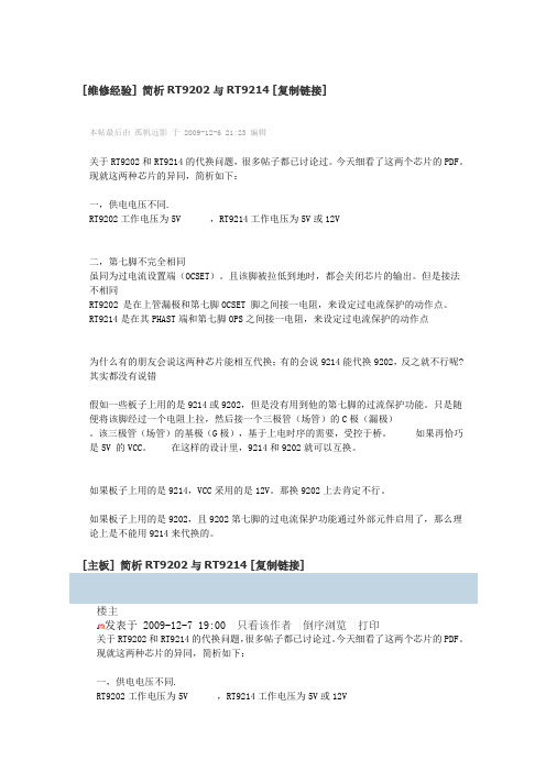
RT9202主板DRR内存供电控制芯片RT9202RT9202是RichTek 公司生产的双路同步降压线性PWM 控制芯片,在主板中通常用来作为DDR 内存供电控制芯片。
RT9202的内部电路框图VCC6.0VBOOT基准偏置上电复位0.8V40 A1V软启动m基准电压源+OCSETOC _o_OVPUGATE+c0.5V_UVP .PHASE+逻辑控制器 0.8V 35dB +xErrorFB+VCC_ 误差放大器PWM_iLGATEfGND300kHza振荡器iRT9202的针脚封装图nhPHASEBOOT18UGATE 27 OCSETcFB.GND 3 6LGATE45 VCCwRT9202各引脚功能w引脚号引脚名称引脚功能1wBOOT自举端2 UGATE上开关管驱动信号输出端 3 GND 接地端4 LGATE 下开关管驱动信号输出端5 VCC 供电电压输入端 6FB 电压反馈输入端7 OCSET 振荡频率设置端8 PHASE 过流检测反相输入端RT9202的典型应用电路图R15V20KR4108 PHASE BOOT 1C2MA732720.1∝FOCSET UGATE V OUTL2MUC5 +C1Q2RT9202 SHDN 632.5V1∝F470∝F2N7002H: shutdown FB GND5∝Hm54+C3VCC LGATE 1000∝F oC4R3R21∝Fc120 255C610nF .xifnaic hw.ww。