【集成电路(IC)】电子专业术语英汉对照加注解
- 格式:doc
- 大小:41.00 KB
- 文档页数:4
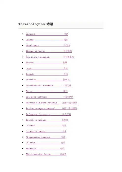
Terminologies 术语∙Circuit,电路∙Linear,线性∙Non-linear,非线性∙Planar circuit,平面电路∙Non-planar circuit,非平面电路∙Source,电源∙Load,负载∙Switch,开关∙Terminal,接线端∙Two-terminal elements,二端元件∙Port,端口∙One-port network,一端口网络∙Passive one-port network,无源一端口网络∙Active one-port network,有源一端口网络∙Reference direction,参考方向∙Branch variables,支路量∙Current,电流∙Direct current,直流∙Alternating current,交流∙Voltage,电压∙Potential,电位∙Electromotive force,电动势∙Associated reference directions,关联参考方向∙Non-associated reference directions,非关联参考方向∙power,功率∙resistors,电阻∙Ohm's law,欧姆定律∙Open circuit,开路∙Short circuit,短路∙independent sources,独立源∙dependent elements,受控元件∙dependent resources,受控源∙Active sign convention,有源符号约定∙Passive sign convention,无源符号约定∙branch,支路∙node,节点∙path,路径∙loop,回路∙mesh,网格∙serial connection,串联∙parallel connection,并联∙bridge,电桥∙balanced bridge,平衡电桥∙Y network,星型网络∙Δ network,三角形网络∙T network, T型网络∙π network,π型网络∙resistance match,电阻匹配∙Op Amp elements,运算放大器∙input resistance,输入电阻∙output resistance,输出电阻∙feedback,反馈∙ideal Op Amp,理想运放∙analog system,模拟系统∙digital system,数字系统∙noise,噪声∙buffer,缓冲器∙inverter,反相器∙AND,与门∙NAND,与非门∙OR,或门∙NOR,或非门∙true-value table,真值表∙logic expression,逻辑表达式∙MOSFET,(Metal-Oxide-Semiconductor Field-Effect Transistor)氧半场效晶体管∙two-port,二端口∙G parameter, G参数∙reciprocal two-port,互易二端口∙symmetrical two-port,对称二端口∙R parameter, R参数∙T parameter, T参数∙H parameter, H参数∙cascade connection,级联∙independent node,独立节点∙independent loop,独立回路∙input resistance of two-port,二端口的输入电阻∙output resistance of two-port,二端口的输出电阻∙nonlinear resistor,非线性电阻∙diode,二极管∙Q point,静态工作点∙piecewise linear model,分段线性模型∙small signal model,小信号模型∙amplifier,放大器∙capacitor,电容∙inductor,电感∙charge,电荷∙flux,磁通∙memristor,忆阻器∙coil,线圈∙dynamic circuits,动态电路∙transient process,暂态过程∙first-order circuits,一阶电路∙second-order circuits,二阶电路∙initial value,初值∙time constant,时间常数∙steady state response,稳态响应∙zero input response,零输入响应∙zero state response,零状态响应∙positive feedback,正反馈∙parasitic capacitance,寄生电容∙hysteresis comparator,滞回比较器∙integrator,积分器∙differentiator,微分器∙pulse generator,脉冲发生器∙Buck circuit, Buck 电路∙over-damping,过阻尼∙critical-damping,临界阻尼∙under-damping,欠阻尼∙no-damping,无阻尼∙state equation,状态方程∙output equation,输出方程∙attenuation factor,衰减系数∙attenuating oscillating angular frequency,衰减振荡角频率∙free oscillating angular frequency,自由振荡角频率∙Boost circuit, Boost 电路∙rms value,有效值∙effective value,有效值∙amplitude,幅值∙frequency,频率∙initial phase angle,初相角∙in phase,同相∙rotation factor,旋转因子∙impedance,阻抗∙reactance,电抗∙admittance,导纳∙susceptance,电纳∙inductive,感性∙capacitive,容性∙lag,滞后∙lead,领先∙phase difference,相位差∙phase,相位∙period,周期∙opposite in phase,反相∙resonance,谐振∙sine wave,正弦波∙power system,电力系统∙gyrator,回转器∙average power,平均功率∙conjugate match,共轭匹配∙impedance matching,阻抗匹配∙power factor,功率因数∙active power,有功功率∙reactive power,无功功率∙apparent power,视在功率∙complex power,复功率∙frequency characteristics,频率特性∙filter,滤波器∙conservation of average power,平均功率守恒∙low-pass,低通∙high-pass,高通∙band-pass,带通∙band-stop,带阻∙instantaneous power,瞬时功率∙full-pass,全通∙cut-off frequency,截止频率∙resonant angular frequency,谐振角频率∙quality factor,品质因数∙serial resonance,串联谐振∙parallel resonance,并联谐振∙voltage resonance,电压谐振∙current resonance,电流谐振∙tuned filter,调谐滤波器∙wave trapper,陷波器∙inductive coupling,感性耦合∙self-inductance,自感∙mutual inductance,互感∙mutual voltage,互感电压∙coupling factor,耦合系数∙turns ratio,匝数比∙air core transformer,空心变压器∙primary coil,原边∙secondary coil,副边∙unity-coupled transformer,全耦合变压器∙ideal transformer,理想变压器∙reflected impendence,反射阻抗∙three phase source,三相电源∙balanced three phase source,对称三相电源∙terminal line,端线∙neutral line,中线∙neutral point,中点∙three-phase four-wire system,三相四线系统∙three-phase three-wire system,三相三线系统∙phase voltage,相电压∙line voltage,线电压∙phase current,相电流∙line current。
最全电子行业术语英文翻译本文档收集了电子行业中最常见的术语及其英文翻译,以帮助读者更好地理解和使用这些术语。
1. 常见术语及英文翻译- 电子设备 (Electronic device)- 半导体 (Semiconductor)- 集成电路 (Integrated circuit)- 电路板 (Circuit board)- 芯片 (Microchip)- 电 (Capacitor)- 电阻器 (Resistor)- 电感器 (Inductor)- 发光二极管 (Light-emitting diode)- 二极管 (Diode)- 可编程逻辑门阵列 (Programmable logic gate array)- 可编程逻辑控制器 (Programmable logic controller)- 集成封装 (Integrated packaging)- 数字信号处理 (Digital signal processing) - 触摸屏 (Touchscreen)- 无线充电 (Wireless charging)- 人工智能 (Artificial intelligence)- 物联网 (Internet of Things)- 虚拟现实 (Virtual reality)- 增强现实 (Augmented reality)- 机器研究 (Machine learning)2. 其他相关术语- 电池 (Battery)- 蓝牙 (Bluetooth)- Wi-Fi (Wi-Fi)- 供应链管理 (Supply chain management) - 电子支付 (Electronic payment)- 信息安全 (Information security)- 数据隐私 (Data privacy)- 用户界面 (User interface)- 数据存储 (Data storage)- 硬件 (Hardware)- 软件 (Software)- 网络安全 (Network security)- 数据备份 (Data backup)- 电子签名 (Electronic signature)- 电子邮箱 (Email)- 数据恢复 (Data recovery)- 电子证书 (Digital certificate)- 电子表格 (Spreadsheet)- 数据分析 (Data analysis)- 电子文档 (Electronic document)- 云存储 (Cloud storage)请注意,本文档收集的是最常见的电子行业术语及其英文翻译,如果有其他术语需要翻译或有任何疑问,请随时与我联系。
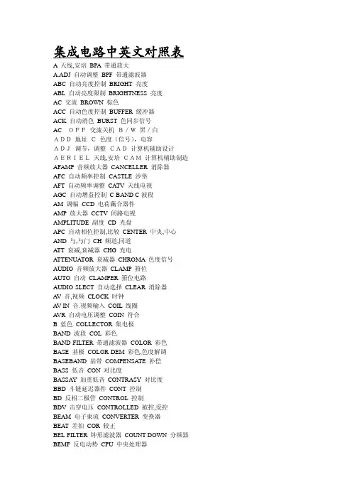
集成电路中英文对照表A天线,安培BPA带通放大A.ADJ自动调整BPF带通滤波器ABC自动亮度控制BRIGHT亮度ABL自动亮度限制BRIGHTNESS亮度AC交流BROWN棕色ACC自动色度控制BUFFER缓冲器ACK自动消色BURST色同步信号ACOFF交流关机B/W黑/白ADD地址C色度(信号),电容ADJ调节,调整CAD计算机辅助设计AERIEL天线,安培CAM计算机辅助制造AFAMP音频放大器CANCELLER消除器AFC自动频率控制CASTLE沙堡AFT自动频率调整CATV天线电视AGC自动增益控制C-BAND C-波段AM调幅CCD电荷藕合器件AMP放大器CCTV闭路电视AMPLITUDE副度CD光盘APC自动相位控制,比较CENTER中央,中心AND与,与门CH频道,同道ATT衰减,衰减器CHG充电ATTENUATOR衰减器CHROMA色度信号AUDIO音频放大器CLAMP箝位AUTO自动CLAMPER箝位电路AUDIO-SLECT自动选择CLEAR消除器A V音,视频CLOCK时钟A V-IN音.视频输入COIL线圈A VR自动电压调整COIN符合B蓝色COLLECTOR集电极BAND波段COL彩色BAND-FILTER带通滤波器COLOR彩色BASE基极COLOR-DEM彩色,色度解调BASEBAND基带COMPENSATE补偿BASS低音CON对比度BASSAY加重低音CONTRASY对比度BBD斗链延迟器件CONT控制BD反相二极管CONTROL控制BDV击穿电压CONTROLLED被控,受控BEAM电子束流CONVERTER变换器BEAT差拍COR较正BEL-FILTER钟形滤波器COUNT-DOWN分频器BEMF反电动势CPU中央处理器BF反馈CRT显像管BFO反馈振荡器CTV彩色电视机BIAS偏置CUT-OFF截止,切断,关机BLACK黑色CVBS复合全电视信号BLACK-STRETCH黑电平扩展,延伸DAC数模转换器BLANKING消隐DAGC延迟式自动增益控制BLK消隐DAMPING阻尼BLUE蓝色DARK黑暗,暗的BOARD板DATA数据,资料DB分贝FM-DISCRI调频鉴频器DC直流,直接藕合FOCUS聚焦DECODE®解码器FORCED强制的DEFEAT失效,无输出FRAME帧DEFL偏转FREQUENCY频率DEGAUSSER消磁器FREQ-ADJ频率调整DELAY延迟FUNC功能,作用DEMOD解调器FSC色副载波频率DEMONSTRATE演示FUSE保险丝DEMODULATOR解调器G绿色DET检波GAIN增益DETECTOR检波器GATE门,选通DEVIDER除法器GB国标DG微分增益GENERATOR发生器DIFF微分,差动GND地DIFFER-AMP差动放大器GP门控脉冲DIP双列直插塑料封装GREEN绿色DIS放电H行.水平DISCR鉴频器HALF-TONE半色调控制D.L延迟线HAR谐波DLY延迟H.BLK行消隐DOWN向下H.COIN行同步DP微分相位H.DRIVE行推动DRAM动态随机存取存储器HEATER灯丝DRIVE激励,驱动HF高频DRIVER激励器,驱动级HFA高频放大器DY偏转线圈HF-AMP高频放大器EARTH接地,地线HFC高频扼流器ECHO混响,回声HI-Q高品质因数EHT超高压HFO高频振荡器EHV超高压H-LOCK行锁定EMITTER发射极HOLD同步,保持ENCODE编码HOLD-IN同步,保持ENCODER编码器HOR行,水平的E2PROM电可擦可编程只读存储器H.COUNTDOWN行分频器EVEN偶数HOR DRIVER行推动器,驱动器EXT外接HOR.OSC行振荡器E/W东/西(枕较)HP高通,大功率FB反馈H.PARABOLA行抛物波F频率HPF高通滤波器FAST快速HTR灯丝FBL快速消隐HUE色.色彩.色调FBP快速消隐脉冲HVPS高压电源FBT行输出变压器HW半波FEED.BACK反馈HZ赫兹FIG图IAGC瞬时动做的自动增益控制FILTER滤波器IA VC瞬时动做的自动音量控制FILP-FLOP双稳态触发器IC集成电路FLY.BACK逆程I2C>BUS I2C总线FM调频ID识别,鉴别FM.DET调频检波IDENT识别,鉴别IF中频LOCK锁定IFAMP中频放大器LOCK IN锁住,同步IFT中频变压器LOOP环路IMMR维修,修理LOOPER斩波器IMPULSE脉冲LOW低,弱的IN英寸LPF低通病滤波器INPUT输入LSO行稳定振荡器INH反时钟方向的ISP行同步脉冲INSERTION插入MAIN主板INSTL安装MAINT维修,保养INT内.内部的MANUAL手动INTERGRTON集成,积分MARK符号INTERFACE接口,接口电路MASK屏蔽掩膜INTERLACING隔行扫描MATCH匹配INTERMEDATE中间,中频MATRIX矩阵INTAG积分,集成MATRIXER矩阵变换电路INTMT间断的MAX最大INVTR变换器MBF调制器带通滤波器I/O输入,输出M-D调制_解调IQ.DEMOD IQ信号解调MEMORY记忆.存储器ISOLATOR绝缘体.隔离器MHZ兆赫兹JUMP,飞线MIC话筒,麦克风JUNC连接器.连接点MIX混频,混合JUNGLE混合式MIXER混频器K-BAND K.波段MODE模式.状态KEY键MODULATOR调制器带通滤波器KEY-BOARD键盘MODULE模块.组件KEY.CODER键盘编码器MONITOR监视器KILLER消色器MONOCHROME单色的KINE电视显像管MONOSTABLE单稳态KP键控脉冲MOS金属氧化物半导体KEY.PULSE键控脉冲MOSFET场效应管L(CH)左声道,左通道MOST晶体管LAYOUT布线.电路布局MP维修点LED发光二极管MPL维修部分清单LIGHT发光二极管MPO最大功率输出LINEAR线性MRR维护.更换LEVEL电频,水平MSB最高位L.C.R电感.电容.电阻MULTSTANDARD多制式LD激光视盘MULTI.SYSTEM多制式LFA|低频放大器MULTI-TAP多抽头,插头MUSIC音乐MUTE静音LFF|LFO低频振荡器MVB多频振荡器LIMITER限幅器MVC手动音亮调节LINEAR线.线路MVS最小视频信号LINE.WIDTH行幅.线宽NAND与非门LIST目录.一览表NB窄频带LIVC低输入变换器NBFM窄带调频LIVCR低输入变换器及稳压器NC空脚.不接LOAD负载.输入加载NEG负的.负极行NEW新的PCB印刷电路板NF负反馈PCM脉冲编码调制NOISE噪声PD电位器NORTH北方PEAK峰值NOT非PP峰峰值NOT.GATE非门PEAKED>AMP峰值放大器NR噪声抑制PEAK_DET峰值检波器NTC-UNIT负温度系数元件PEM脉冲编码调制NTSC NTSC制式PF皮法拉NTI电路杂音干扰PHASE相位O输出PHASE>DET相位检波OC开路PHASE.CONTROL相位控制OCB过载断路器PHASE.SHIFTER移相器OCL无耦合电容输出电路PHASOR彩色信息矢量OSC周期变化的彩色顺序PHILIPS飞利浦ODD奇数.单数PHONIC声音的,有声的ODD-EVEN奇偶的PIF图像中频IC集成电路资料]:专业术语常用名词缩写中英文对照A:Actuator执行器A:Amplifier放大器A:Attendance员工考勤A:Attenuation衰减AA:Antenna amplifier开线放大器AA:Architectural Acoustics建筑声学AC:Analogue Controller模拟控制器ACD:Automatic Call Distribution自动分配话务ACS:ACCess Control System出入控制系统AD:Addressable Detector地址探测器ADM:Add/Drop Multiplexer分插复用器ADPCM:Adaptive Differential ulse Code Modulation自适应差分脉冲编码调制AF:Acoustic Feedback声反馈AFR:Amplitude/Frequency Response幅频响应AGC:Automati Gain Control自动增益控制AHU:Air Handling Unit空气处理机组A-I:Auto-iris自动光圈AIS:Alarm InDICation Signal告警指示信号AITS:Acknowledged Information Transfer Service确认操作ALC:Automati Level Control自动平衡控制ALS:Alarm Seconds告警秒ALU:Analogue Lines Unit模拟用户线单元AM:Administration Module管理模块AN:ACCess Network接入网ANSI:American National Standards Institute美国国家标准学会APS:Automatic Protection Switching自动保护倒换ASC:Automati Slope Control自动斜率控制ATH:Analogue Trunk Unit模拟中继单元ATM:Asynchrous Transfer Mode异步传送方式AU-PPJE:AU Pointer Positive Justification管理单元正指针调整AU:Administration Unit管理单元AU-AIS:Administrative Unit Alarm InDICation SignalAU告警指示信号AUG:Administration Unit Group管理单元组AU-LOP:Loss of Administrative Unit Pointer AU指针丢失AU-NPJE:AU Pointer Negative Justification管理单元负指针调整AUP:Administration Unit Pointer管理单元指针AVCD:Auchio&Video Control Device音像控制装置AWG:American Wire Gauge美国线缆规格BA:Bridge Amplifier桥接放大器BAC:Building Automation&Control net建筑物自动化和控制网络BAM:Background Administration Module后管理模块BBER:Background BLOCk Error Ratio背景块误码比BCC:B-channel Connect ControlB通路连接控制BD:Building DistributorBEF:Buiding Entrance Facilities建筑物入口设施BFOC:Bayonet Fibre Optic Connector大口式光纤连接器BGN:Background Noise背景噪声BGS:Background SOund背景音响BIP-N:Bit Interleaved Parity N code比特间插奇偶校验N位码B-ISDN:Brand band ISDN宽带综合业务数字网B-ISDN:Broad band-Integrated Services Digital Network宽带综合业务数字网BMC:Burst Mode Controller突发模式控制器BMS:Building Management System智能建筑管理系统BRI:Basic Rate ISDN基本速率的综合业务数字网BS:Base Station基站BSC:Base Station Controller基站控制器BUL:Back up lighting备用照明C/S:Client/Server客户机/服务器C:Combines混合器C:Container容器CA:Call ACCounting电话自动计费系统CATV:Cable Television有线电视CC:Call Control呼叫控制CC:Coax cable同轴电缆CCD:Charge coupled devices电荷耦合器件CCF:Cluster Contril Function簇控制功能CD:Campus Distributor建筑群配线架CD:Combination detector感温,感烟复合探测器CDCA:Continuous Dynamic Channel Assign连续的动态信道分配CDDI:Copper Distributed Data合同缆分布式数据接口CDES:Carbon dioxide extinguisbing system二氧化碳系统CDMA:Code Division Multiplex ACCess码分多址CF:Core Function核心功能CFM:Compounded Frequency Modulation压扩调频繁CIS:Call Information System呼叫信息系统CISPR:Internation Special Conmittee On Radio Interference国际无线电干扰专门委员会CLNP:Connectionless Network Protocol无连接模式网络层协议CLP:Cell Loss Priority信元丢失优先权CM:Communication Module通信模块CM:Configuration Management配置管理CM:Cross-connect Matrix交叉连接矩阵CMI:Coded Mark Inversion传号反转码CMISE:Common Management Information Service公用管理信息协议服务单元CPE:Convergence protocol entity会聚协议实体CR/E:Card reader/Encoder(Ticket reader)卡读写器/编码器CRC:Cyclic Redundancy Check循环冗佘校验CRT:Cathode Ray Tabe显示器,监视器,阴极射线管CS:Convergence service会聚服务CS:Cableron Spectrum旧纳档块化技术CS:Ceiling Screen挡烟垂壁CS:Convergence Sublayer合聚子层CSC:Combined Speaker Cabinet组合音响CSCW:Computer supported collaborative work计算机支持的协同工作CSES:Continuius Severely Errored Second连续严重误码秒CSF:Cell Site Function单基站功能控制CTB:Composite Triple Beat复合三价差拍CTD:Cable Thermal Detector缆式线型感温探测器CTNR:carrier to noise ratio载波比CW:Control Word控制字D:Directional指向性D:Distortion失真度D:Distributive分布式DA:Distribution Amplifier分配的大器DBA:Database Administrator数据库管理者DBCSN:Database Control System Nucleus数据库控制系统核心DBOS:Database Organizing System数据库组织系统DBSS:Database Security System数据库安全系统DC:Door Contacts大门传感器DCC:Digital Communication Channel数字通信通路DCN:Data Communication Network数据通信网DCP-I:Distributed Control Panel-Intelligent智能型分散控制器DCS:Distributed Control System集散型控制系统DDN:Digital Data Network数字数据网DDS:Direct Dignital Controller直接数字控制器DDW:Data Describing Word数据描述字DECT:Digital Enhanced Cordless Telecommunication增强数字无绳通讯DFB:Distributed Feedback分布反馈DID:Direct Inward Dialing直接中继方式,呼入直拨到分机用户DLC:Data Link Control Layer数据链路层DLI:DECT Line InterfaceDODI:Direct Outward Dialing One一次拨号音DPH:DECT PhoneDRC:Directional Response Cahracteristics指向性响应DS:Direct SOund直正声DSP:Digital signal Processing数字信号处理DSS:Deiision Support System决策支持系统DTMF:Dual Tone Multi-Frequency双音多频DTS:Dual-Technology SenSOr双鉴传感器DWDM:Dense Wave-length Division Multiplexing密集波分复用DXC:Digital Cross-Connect数字交叉连接E:Emergency lighting照明设备E:Equalizer均衡器E:Expander扩展器EA-DFB:Electricity AbSOrb-Distributed Feedback电吸收分布反馈ECC:Embedded Control Channel嵌入或控制通道EDFA:Erbium-Doped Fiber Amplifier掺饵光纤放大器EDI:Electronic Data Interexchange电子数据交换EIC:Electrical Impedance Characteristics电阻抗特性EMC:Electro Magnetic Compatibiloty电磁兼容性EMI:Electro Magnetic Interference电磁干扰EMS:Electromagnetic Sensitibility电磁敏感性EN:Equivalent Noise等效噪声EP:Emergency Power应急电源ES:Emergency SOoket应急插座ES:Evacuation Sigvial疏散照明ESA:Error SecondA误码秒类型AESB:ErrorSecondB误码秒类型BESD:Electrostatic Discharge静电放电ESR:Errored Second Ratio误码秒比率ETDM:Electrical Time Division Multiplexing电时分复用ETSI:European Telecommunication Standards Institute欧洲电信标准协会F:Filter滤波器FAB:Fire Alarm Bell火警警铃FACU:Fire Alarm Contrlol Unit火灾自动报警控制装置FC:Failure Count失效次数FC:Frequency Converter频率变换器FCC:Fire Alarm System火灾报警系统FCS:Field Control System现场总线FCU:Favn Coil Unit风机盘管FD:Fire Door防火门FD:Flame Detector火焰探测器FD:Floor DistributorFD:Frequency Dirsder分频器FDD:Frequency Division Dual频分双工FDDI:Fiberdistributed Data Interface光纤缆分布式数据接口。
封装形式:封装形式是指安装半导体集成电路芯片用的外壳。
它不仅起着安装、固定、密封、保护芯片及增强电热性能等方面的作用,而且还通过芯片上的接点用导线连接到封装外壳的引脚上,这些引脚又通过印刷电路板上的导线与其他器件相连接。
衡量一个芯片封装技术先进与否的重要指标是芯片面积与封装面积之比,这个比值越接近1越好。
封装大致经过了如下发展进程:结构方面:TO->DIP->LCC->QFP->BGA ->CSP;材料方面:金属、陶瓷->陶瓷、塑料->塑料;引脚形状:长引线直插->短引线或无引线贴装->球状凸点;装配方式:通孔插装->表面组装->直接安装。
常见英文缩写解释(按字母顺序排列):产品命名规则模拟滤波器 光纤通信 高速信号处理和转换 无线/射频 光线通讯,模拟 显示支持电路 高频模拟和混合信号ASIC 数字转换器,接口,电源管理,电池监控 DC/DC 电源 电压基准MAXIM 前缀是“MAX”。
DALLAS 则是以“DS ”开头。
MAX ×××或MAX ××××说明:1后缀CSA 、CWA 其中C 表示普通级,S 表示表贴,W 表示宽体表贴。
2 后缀CWI 表示宽体表贴,EEWI 宽体工业级表贴,后缀MJA 或883为军级。
3 CPA 、BCPI 、BCPP 、CPP 、CCPP 、CPE 、CPD 、ACPA 后缀均为普通双列直插。
举例MAX202CPE 、CPE 普通ECPE 普通带抗静电保护MAX202EEPE 工业级抗静电保护(-45℃-85℃) 说明 E 指抗静电保护 MAXIM 数字排列分类1字头 模拟器 2字头 滤波器 3字头 多路开关 4字头 放大器 5字头 数模转换器 6字头 电压基准 7字头 电压转换 8字头 复位器 9字头 比较器DALLAS 命名规则例如DS1210N.S. DS1225Y-100IND N=工业级S=表贴宽体 MCG=DIP 封 Z=表贴宽体 MNG=DIP 工业级 IND=工业级 QCG=PLCC 封 Q=QFP下面是MAXIM 的命名规则: 三字母后缀: 例如:MAX358CPDC = 温度范围 P = 封装类型D = 管脚数温度范围:C = 0℃ 至 70℃ (商业级) I = -20℃ 至 +85℃ (工业级) E = -40℃ 至 +85℃ (扩展工业级) A = -40℃ 至 +85℃ (航空级) M = -55℃ 至 +125℃ (军品级)封装类型:A SSOP(缩小外型封装)B CERQUAD四字母后缀: 例如:MAX1480ACPIA = 指标等级或附带功能 C = 温度范围 P = 封装类型 I = 管脚数管脚数:A: 8 B: 10,64 C: 12,192 D: 14E: 16 F: 22,256 G: 24 H: 44 I: 28 J: 32 K: 5,68 L: 40 M: 7,48 N: 18 O: 42 P: 20 Q: 2,100 R: 3,84 S: 4,80 T: 6,160 U: 60 V: 8(圆形) W: 10(圆形) X: 36Y: 8(圆形) Z: 10(圆形)C TO-220, TQFP(薄型四方扁平封装)D 陶瓷铜顶封装E 四分之一大的小外型封装F 陶瓷扁平封装H 模块封装, SBGA(超级球式栅格阵列, 5x5 TQFP)J CERDIP (陶瓷双列直插)K TO-3 塑料接脚栅格阵列L LCC (无引线芯片承载封装)M MQFP (公制四方扁平封装)N 窄体塑封双列直插P 塑封双列直插Q PLCC (塑料式引线芯片承载封装)R 窄体陶瓷双列直插封装(300mil)S 小外型封装T TO5,TO-99,TO-100U TSSOP,μMAX,SOTW 宽体小外型封装(300mil)X SC-70(3脚,5脚,6脚)Y 窄体铜顶封装Z TO-92,MQUAD/D 裸片/PR 增强型塑封/W 晶圆DSP信号处理器放大器工业用器件通信电源管理移动通信视频/图像处理器等模拟A/D D/A 转换器传感器模拟器件AD产品以“AD”、“ADV”居多,也有“OP”或者“REF”、“AMP”、“SMP”、“SSM”、“TMP”、“TMS”等开头的。
电子行业电子英文翻译介绍随着国际间贸易的不断发展和深入,电子行业也变得越来越国际化。
在与国外公司合作或进行技术交流时,电子行业常常需要进行电子英文翻译,以便更好地沟通交流。
本文将介绍电子行业中常见的英文术语,以及如何进行准确和专业的电子英文翻译。
电子行业常用英文术语在进行电子英文翻译时,了解电子行业常用的英文术语是非常重要的。
以下是一些常见的电子行业英文术语:1.Integrated Circuit (IC):集成电路2.Printed Circuit Board (PCB):印刷电路板3.Resistor:电阻器4.Capacitor:电容器5.Transistor:晶体管6.Diode:二极管7.Microcontroller:微控制器8.Oscillator:振荡器9.Connector:连接器10.S witch:开关11.P ower Supply:电源12.A mplifier:放大器13.S ensor:传感器14.L ED (Light Emitting Diode):发光二极管15.L CD (Liquid Crystal Display):液晶显示屏以上仅是一些常见的电子行业英文术语,电子行业还有许多其他专业术语,根据需要进行适当的补充。
电子英文翻译的技巧在进行电子英文翻译时,以下是一些技巧和建议,以保证翻译的准确性和专业性:1. 理解上下文在进行电子英文翻译时,首先要理解原文所处的上下文。
根据上下文的不同,同一个术语可能有不同的翻译,因此需要根据具体情况进行判断和选择。
2. 使用专业术语电子行业有许多专业术语,尽可能使用原汁原味的英文术语,以保持翻译的专业性。
如果有必要,可以附上相应的中文解释,以便读者更好地理解。
3. 确保准确性电子行业术语的翻译必须保证准确无误。
在进行翻译时,可以参考相关的标准和行业规范,确保翻译的准确性。
4. 使用在线资源在进行电子英文翻译时,可以借助各种在线资源,如术语在线词典、行业技术论坛等。
常见电子专业术语中英文对照常见英文缩写解释(按字母顺序排列):ASIC:Application Specific Integrated Circuit。
专用ICCPLD:Complex Programmable Logic Device. 复杂可编程逻辑器件EDA: Electronic Design Automation. 电子设计自动化FPGA:Field Programmable Gate Array。
现场可编程门阵列GAL: Generic Array Logic. 通用阵列逻辑HDL: Hardware Description Language。
硬件描述语言IP: Intelligent Property。
智能模块PAL: Programmable Array Logic. 可编程阵列逻辑RTL: Register Transfer Level. 寄存器传输级描述)SOC: System On a Chip. 片上系统SLIC:System Level IC。
系统级ICVHDL:Very high speed integrated circuit Hardware Description Language. 超高速集成电路硬件描述语言AASIC(专用集成电路)Application-Specific Integrated Circuit. A piece of custom-designed hardware in a chip.专用集成电路。
一个在一个芯片上定制设计的硬件。
address bus (地址总线)A set of electrical lines connected to the processor and all of the peripher als withwhich itcommunicates。
The address bus is used by the processor to select aspecific memory location or register within a particular peripheral。
集成电路常见名词缩写中英对照(入门篇)SoC--------------系统化芯片SoP-----------------封装上的系统ASIC------------特定用途集成电路ADC-------------模数转换器DAC-------------数模转换器PLL--------------锁相环PMU-------------电源管理单元DSP--------------数字信号处理SRAM-----------静态处理器ROM-----------------只读存储器AFE--------------模拟前端PHY--------------物理层SATA-------------串行高级技术附件IP------------------知识产权(不指互联网协议)HDMI-------------高清晰度多媒体接口MEMS------------微机电系统RF-----------------射频LVDS-------------低压差分信号GPIO--------------通用输入输出PWB----------------印刷线路板DLL-----------------延迟锁定环GPU-----------------图形处理器CAM----------------内容可寻址存储器RSDS----------------低摆幅差分信号DVI------------------数字视频接口DDR(DDR SDRAM)------双倍速率同步动态随机存储器wafer----------------晶圆die--------------------裸片chip------------------芯片四大晶圆代工厂TSMC---------------台积电UMC-----------------联电SMIC----------------中芯国际Chartered------------特许半导体。

【集成电路(IC)】电子专业术语英汉对照加注解电子专业英语术语★rchitecture(结构):可编程集成电路系列的通用逻辑结构。
★ASIC(Application Specific Integrated Circuit-专用集成电路):适合于某一单一用途的集成电路产品。
★ATE(Automatic Test EQUIPment-自动测试设备):能够自动测试组装电路板和用于莱迪思ISP 器件编程的设备。
★BGA(Ball Grid Array-球栅阵列):以球型引脚焊接工艺为特征的一类集成电路封装。
可以提高可加工性,减小尺寸和厚度,改善了噪声特性,提高了功耗管理特性。
★Boolean Equation(逻辑方程):基于逻辑代数的文本设计输入方法。
★Boundary Scan Test(边界扫描测试):板级测试的趋势。
为实现先进的技术所需要的多管脚器件提供了较低的测试和制造成本。
★Cell-Based PLD(基于单元的可编程逻辑器件):混合型可编程逻辑器件结构,将标准的复杂的可编程逻辑器件(CPLD)和特殊功能的模块组合到一块芯片上。
★CMOS(Complementary Metal Oxide Semiconductor-互补金属氧化物半导体):先进的集成电路★加工工艺技术,具有高集成、低成本、低能耗和高性能等特征。
CMOS 是现在高密度可编程逻辑器件(PLD)的理想工艺技术。
★CPLD(Complex Programmable Logic Device-复杂可编程逻辑器件):高密度的可编程逻辑器件,包含通过一个中央全局布线区连接的宏单元。
这种结构提供高速度和可预测的性能。
是实现高速逻辑的理想结构。
理想的可编程技术是E2CMOS?。
★Density (密度):表示集成在一个芯片上的逻辑数量,单位是门(gate)。
密度越高,门越多,也意味着越复杂。
★Design Simulation(设计仿真):明确一个设计是否与要求的功能和时序相一致的过程。
芯片行业常用英文术语最详细总结在当今信息时代,芯片产业扮演着至关重要的角色。
无论是计算机、手机、汽车还是物联网设备,芯片无处不在。
而要深入了解芯片产业,首先需要了解其中常用的英文术语。
本文将从浅入深,为您详细总结芯片行业常用的英文术语,帮助您更全面地理解这一领域。
1. Integrated Circuit (IC)Integrated Circuit,即集成电路,是芯片行业最基本的术语之一。
它指的是在一个小块半导体材料上集成了大量传统电路元件的一种电子元件。
IC的发明极大地推动了电子技术的进步,是现代电子产品的基础。
2. Semiconductor半导体是指导电性介于导电体和绝缘体之间的材料。
在芯片行业中,半导体材料被广泛应用于制造集成电路等电子元件。
要理解芯片行业,对半导体的特性和应用有深入了解是至关重要的。
3. Microprocessor微处理器是一种包含了中央处理器功能的集成电路。
它是电子设备的大脑,负责执行计算机程序中的指令。
微处理器的性能直接影响着设备的运行速度和处理能力。
4. Semiconductor Memory半导体存储器是一种能够存储数据的半导体器件。
在芯片行业中,常见的半导体存储器包括随机存取存储器(RAM)和只读存储器(ROM),它们在计算机和其他电子设备中被广泛应用。
5. Field-Programmable Gate Array (FPGA)现场可编程门阵列是一种基于半导体技术的可编程逻辑器件。
它可以根据用户的需要进行重新编程,具有灵活性和可重构性的特点,被广泛应用于数字电路设计和信号处理领域。
6. System on a Chip (SoC)片上系统是一种集成了多个功能模块的芯片。
它包括了处理器核心、存储器、输入输出接口等多个组件,能够实现多种功能。
SoC的出现极大地提高了电子设备的集成度和性能。
7. Semiconductor Manufacturing半导体制造是芯片行业的基础,它涉及到原料的提纯、器件的制造和芯片的封装测试等多个环节。

电子电路术语中英文对照电子电路术语中英文对照电子电路术语中英文对照AC(alternating current) 交流(电)ACPI(Advanced Configuration and Power Interface)高级配置电源界面A/D(analog to digital) 模拟/数字转换ADC(analog to digital convertor) 模拟/数字转换器ADM(adaptive delta modulation) 自适应增量调制ADPCM(adaptive differential pulse code modulation) 自适应差分脉冲编码调制ALU(arithmetic logic unit) 算术逻辑单元AM(Amplitude Modulation)调幅ASCII(American standard code for information interchange) 美国信息交换标准码ATA(Advanced Technology Attachment)高级技术附加装置AV(audio visual) 声视,视听BCD(binary coded decimal) 二进制编码的十进制数BCR(bi-directional controlled rectifier)双向晶闸管BCR(buffer courtier reset) 缓冲计数器BIOS(Basic Input Output System) 基本输入输出系统BZ(buzzer) 蜂鸣器,蜂音器C(capacitance,capacitor) 电容量,电容器CATV(cable television) 电缆电视CCD(charge-coupled device) 电荷耦合器件CCTV(closed-circuit television) 闭路电视CMOS(complementary) 互补MOSCPU(central processing unit)中央处理单元CS(control signal) 控制信号D(diode) 二极管DAST(direct analog store technology) 直接模拟存储技术DC(direct current) 直流DIP(dual in-line package) 双列直插封装DP(dial pulse) 拨号脉冲DRAM(dynamic random access memory) 动态随机存储器DTL(diode-transistor logic) 二极管晶体管逻辑DUT(device under test) 被测器件DVM(digital voltmeter) 数字电压表ECG(electrocardiograph) 心电图ECL(emitter coupled logic) 射极耦合逻辑EDI(electronic data interchange) 电子数据交换EIA(Electronic Industries Association) 电子工业联合会EIDE(Enhanced Integrated Drive Electronics)增强集成电路设备EOC(end of conversion) 转换结束EPROM(erasable programmable read only memory) 可擦可编程只读存储器EEPROM(electrically EPROM) 电可擦可编程只读存储器ESD(electro-static discharge) 静电放电FET(field-effect transistor) 场效应晶体管FS(full scale) 满量程F/V(frequency to voltage convertor) 频率/电压转换FLTA(Foreign Language Teaching Agency)上海外教网FM(frequency modulation) 调频FSK(frequency shift keying) 频移键控FSM(field strength meter) 场强计FST(fast switching shyster) 快速晶闸管FT(fixed time) 固定时间FU(fuse unit) 保险丝装置FWD(forward) 正向的GAL(generic array logic) 通用阵列逻辑GND(ground) 接地,地线GPU(Graphic Process Unit)图形处理单元/图形处理器GTO(Sate turn off thruster) 门极可关断晶体管HART(highway addressable remote transducer) 可寻址远程传感器数据公路HCMOS(high density COMS) 高密度互补金属氧化物半导体(器件)HDD(hard disk drive)硬盘驱动器HF(high frequency) 高频HIFI(High-Fidelity)高保真HTL(high threshold logic) 高阈值逻辑电路HTS(heat temperature sensor) 热温度传感器IC(integrated circuit) 集成电路ID(international data) 国际数据IDE (Integrated Drive Electronics)集成电路设备IGBT(insulated gate bipolar transistor) 绝缘栅双极型晶体管IGFET(insulated gate field effect transistor) 绝缘栅场效应晶体管I/O(input/output) 输入/输出I/V(current to voltage convertor) 电流-电压变换器IPM(incidental phase modulation) 附带的相位调制IPM(intelligent power module) 智能功率模块IR(infrared radiation) 红外辐射IRQ(interrupt request) 中断请求ISA( Industry Standard Architecture) 工业标准结构JFET(junction field effect transistor) 结型场效应晶体管LAS(light activated switch)光敏开关LASCS(light activated silicon controlled switch) 光控可控硅开关LCD(liquid crystal display) 液晶显示器LDR(light dependent resistor) 光敏电阻LED(light emitting diode) 发光二极管LRC(longitudinal redundancy check) 纵向冗余(码)校验LSB(least significant bit) 最低有效位LSI(1arge scale integration) 大规模集成电路M(motor) 电动机MCT(MOS controlled gyrator) 场控晶闸管MIC(microphone) 话筒,微音器,麦克风min(minute) 分MOS(metal oxide semiconductor)金属氧化物半导体MOSFET(metal oxide semiconductor FET) 金属氧化物半导体场效应晶体管N(negative) 负NMOS(N-channel metal oxide semiconductor FET) N 沟道MOSFETNTC(negative temperature coefficient) 负温度系数OC(over current) 过电流OCB(overload circuit breaker) 过载断路器OCS(optical communication system) 光通讯系统OR(type of logic circuit) 或逻辑电路OV(over voltage) 过电压P(pressure) 压力FAM(pulse amplitude modulation) 脉冲幅度调制PATA(Parallel Advanced Technology Attachment)串行ATAPC(pulse code) 脉冲码PCI(Peripheral Component Interconnect)外设部件互连标准PCM(pulse code modulation) 脉冲编码调制PDM(pulse duration modulation) 脉冲宽度调制PF(power factor) 功率因数PFM(pulse frequency modulation) 脉冲频率调制PG(pulse generator) 脉冲发生器PGM(programmable) 编程信号PI(proportional-integral(controller)) 比例积分(控制器)PID(proportional-integral-differential(contro ller))比例积分微分(控制器)PIN(positive intrinsic-negative) 光电二极管PIO(parallel input output) 并行输入输出PLD(phase-locked detector) 同相检波PLD(phase-locked discriminator) 锁相解调器PLL(phase-locked loop) 锁相环路PMOS(P-channel metal oxide semiconductor FET) P 沟道MOSFETP-P(peak-to-peak) 峰--峰PPM(pulse phase modulation) 脉冲相位洲制PRD(piezoelectric radiation detector) 热电辐射控测器PROM(programmable read only memory) 可编只读程存储器PRT(platinum resistance thermometer) 铂电阻温度计PRT(pulse recurrent time) 脉冲周期时间PUT(programmable unijunction transistor) 可编程单结晶体管PWM(pulse width modulation) 脉宽调制R(resistance,resistor) 电阻,电阻器RAM(random access memory) 随机存储器RCT(reverse conducting thyristor) 逆导晶闸管REF(reference) 参考,基准REV(reverse) 反转R/F(radio frequency) 射频RGB(red/green/blue) 红绿蓝ROM(read only memory) 只读存储器RP(resistance potentiometer) 电位器RST(reset) 复位信号RT(resistor with inherent variability dependent)热敏电阻RTD(resistance temperature detector) 电阻温度传感器RTL(resistor transistor logic) 电阻晶体管逻辑(电路)RV(resistor with inherent variability dependent on the voltage) 压敏电阻器SA(switching assembly) 开关组件SBS(silicon bi-directional switch) 硅双向开关,双向硅开关SCR(silicon controlled rectifier) 可控硅整流器SCS(safety control switch) 晶体管-晶体管逻辑(电路) 安全控制开关SCS(silicon controlled switch) 可控硅开关SCS(speed control system) 速度控制系统SCS(supply control system) 电源控制系统SG(spark gap) 放电器SIT(static induction transformer) 静电感应晶体管SITH(static induction thyristor) 静电感应晶闸管SP(shift pulse) 移位脉冲SPI(serial peripheral interface) 串行外围接口SR(sample realy,saturable reactor) 取样继电器,饱和电抗器SR(silicon rectifier) 硅整流器SRAM(static random access memory) 静态随机存储器SSR(solid-state relay) 固体继电器SSR(switching select repeater) 中断器开关选择器SSS(silicon symmetrical switch) 硅对称开关,双向可控硅SSW(synchro-switch) 同步开关ST(start) 启动ST(starter) 启动器STB(strobe) 闸门,选通脉冲T(transistor) 晶体管,晶闸管TACH(tachometer) 转速计转速表TP(temperature probe) 温度传感器TRIAC(triodes AC switch) 三极管交流开关TTL(Transistor-Transistor Logic) 晶体管-晶体管逻辑(电路)TV(television) 电视UART(universal asynchronous receiver transmitter) 通用异步收发器UPS(Uninterrupted Power Supply)不间断电源USB(Universal Serial Bus)通用串行接口VCO(voltage controlled oscillator) 压控振荡器VD(video decoders) 视频译码器VDR(voltage dependent resistor) 压敏电阻VF(video frequency) 视频V/F(voltage-to-frequency) 电压/频率转换V/I(voltage to current convertor) 电压-电流变换器VM(voltmeter) 电压表VS(vacuum switch) 电子开关VT(visual telephone) 电视电话VT(video terminal) 视频终端WIFI(Wireless Fidelity)802.11b标准。
集成电路行业专业名词解释集成电路(Integrated Circuit,IC)是一种将大量电子元件集成、封装在一个微小的硅片上的技术。
集成电路可以实现多种电子功能,并且具有高度的可靠性和稳定性。
它是现代电子技术发展中的重要组成部分。
芯片(Chip)是指集成电路中的核心部件,它包含了电子元件和电路连接线路的图案。
芯片的制作通常采用微影技术,将电路图案镀刻到硅片上。
根据功能和规模的不同,芯片可以分为逻辑芯片、存储芯片、模拟芯片等。
VLSI(Very Large Scale Integration)是指超大规模集成电路。
VLSI技术使得更多的电子元件能够被集成在一块芯片上,从而实现更复杂的电子功能。
随着技术的不断进步,集成度越来越高,芯片上的晶体管数量也越来越多。
目前,VLSI已经成为集成电路行业的主要发展方向。
SoC(System on a Chip)是指一种将整个系统集成在一块芯片上的技术。
这种芯片通常包括处理器、内存、输入输出接口等多个电子组件。
SoC技术在嵌入式系统和移动设备领域得到广泛应用,它的好处是可以提高系统性能、降低功耗和成本。
测试与封装(Test and Packaging)是指对集成电路进行功能测试和封装的过程。
功能测试是为了验证芯片是否按设计要求正常工作,封装则是将芯片放入适当的封装中,以保护芯片并提供电路连接。
测试与封装是集成电路生产中的重要环节,它们对产品质量和性能起着关键作用。
以上是集成电路行业常用的专业名词解释。
集成电路作为现代电子技术的核心,对于我们的生活和工作产生了深远的影响。
通过了解这些专业名词,可以更好地理解和应用集成电路技术,推动行业的进步和发展。
集成电路设计专业名词解释汇总英文版English:"Integrated Circuit (IC) Design: The process of creating a blueprint for the manufacturing of integrated circuits, such as microchips, using specialized software and tools. IC design involves several stages, including architectural design, logic design, circuit design, physical design, and verification. Architectural design establishes the high-level functionality and organization of the circuit, determining the overall structure and major components. Logic design involves the translation of the architectural design into a set of logic equations and functional blocks, specifying the logical operation of the circuit. Circuit design focuses on the actual implementation of the logic design, defining the electrical connections and components needed to achieve the desired functionality. Physical design, also known as layout design, involves the placement and routing of the components to ensure proper functioning and optimal performance, considering factors such as power consumption, signal integrity, and manufacturing constraints. Verification is the process of ensuring that the designed circuit meets the specified requirements and functions correctly under various conditions. Field-ProgrammableGate Array (FPGA): An integrated circuit that can be configured by the user after manufacturing. FPGAs contain an array of programmable logic blocks and interconnects, allowing for the implementation of various digital circuits. Hardware Description Language (HDL): A specialized programming language used to describe the behavior and structure of electronic circuits, facilitating the design and simulation of digital systems. Common HDLs include Verilog and VHDL. Electronic Design Automation (EDA) Tools: Software tools used in the design of electronic systems, including integrated circuits. EDA tools automate various stages of the design process, from schematic capture and simulation to layout and verification. Some popular EDA tools include Cadence Virtuoso, Synopsys Design Compiler, and Mentor Graphics Calibre. Very-Large-Scale Integration (VLSI): The process of integrating thousands or millions of transistors into a single chip. VLSI technology enables the creation of complex, high-performance integrated circuits, such as microprocessors and memory chips, by packing a large number of transistors into a small area. Application-Specific Integrated Circuit (ASIC): An integrated circuit customized for a particular application or purpose. Unlike FPGAs, ASICs are manufactured to perform a specific function, offering advantages in terms of performance,power consumption, and cost for mass production. ASIC design involves the development of custom circuitry optimized for a particular application, often using standard cell libraries and specialized design methodologies."中文翻译:"集成电路(IC)设计:是指利用专业软件和工具创建集成电路(如微芯片)制造的蓝图的过程。
电子技术基本词汇Chapter 7 analog signals 模拟信号digital signals 数字信号Sequential Logic Circuits 时序逻辑电路Combinatorial Logic Circuits 组合逻辑电路Chip 芯片Integrated circuits (IC) 集成电路Boolean algebra 布尔代数Boolean variables 布尔变量Synthesis of Logic Circuits组合逻辑电路综合analysis of Logic Circuits组合逻辑电路分析De Morgan’s Laws德摩根律Gate circuit 门电路Minterms 最小项Maxterms 最大项Sum-of-Products 与或表达式Product-of-Sums 或与表达式Logic diagram 逻辑电路图Logic function 逻辑函数Truth table 真值表Encoders 编码器Decoders 译码器Karnaugh Maps 卡诺图Flip-flop 触发器Clock Signal 时钟信号Synchronous 同步Asynchronous 异步positive-edge-triggered 上升沿触发negative-edge-triggered下降沿触发Shift Register 移位寄存器Counter 计数器Binary counter 二进制计数器Decimal counter十进制计数器Chapter 8 Carriers 载流子Diode 二极管Semiconductor 半导体pn junction pn结hole 空穴electron 电子Saturation current 饱和电流Thermal voltage 热电压Anode 阳极Cathode 阴极Forward/ reverse bias 前向/反向偏置Zener Diode 齐纳/稳压二极管operating point 工作点Rectifier circuits 整流电路Filter circuits 滤波电路Half-wave rectifier 半波整流电路Full-wave rectifier 全波整流电路Clipper Circuits 限幅/削波电路Clamp Circuits钳位电路Small-signal Equivalent Circuits 小信号等效电路Chapter 9 Amplifiers 放大器/放大电路Cascaded Amplifiers 级联放大器Amplitude 幅值Phase 相位Inverting amplifiers 反相放大电路Noninverting amplifiers 同相放大电路Voltage-Amplifier 电压放大电路Current-Amplifier 电流放大电路Transconductance -Amplifier 跨导放大电路Transresistance-Amplifier 互阻放大电路Gain 增益Current/voltage/power gain 电流/电压/功率增益Input/output resistance 输入/输出电阻Loading Effects 负载效应AC Coupling 交流耦合Direct Coupling 直接(直流)耦合Phase/Waveform Distortion 相位/波形失真(畸变)Transfer Characteristic 转移特性Differential Amplifiers 差分放大电路inverting input 反相输入端noninverting input 同相输入端Differential Signal 差分(模)信号Common-mode Signal 共模信号Common Mode Rejection Ratio (CMRR)共模抑制比Bias Current 偏置电流Offset Voltage 失调电压Offset Current 失调电流Complementary symmetry power amplifiers 互补对称功率放大电路Feedback 反馈Half-power Frequency 半功率频率Low frequency region 低频区Midband frequency region 中频区high frequency region 高频区Pulse Response 脉冲响应Harmonic Distortion 谐波失真Chapter 10Transistors 晶体管Field-Effect Transistors (FET) 场效应晶体管Metal-oxide-semiconductor MOSFET 金属氧化物半导体场效应晶体管n-Channel Enhancement n沟道增强型Grid 栅极Source源极Drain漏极Base 衬底Cutoff Region 截止区Triode Region 三角区/可变电阻区Saturation Region 饱和区Bias Circuits 偏置电路The Fixed- Plus Self-Bias Circuit 固定增益自偏置电路Transconductance 跨导Drain Resistance 漏极电阻Common-source Amplifiers 共源极放大电路bypass capacitor 旁通电容coupling capacitor 耦合电容Source Followers 源极跟随器CMOS 互补对称MOS管Chapter 11Bipolar Junction Transistors (BJT) 双极型晶体管Triode Tube 三极管base collector p-n junction 基集pn结(集电结)base emitter p-n junction 基射pn结(发射结)fixed base bias circuit 固定偏置电路Four-Resistor bias Circuit 四电阻偏置电路/分压偏置电路Active region 线性放大区Common-Emitter 共发射极Emitter Followers 射极跟随器nonlinear distortion 非线性畸变Chapter 12Operational Amplifiers 运算放大器Infinite gain 无穷大增益Summing-point Constraint 结点约束(加和点约束) Virtual short 虚短Virtual open 虚断negative feedback 负反馈positive feedback 正反馈Serial/parallel feedback 串联/并联反馈Bandwidth 带宽open-loop gain 开环增益closed-loop gain 闭环增益Output Voltage Swing 输出电压幅值限制Output Current Limits 输出电流限制Slew-Rate Limitation 转换速率限制Full-power bandwidth 全功率带宽Integrators 积分器Differentiators 微分器。
Integrated circuit (IC)IntroducionIntegrated circuit also called microelectronic circuit or chip an assembly of electronic components, fabricated as a single unit, in which miniaturized active devices (e.g., transistors and diodes) and passive devices (e.g., capacitors and resistors) and their interconnections are built up on a thin substrate of semiconductor material (typically silicon). The resulting circuit is thus a small monolithic “chip,” which may be as small as a few square centimetres or only a few square millimetres. The individual circuit components are generally microscopic in size.Integrated circuits have their origin in the invention of the transistor in 1947 by William B. Shockley and his team at the American Telephone and Telegraph Company's Bell Laboratories. Shockley's team (including John Bardeen and Walter H. Brattain) found that, under the right circumstances, electrons would form a barrier at the surface of certain crystals, and they learned to control the flow of electricity through the crystal by manipulating this barrier. Controlling electron flow through a crystal allowed the team to create a device that could perform certain electrical operations, such as signal amplification, that were previously done by vacuum tubes. They named this device a transistor, from a combination of the words transfer and resistor (see photograph). The study of methods of creating electronic devices using solid materials became known as solid-state electronics. Solid-state devices proved to bemuch sturdier, easier to work with, more reliable, much smaller, and less expensive than vacuum tubes.Using the same principles and materials, engineers soon learned to create other electrical components, such as resistors and capacitors. Now that electrical devices could be made so small, the largest part of a circuit was the awkward wiring between the devices.In 1958 Jack Kilby of Texas Instruments, Inc., and Robert Noyce of Fairchild Semiconductor Corporation independently thought of a way to reduce circuit size further. They laid very thin paths of metal (usually aluminum or copper) directly on the same piece of material as their devices. These small paths acted as wires. With this technique an entire circuit could be “integrated” on a single piece of sol id material and an integrated circuit (IC) thus created. ICs can contain hundreds of thousands of individual transistors on a single piece of material the size of a pea. Working with that many vacuum tubes would have been unrealistically awkward and expensive. The invention of the integrated circuit made technologies of the Information Age feasible. ICs are now used extensively in all walks of life, from cars to toasters to amusement park rides.Basic IC typesAnalog versus digital circuitsAnalog, or linear, circuits typically use only a few components and are thus some of the simplest types of ICs. Generally, analog circuits are connected to devices that collect signals from the environment or send signals back to theenvironment. For example, a microphone converts fluctuating vocal sounds into an electrical signal of varying voltage. An analog circuit then modifies the signal in some useful way—such as amplifying it or filtering it of undesirable noise. Such a signal might then be fed back to a loudspeaker, which would reproduce the tones originally picked up by the microphone.Another typical use for an analog circuit is to control some device in response to continual changes in the environment. For example, a temperature sensor sends a varying signal to a thermostat, which can be programmed to turn an air conditioner, heater, or oven on and off once the signal has reached a certain value.A digital circuit, on the other hand, is designed to accept only voltages of specific given values. A circuit that uses only two states is known as a binary circuit. Circuit design with binary quantities, “on” and “off” representing 1 and 0 (i.e., true and false), uses the logic of Boolean algebra. The three basic logic functions—NOT, AND, and OR—together with their truth tables are given in the figure. (Arithmetic is also performed in the binary number system employing Boolean algebra.) These basic elements are combined in the design of ICs for digital computers and associated devices to perform the desired functions.Microprocessor circuitsMicroprocessors are the most complicated ICs. They are composed of millions of transistors that have been configuredas thousands of individual digital circuits, each of which performs some specific logic function. A microprocessor is built entirely of these logic circuits synchronized to each other.Just like a marching band, the circuits perform their logic function only on direction by the bandmaster. The bandmaster in a microprocessor, so to speak, is called the clock. The clock is a signal that quickly alternates between two logic states. Every time the clock changes state, every logic circuit in the microprocessor does something. Calculations can be made very quickly, depending on the speed (“clock frequency”) of the microprocessor.Microprocessors contain some circuits, known as registers, that store information. Registers are predetermined memory locations. Each processor has many different types of registers. Permanent registers are used to store the preprogrammed instructions required for various operations (such as addition and multiplication). Temporary registers store numbers that are to be operated on and also the result. Other examples of registers include the “program counter,” the “stack pointer,” and the “address” register.Microprocessors can perform millions of operations per second on data. In addition to computers, microprocessors are common in video game systems, televisions, cameras, and automobiles.Memory circuitsMicroprocessors typically have to store more data than can be held in a few registers. This additional information isrelocated to special memory circuits. Memory is composed of dense arrays of parallel circuits that use their voltage states to store information. Memory also stores the temporary sequence of instructions, or program, for the microprocessor. Manufacturers continually strive to reduce the size of memory circuits—to increase capability without increasing space. In addition, smaller components typically use less power, operate more efficiently, and cost less to manufacture.Digital signal processorsA signal is an analog waveform—anything in the environment that can be captured electronically. A digital signal is an analog waveform that has been converted into a series of binary numbers for quick manipulation. As the name implies, a digital signal processor (DSP) processes signals digitally, as patterns of 1s and 0s. For instance, using an analog-to-digital converter, commonly called an A-to-D or A/D converter, a recording of someone's voice can be converted into digital 1s and 0s. The digital representation of the voice can then be modified by a DSP using complex mathematical formulas. For example, the DSP algorithm in the circuit may be configured to recognize gaps between spoken words as background noise and digitally remove ambient noise from the waveform. Finally, the processed signal can be converted back (by a D/A converter) into an analog signal for listening. Digital processing can filter out background noise so fast that there is no discernible delay and the signal appears to be heard in “real time.” For instance, such processing enables “live” televisionbroadcasts to focus on a quarterback's signals in an American gridiron football game. DSPs are also used to produce digital effects on live television. For example, the yellow marker lines displayed during the football game are not really on the field; a DSP adds the lines after the cameras shoot the picture but before it is broadcast. Similarly, some of the advertisements seen on stadium fences and billboards during televised sporting events are not really there.Application-specific ICsAn application-specific IC (ASIC) can be either a digital or an analog circuit. As their name implies, ASICs are not reconfigurable; they perform only one specific function. For example, a speed controller IC for a remote control car is hard-wired to do one job and could never become a microprocessor. An ASIC does not contain any ability to follow alternate instructions.Radio-frequency ICsRadio-frequency ICs (RFICs) are rapidly gaining importance in cellular telephones and pagers. RFICs are analog circuits that usually run in the frequency range of 900 MHz to 2.4 GHz (900 million hertz to 2.4 billion hertz). They are usually thought of as ASICs even though some may be configurable for several similar applications. Most semiconductor circuits that operate above 500 MHz cause the electronic components and their connecting paths to interferewith each other in unusual ways. Engineers must use special design techniques to deal with the physics of high-frequency microelectronic interactions.Microwave monolithic ICsA special type of RFIC is known as a microwave monolithic IC (MMIC). These circuits run in the 2.4- to 20-GHz range, or microwave frequencies, and are used in radar systems, in satellite communications, and as power amplifiers for cellular telephones.Just as sound travels faster through water than through air, electron velocity is different through each type of semiconductor material. Silicon offers too much resistance for microwave-frequency circuits, and so the compound gallium arsenide (GaAs) is often used for MMICs. Unfortunately, GaAs is mechanically much less sound than silicon. It breaks easily, so GaAs wafers are usually much more expensive to build than silicon wafers.Basic semiconductor designAny material can be classified as one of three types: conductor, insulator, or semiconductor. A conductor (such as copper or salt water) can easily conduct electricity because it has an abundance of free electrons. An insulator (such as ceramic or dry air) conducts electricity very poorly because it has few or no free electrons. A semiconductor (such as silicon or gallium arsenide) is somewhere between a conductor and aninsulator. It is capable of conducting some electricity, but not much.Basic semiconductor designDoping siliconMost ICs are made of silicon, which is abundant in ordinary beach sand. Pure crystalline silicon, as with other semiconducting materials, has a very high resistance to electrical current at normal room temperature. However, with the addition of certain impurities, known as dopants, the silicon can be made to conduct usable currents. In particular, the doped silicon can be used as a switch, turning current off and on as desired.The process of introducing impurities is known as doping or implantation. Depending on a dopant's atomic structure, the result of implantation will be either an n-type (negative) or a p-type (positive) semiconductor. An n-type semiconductor results from implanting dopant atoms that have more electrons in their outer (bonding) shell than silicon, as shown in the figure. The resulting semiconductor crystal contains excess, or free, electrons that are available for conducting current. A p-type semiconductor results from implanting dopant atoms that have fewer electrons in their outer shell than silicon. The resulting crystal contains “holes” in its bonding structure where electrons would normally be located. In essence, such holes can move through the crystal conducting positive charges.Basic semiconductor designThe p-n junctionA p-type or an n-type semiconductor is not very useful on its own. However, joining these opposite materials creates what is called a p-n junction. A p-n junction forms a barrier to conduction between the materials. Although the electrons in the n-type material are attracted to the holes in the p-type material, the electrons are not normally energetic enough to overcome the intervening barrier. However, if additional energy is provided to the electrons in the n-type material, they will be capable of crossing the barrier into the p-type material—and current will flow. This additional energy can be supplied by applying a positive voltage to the p-type material,as shown in the figure. The negatively charged electrons will then be highly attracted to the positive voltage across the junction.A p-n junction that conducts electricity when energy is added to the n material is called forward-biased because the electrons move forward into the holes. If voltage is applied in the opposite direction—a positive voltage connected to the n side of the junction—no current will flow. The electrons in the n material will still be attracted to the positive voltage, but the voltage will now be on the same side of the barrier as the electrons. In this state a junction is said to be reverse-biased. Since p-n junctions conduct electricity in only one direction, they are a type of diode. Diodes are essential building blocks of semiconductor switches.Basic semiconductor designField-effect transistorsBringing a negative voltage close to the centre of a long strip of n-type material will repel nearby electrons in the material and thus form holes—that is, transform some of the strip in the middle to p-type material. This change in polarity utilizing an electric field gives the field-effect transistor its name. (See animation.) While the voltage is being applied, there will exist two p-n junctions along the strip, from n to p and then from p back to n. One of the two junctions will always be reverse-biased. Since reverse-biased junctions cannot conduct, current cannot flow through the strip. The field effect can be used to create a switch (transistor) to turn current off and on, simply by applying and removing a small voltage nearby in order to create or destroy reverse-biased diodes in the material.A transistor created by using the field effect is called a field-effect transistor (FET).The location where the voltage is applied is known as a gate. The gate is separated from the transistor strip by a thin layer of insulation to prevent it from short-circuiting the flow of electrons through the semiconductor from an input (source) electrode to an output (drain) electrode. Similarly, a switch can be made by placing a positive gate voltage near a strip of p-type material. A positive voltage attracts electrons and thus forms a region of n within a strip of p. This again creates two p-n junctions, or diodes. As before, one of the diodes will always be reverse-biased and will stop current from flowing. FETs are good for building logic circuits because they require only a small current during switching. No current is required for holding the transistor in an on or off state; a voltage willmaintain the state. This type of switching helps preserve battery life. A field-effect transistor is called unipolar (from “one polarity”) because the main conduction method is either holes or electrons, not both.Basic semiconductor designEnhancement mode FETsThere are two basic types of field-effect transistors. The type described previously is a depletion mode FET, since a region is depleted of its natural charge. The field effect can also be used to create what is called an enhancement mode FET by enhancing a region to appear similar to its surrounding regions.An n-type enhancement mode FET is made from two regions of n-type material separated by a small region of p. As this FET naturally contains two p-n junctions—two diodes—it is normally switched off. However, when a positive voltage is placed on the gate, the voltage attracts electrons and creates n-type material in the middle region, filling the gap that was previously p-type material, as shown in the animation. The gate voltage thus creates a continuous region of n across the entire strip, allowing current to flow from one side to the other. This turns the transistor on. Similarly, a p-type enhancement mode FET can be made from two regions of p-type material separated by a small region of n. The gate voltage required for turning on this transistor is negative. Enhancement mode FETs switch faster than depletion mode FETs because they require a change only near the surface under the gate, rather than all the way through the material, as shown in the figure.Basic semiconductor designComplementary metal-oxide semiconductorsRecall that placing a positive voltage at the gate of an n-type enhanced mode FET will turn the switch on. Placing the same voltage at the gate of a p-type enhanced mode FET will turn the switch off. Likewise, placing a negative voltage at the gate will turn the n-type off and the p-type on. These FETs always respond in opposite, or complementary, fashion to a given gate voltage. Thus, if the gates of an n-type and a p-type FET are connected, any voltage applied to the common gate will operate the complementary pair, turning one on and leaving the other off. A semiconductor that pairs n- and p-type transistors this way is called a complementary metal-oxide semiconductor (CMOS). Because complementary transistor pairs can quickly switch between two logic states, CMOSs are very useful in logic circuits. In particular, because only one circuit is on at any time, CMOSs require less power and are often used for battery-powered devices, such as in digital cameras, and for the special memory that holds the date, time, and system parameters in personal computers.Basic semiconductor designBipolar transistorsBipolar transistors simultaneously use holes and electrons to condu ct, hence their name (from “two polarities”). Like FETs, bipolar transistors contain p- and n-type materials configured ininput, middle, and output regions. In bipolar transistors, however, these regions are referred to as the emitter, the base, and the collector. Instead of relying, as FETs do, on a secondary voltage source to change the polarity beneath the gate (the field effect), bipolar transistors use a secondary voltage source to provide enough energy for electrons to punch through the reverse-biased base-collector junction (see figure). As the electrons are energized, they jump into the collector and complete the circuit. Note that even with highly energetic electrons, the middle section of p-type material must be extremely thin for the electrons to pass through both junctions.Designing ICsAll ICs use the same basic principles of voltage (V), current (I), and resistance (R). In particular, equations based on Ohm's law, V = IR, determine many circuit design choices. Design engineers must also be familiar with the properties of various electronic components needed for different applications.Designing ICsAnalog designAs mentioned earlier, an analog circuit takes an infinitely variable real-world voltage or current and modifies it in some useful way. The signal might be amplified, compared with another signal, mixed with other signals, separated from other signals, examined for value, or otherwise manipulated. For the design of this type of circuit, the choice of every individualcomponent, size, placement, and connection is crucial. Unique decisions abound—for instance, whether one connection should be slightly wider than another connection, whether one resistor should be oriented parallel or perpendicular to another, or whether one wire can lie over the top of another. Every small detail affects the final performance of the end product. When integrated circuits were much simpler, component values could be calculated by hand. For instance, a specific amplification value (gain) of an amplifier could typically be calculated from the ratio of two specific resistors. The current in the circuit could then be determined, using the resistor value required for the amplifier gain and the supply voltage used. As designs became more complex, laboratory measurements were used to characterize the devices. Engineers drew graphs of device characteristics across several variables and then referred to those graphs as they needed information for their calculations. As scientists improved their characterization of the intricate physics of each device, they developed complex equations that took into account subtle effects that were not apparent from coarse laboratory measurements. For example, a transistor works very differently at different frequencies, sizes, orientations, and placements. In particular, scientists found parasitic components (unwanted effects, usually resistance and capacitance) that are inherent in the way the devices are built.Designing ICsDigital designSince digital circuits involve millions of times as manycomponents as analog circuits, much of the design work is done by copying and reusing the same circuit functions, especially by using digital design software that contains libraries of prestructured circuit components. The components available in such a library are of similar height, contain contact points in predefined locations, and have other rigid conformities so that they fit together regardless of how the computer configures a layout. While SPICE is perfectly adequate for analyzing analog circuits, with equations that describe individual components, the complexity of digital circuits requires a less-detailed approach. Therefore, digital analysis software ignores individual components for mathematical models of entire preconfigured circuit blocks (or logic functions).Whether analog or digital circuitry is used depends on the function of a circuit. The design and layout of analog circuits are more demanding of teamwork, time, innovation, and experience, particularly as circuit frequencies get higher, though skilled digital designers and layout engineers can be of great benefit in overseeing an automated process as well. Digital design emphasizes different skills from analog design.集成电路(IC)引言集成电路也称为微电子电路或芯片的电子元件,作为一个单元,其中微型有源器件(如晶体管和二极管)和无源器件(例如,电容器和电阻器)和他们的互连是建立在制造薄基板的半导体材料(通常是硅)。
《集成电路缩写》收集了一些常用的集成电路英文缩写及对应的全称和中文,希望对大家有用。
ICIntegrated Circuit 缩写,集成电路ICDSIC Design Service 缩写,芯片设计服务IPIntellectual Property 缩写, 知识产权,在芯片设计中指对某种设计技术的专利SoCSystem on Chip缩写, 指单芯片系统设计,是当今混合信号IC设计的趋势ASICApplication Special Integrated Circuit缩写, 指专用集成电路VLSIVery Large Scale Integrated circuit 缩写, 指超大规模集成电路DSPDigital Signal Processing 缩写, 指数字信号处理RFRadiation Frequency 缩写, 指发射频率,简称射频FPGAField Programmable Gate Array缩写, 指现场可编程门阵列CPLDComplex Programmable Logic Device, 即复杂可编程器件。
FEFront End 缩写, 前端,通常指IC设计中的前道逻辑设计阶段,并不是规范化用法BEBack End 缩写, 后端,通常指IC设计中的后道布局布线(Layout)阶段,并不是规范化用法MPWMultiple Project Wafer缩写, 多项目晶圆投片,指在同一种工艺的不同芯片放在同一块晶圆(Wafer)上流片,是小公司节省成本的有效手段EDAElectronic Design Automation缩写,电子设计自动化,现在IC设计中用EDA 软件工具实现布线,布局VHDLVHSIC(Very High Speed IC) Hardware Description Language 缩写, 硬件描述语言,用于实现电路逻辑设计的专用计算机语言RTLRegister Transformation Level 缩写, 寄存器传输级Netlist门级网表,一般是RTL Code经过综合工具综合而生成的网表文件Foundry指芯片制造加工厂的代工业务,负责将设计完成的芯片生产出来DFTDesign For Test 缩写, 为了增强芯片的可测性而采用的一种设计方法STAStatic Timing Analysis缩写, 即静态时序分析CADComputer Aided Design缩写, 即计算机辅助设计NRENon Recuuring Engineering缩写,不反复出现的工程成本BISTBuild in system test, 即内建测试系统ASSPApplication-specific standard product 缩写,一种有着广泛应用范围的ASIC芯片RISCReduced Instruction System Computer缩写LVSLayout versus Schematic 缩写,是在IC Design经过Layout后检查其版图与门级电路是否一致DRCDesign Rule Check缩写, 是在IC Design经过Layout后检查其版图是否符合设计规则ERCElectronic Rule Check缩写, 是在IC Design经过Layout后检查其版图是否符合电气规则OPCOptical and Process Correction缩写,即光刻工艺修正ATPGAuto Test Pattern Generator缩写, 是一个测试向量自动生成工具,生成的测试向量会给测试厂作测试芯片用LVDSLow Voltage Differential Signaling缩写, 是一种低摆幅的差分信号技术,它使得信号能在差分PCB线对或平衡电缆上以几百Mbps的速率传输,其低压幅和低电流驱动输出实现了低噪声和低功耗ADCAnalog to Digital Convert缩写, 一般用作模拟信号到数字信号的转换电路DACDigital to Analog Convert缩写, 一般用作数字信号到模拟信号的转换电路PLLPhase Locked Loop缩写, 一般用作时钟倍频电路。
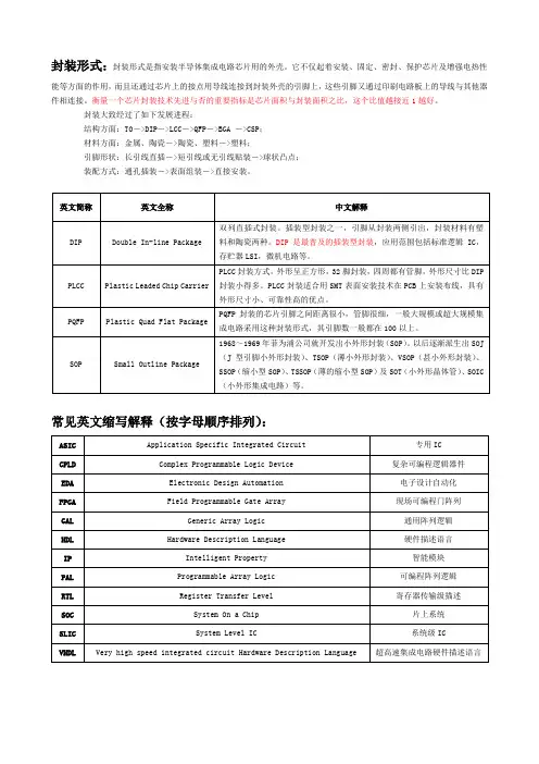
IC封装术语(中英文对照)1、SOW (Small Outline Package(Wide-Jype))宽体SOP。
部分半导体厂家采用的名称。
2、SOF(small Out-Line package)小外形封装。
表面贴装型封装之一,引脚从封装两侧引出呈海鸥翼状(L 字形)。
材料有塑料和陶瓷两种。
另外也叫SOL 和DFP。
SOP 除了用于存储器LSI 外,也广泛用于规模不太大的ASSP 等电路。
在输入输出端子不超过10~40 的领域,SOP 是普及最广的表面贴装封装。
引脚中心距1.27mm,引脚数从8~44。
另外,引脚中心距小于1.27mm 的SOP 也称为SSOP;装配高度不到1.27mm 的SOP 也称为TSOP(见SSOP、TSOP)。
还有一种带有散热片的SOP。
3、SONF(Small Out-Line Non-Fin)无散热片的SOP。
与通常的SOP 相同。
为了在功率IC 封装中表示无散热片的区别,有意增添了NF(non-fin)标记。
部分半导体厂家采用的名称(见SOP)。
4、SQL(Small Out-Line L-leaded package)按照JEDEC(美国联合电子设备工程委员会)标准对SOP 所采用的名称(见SOP)。
5、SOJ(Small Out-Line J-Leaded Package)J 形引脚小外型封装。
表面贴装型封装之一。
引脚从封装两侧引出向下呈J 字形,故此得名。
通常为塑料制品,多数用于DRAM 和SRAM 等存储器LSI 电路,但绝大部分是DRAM。
用SOJ封装的DRAM 器件很多都装配在SIMM 上。
引脚中心距1.27mm,引脚数从20 至40(见SIMM)。
6、SOIC(small out-line integrated circuit)SOP 的别称(见SOP)。
国外有许多半导体厂家采用此名称。
7、SOI(small out-line I-leaded package)I 形引脚小外型封装。
电子技术名词中英文对照本征半导体:intrinsic semiconductor掺杂半导体:doped semiconductorP型半导体:P-type semiconductorN型半导体:N-type semiconductor自由电子:free electron空穴:hole载流子:carriersPN结:PN junction扩散:diffusion漂移:drift二极管:diode硅二极管:silicon diode锗二极管:germanium diode阳极:anode阴极:cathode发光二极管:light-emitting diode (LED)光电二极管:photodiode稳压二极管:Zener diode晶体管(三极管):transistorPNP型晶体管:PNP transistorNPN型晶体管:NPN transistor发射极:emitter集电极:collector基极:base电流放大系数:current amplification coefficient场效应管:field-effect transistor (FET)P沟道:p-channelN沟道:n-channel结型场效应管:junction FET(JFET)金属氧化物半导体:metal-oxide semiconductor (MOS)耗尽型MOS场效应管:depletion mode MOSFET(D-MOSFET)增强型MOS场效应管:enhancement mode MOSFET(E-MOSFET)源极:source栅极:grid漏极:drain跨导:transconductance夹断电压:pinch-off voltage热敏电阻:thermistor开路:open短路:shorted。
【集成电路(IC)】电子专业术语英汉对照加注解电子专业英语术语★rchitecture(结构):可编程集成电路系列的通用逻辑结构。
★ASIC(Application Specific Integrated Circuit-专用集成电路):适合于某一单一用途的集成电路产品。
★ATE(Automatic Test EQUIPment-自动测试设备):能够自动测试组装电路板和用于莱迪思ISP 器件编程的设备。
★BGA(Ball Grid Array-球栅阵列):以球型引脚焊接工艺为特征的一类集成电路封装。
可以提高可加工性,减小尺寸和厚度,改善了噪声特性,提高了功耗管理特性。
★Boolean Equation(逻辑方程):基于逻辑代数的文本设计输入方法。
★Boundary Scan Test(边界扫描测试):板级测试的趋势。
为实现先进的技术所需要的多管脚器件提供了较低的测试和制造成本。
★Cell-Based PLD(基于单元的可编程逻辑器件):混合型可编程逻辑器件结构,将标准的复杂的可编程逻辑器件(CPLD)和特殊功能的模块组合到一块芯片上。
★CMOS(Complementary Metal Oxide Semiconductor-互补金属氧化物半导体):先进的集成电路★加工工艺技术,具有高集成、低成本、低能耗和高性能等特征。
CMOS 是现在高密度可编程逻辑器件(PLD)的理想工艺技术。
★CPLD(Complex Programmable Logic Device-复杂可编程逻辑器件):高密度的可编程逻辑器件,包含通过一个中央全局布线区连接的宏单元。
这种结构提供高速度和可预测的性能。
是实现高速逻辑的理想结构。
理想的可编程技术是E2CMOS?。
★Density (密度):表示集成在一个芯片上的逻辑数量,单位是门(gate)。
密度越高,门越多,也意味着越复杂。
★Design Simulation(设计仿真):明确一个设计是否与要求的功能和时序相一致的过程。
★E2CMOS?(Electrically Erasable CMOS-电子可擦除互补金属氧化物半导体):莱迪思专用工艺。
基于其具有继承性、可重复编程和可测试性等特点,因此是一种可编程逻辑器件(PLD)的理想工艺技术。
★EBR(Embedded BLOCk RAM-嵌入模块RAM):在ORCA 现场可编程门阵列(FPGA)中的RAM 单元,可配置成RAM、只读存储器(ROM)、先入先出(FIFO)、内容地址存储器(CAM)等。
★EDA(Electronic Design Automation-电子设计自动化):即通常所谓的电子线路辅助设计软件。
★EPIC (Editor for Programmable Integrated Circuit-可编程集成电路编辑器):一种包含在★ORCA Foundry 中的低级别的图型编辑器,可用于ORCA 设计中比特级的编辑。
★Explore Tool(探索工具):莱迪思的新创造,包括ispDS+HDL 综合优化逻辑适配器。
探索工具为用户提供了一个简单的图形化界面进行编译器的综合控制。
设计者只需要简单地点击鼠标,就可以管理编译器的设置,执行一个设计中的类似于多批处理的编译。
★Fmax:信号的最高频率。
芯片在每秒内产生逻辑功能的最多次数。
★FAE(Field Application Engineer-现场应用工程师):在现场为客户提供技术支持的工程师。
★Fabless:能够设计,销售,通过与硅片制造商联合以转包的方式实现硅片加工的一类半导体公司。
★Fitter(适配器):在将一个设计放置到目标可编程器件之前,用来优化和分割一个逻辑设计的软件。
★Foundry:硅片生产线,也称为fab。
FPGA(Field Programmable Gate Array-现场可编程门阵列):高密度PLD 包括通过分布式可编程阵列开关连接的小逻辑单元。
这种结构在性能和功能容量上会产生统计变化结果,但是可提供高寄存器数。
可编程性是通过典型的易失的SRAM 或反熔丝工艺一次可编程提供的。
★"Foundry" :一种用于ORCA 现场可编程门阵列(FPGA)和现场可编程单芯片系统(FPSC)的软件系统。
★FPGA(Field Programmable Gate Array-现场可编程门阵列):含有小逻辑单元的高密度PLD,这些逻辑单元通过一个分布式的阵列可编程开关而连接。
这种体系结构随着性能和功能容量不同而产生统计上的不同结果,但是提供的寄存器数量多。
其可编程性很典型地通过易失SRAM 或者一次性可编程的反熔丝来体现。
★FPSC(Field Programmable System-on-a-Chip-现场可编程单芯片系统):新一代可编程器件用于连接FPGA 门和嵌入的ASIC 宏单元,从而形成一芯片上系统的解决方案。
★GAL? (Generic Array Logic-通用阵列逻辑):由莱迪思半导体公司发明的低密度器件系统。
★Gate(门):最基本的逻辑元素,门数越多意味着密度越高。
★Gate Array(门阵列):通过逻辑单元阵列连接的集成电路。
由生产厂家定制,一般会导致非再生工程(NRE)消耗和一些设计冗余。
★GLB(Generic Logic BLOCk-通用逻辑块):莱迪思半导体的高密度ispPSI?器件的标准逻辑块。
每一个GLB 可实现包含输入、输出的大部分逻辑功能。
★GRP(Global Routing Pool-全局布线池):专有的连接结构。
能够使GLBs 的输出或I/O 单元输入与GLBs 的输入连接。
莱迪思的GRP 提供快速,可预测速度的完全连接。
★High Density PLD(高密度可编程逻辑器件):超过1000 门的PLD。
★I/O Cell(Input/Output Cell-输入/输出单元):从器件引脚接收输入信号或提供输出信号的逻辑单元。
★ISPTM(In-System Programmability-在系统可编程):由莱迪思首先推出,莱迪思ISP 产品可以在系统电路板上实现编程和重复编程。
ISP 产品给可编程逻辑器件带来了革命性的变化。
它极大地缩短了产品投放市场的时间和产品的成本。
还提供能够对在现场安装的系统进行更新的能力。
★ispATETM:完整的软件包使自动测试设备能够实现:1)利用莱迪思ISP 器件进行电路板测试和2)编程ISP 器件。
★ispVM EMBEDDEDTM:莱迪思半导体专用软件由C 源代码算法组成,用这些算法来执行控制编程莱迪思ISP 器件的所有功能。
代码可以被集成到用户系统中,允许经由板上的微处理器或者微控制器直接编程ISP 器件。
★ispDaisy Chain Download SOFtware (isp菊花链下载软件):莱迪思半导体专用器件下载包,提供同时对多个在电路板上的器件编程的功能。
★ispDSTM:莱迪思半导体专用基于Windows 的软件开发系统。
设计者可以通过简单的逻辑公式或莱迪思- HDL 开发电路,然后通过集成的功能仿真器检验电路的功能。
整个工具包提供一套从设计到实现的方便的、低成本和简单易用的工具。
★ispDS+TM:莱迪思半导体兼容第三方HDL综合的优化逻辑适配器,支持PC和工作站平台。
IspDS+ 集成了第三方CAE 软件的设计入口和使用莱迪思适配器进行验证,由此提供了一个功能强大、完整的开发解决方案。
第三方CAE 软件环境包括:Cadence,Date I/O-Synario,Exemplar Logic,ISDATA,Logical Devices,Mentor Graphics,OrCAD,Synopsys,Synplicity 和Viewlogic。
★isPGAL?:具有在系统可编程特性的GAL 器件★ispGDSTM:莱迪思半导体专用的ISP 开关矩阵被用于信号布线和DIP 开关替换。
★ispGDXTM:ISP 类数字交叉点系列的信号接口和布线器件。
★ispHDLTM:莱迪思开发系统,包括功能强大的VHDL 和Verilog HDL 语言和柔性的在系统可编程。
完整的系统包括:集成了Synario,Synplicity 和Viewlogic 的综合工具,提供莱迪思ispDS+ HDL 综合优化逻辑适配器。
★ispLSI?:莱迪思性能领先的CPLD 产品系列的名称。
世界上最快的高密度产品,提供非易失的,在系统可编程能力和非并行系统性能。
★ispPAC?:莱迪思唯一的可编程模拟电路系列的名称。
世界上第一个真正的可编程模拟产品,提供无与伦比的所见即所得(WYSIYG)逻辑设计结果。
★ispSTREAMTM:JEDEC 文件转化为位封装格式,节省原文件1/8 的存储空间。
★ispTATM:莱迪思静态时序分析器,是ispDS+ HDL 综合优化逻辑适配器的组成部分。
包括所有的功能。
使用方便,节省了大量时序分析的代价。
设计者可以通过时序分析器方便地获得任何莱迪思ISP 器件的引脚到引脚的时序细节。
通过一个展开清单格式方便地查看结果。
★ispVHDLTM:莱迪思开发系统。
包括功能强大的VHDL 语言和灵活的在系统可编程。
完整的系统工具包括Synopsys,Synplicity 和Viewlogic,加上ispDS+ HDL 综合优化逻辑适配器。
★ispVM System:莱迪思半导体第二代器件下载工具。
是基于能够提供多供应商的可编程支持的便携式虚拟机概念设计的。
提高了性能,增强了功能。
★JEDEC file(JEDEC 文件):用于对ispLSI 器件编程的工业标准模式信息。
★JTAG(Joint Test Action Group-联合测试行动组):一系列在主板加工过程中的对主板和芯片级进行功能验证的标准。
★Logic(逻辑):集成电路的三个基本组成部分之一:微处理器内存和逻辑。
逻辑是用来进行数据操作和控制功能的。
★Low Density PLD(低密度可编程逻辑器件):小于1000 门的PLD,也称作SPLD。
★LUT (Look-Up Table-查找表):一种在PFU 中的器件结构元素,用于组合逻辑和存储。
基本上是静态存储器(SRAM)单元。
★Macrocell(宏单元):逻辑单元组,包括基本的产品逻辑和附加的功能:如存储单元、通路控制、极性和反馈路径。
★MPI(MicroprocesSOr Interface-微处理器接口):ORCA 4 系列FPGA 的器件结构特征,使FPGA 作为随动或外围器件与PowerQUIC mP 接口。
★OLMC(Output Logic Macrocell-输出逻辑宏单元):D 触发器,在输入端具有一个异或门,每一个GLB 输出可以任意配置成组合或寄存器输出。