MC10H115M资料
- 格式:pdf
- 大小:152.56 KB
- 文档页数:6
© Semiconductor Components Industries, LLC, 2006February, 2006 − Rev. 71Publication Order Number:MC10H115/DMC10H115
Quad Line Receiver
DescriptionThe MC10H115 is a quad differential amplifier designed for use insensing differential signals over long lines. This 10H part is afunctional/ pinout duplication of the standard MECL 10K™ familypart, with 100% improvement in counting frequency and no increasein power supply current.The base bias supply (VBB) is made available at Pin 9 to make thedevice useful as a Schmitt trigger, or in other applications where astable reference voltage is necessary. Active current sources providethe MC10H115 with excellent common mode rejection. If anyamplifier in a package is not used, one input of that amplifier must beconnected to VBB (Pin 9) to prevent upsetting the current source biasnetwork.The MC10H115 is designed to be used in sensing differentialsignals over long lines. The bias supply (VBB) is made available tomake the device useful as a Schmitt trigger, or in other applicationswhere a stable reference voltage is necessary.Active current sources provide these receivers with excellentcommon−mode noise rejection. If any amplifier in a package is notused, one input of that amplifier must be connected to VBB to preventunbalancing the current source bias network.The MC10H115 does not have internal input pulldown resistors.This provides high impedance to the amplifier input and facilitatesdifferential connections.
Features•Propagation Delay, 1.0 ns Typical•Power Dissipation 110 mW Typ/Pkg (No Load)•Improved Noise Margin 150 mV (Over Operating Voltage andTemperature Range)•Voltage Compensated•MECL 10K Compatible
Applications•Low Level Receiver•Voltage Level Interface•Schmitt Trigger•Pb−Free Packages are Available*
*For additional information on our Pb−Free strategy and soldering details, pleasedownload the ON Semiconductor Soldering and Mounting TechniquesReference Manual, SOLDERRM/D.
CDIP−16L SUFFIXCASE 620AMARKING DIAGRAMS*
PDIP−16P SUFFIXCASE 648http://onsemi.com
*For additional marking information, refer to Application Note AND8002/D.
See detailed ordering and shipping information in the packagedimensions section on page 3 of this data sheet.ORDERING INFORMATIONSOEIAJ−16CASE 96616116
1MC10H115PAWLYYWWG116
MC10H115LAWLYYWW
A= Assembly LocationWL, L= Wafer LotYY, Y= YearWW, W= Work WeekG=
Pb−Free Package10H115ALYWG
PLLC−20FN SUFFIXCASE 77520110H115GAWLYYWW120元器件交易网www.cecb2b.comMC10H115
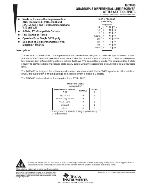
http://onsemi.com2Figure 1. Logic DiagramFigure 2. Pin AssignmentVCC1AoutBoutAinAinBinBinVEEVCC2DoutCoutDinDinCinCin
VBB1615141312111091234567
8254
367
141110
151213
9*VBB to be used to supply bias to the MC10H115 only andbypassed (when used) with 0.01 mF to 0.1 mF capacitorto ground (0 V). VBB can source < 1.0 mA.When input pin with bubble goes positive its respective output pin with bubble goes positive.
VBB*VCC1 = Pin 1VCC2 = Pin 16VEE = Pin 8Pin assignment is for Dual−in−Line Package.
Table 1. MAXIMUM RATINGSSymbolCharacteristicRatingUnit
VEEPower Supply (VCC = 0)−8.0 to 0Vdc
VIInput Voltage (VCC = 0)0 to VEEVdc
IoutOutput CurrentContinuousSurge50100mA
TAOperating Temperature Range0 to +75°C
TstgStorage Temperature RangePlasticCeramic−55 to +150−55 to +165°C°CMaximum ratings are those values beyond which device damage can occur. Maximum ratings applied to the device are individual stress limitvalues (not normal operating conditions) and are not valid simultaneously. If these limits are exceeded, device functional operation is not implied,damage may occur and reliability may be affected.
Table 2. ELECTRICAL CHARACTERISTICS (VEE = −5.2 V ±5%) (Note 2)0°25°75°
SymbolCharacteristicMinMaxMinMaxMinMaxUnit
IEPower Supply Current−29−26−29mA
IinHInput Current High−150−95−95mA
ICBOInput Leakage Current−1.5−1.0−1.0mA
VBBReference Voltage−1.38−1.27−1.35−1.25−1.31−1.19Vdc
VOHHigh Output Voltage−1.02−0.84−0.98−0.81−0.92−0.735Vdc
VOLLow Output Voltage−1.95−1.63−1.95−1.63−1.95−1.60Vdc
VIHHigh Input Voltage (Note 1)−1.17−0.84−1.13−0.81−1.07−0.735Vdc
VILLow Input Voltage (Note 1)−1.95−1.48−1.95−1.48−1.95−1.45Vdc
VCMRCommon ModeRange (Note 3)−−−2.85 to −0.8−−Vdc
VPPInput Sensitivity (Note 4)−−150 typ−−mVPP1.When VBB is used as the reference voltage.2.Each MECL 10H™ series circuit has been designed to meet the specifications shown in the test table, after thermal equilibrium has beenestablished. The circuit is in a test socket or mounted on a printed circuit board and transverse air flow greater than 500 linear fpm ismaintained. Outputs are terminated through a 50 W resistor to −2.0 V.3.Differential input not to exceed 1.0 Vdc.4.150 mVp−p differential input required to obtain full logic swing on output.元器件交易网www.cecb2b.com