MC100EP139资料
- 格式:pdf
- 大小:143.52 KB
- 文档页数:8
© Semiconductor Components Industries, LLC, 1999December, 1999 – Rev. 11Publication Order Number:MC100EP139/DMC100EP139
ProductPreview÷2/4,÷4/5/6ClockGenerationChip
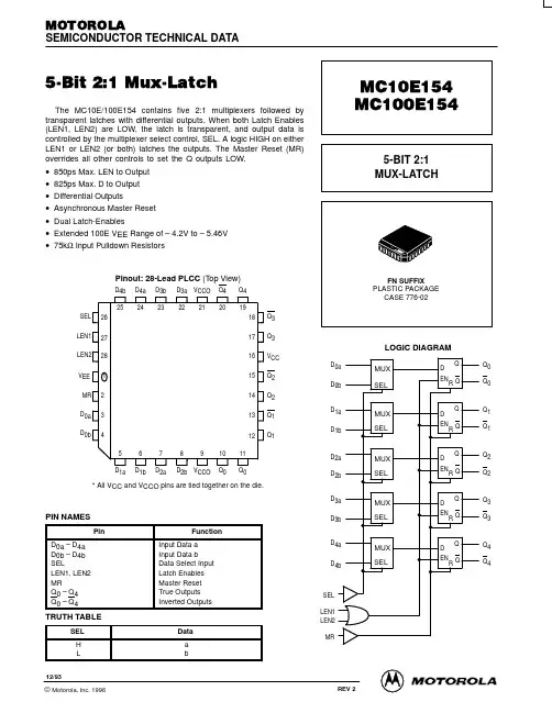
The MC100EP139 is a low skew ÷2/4, ÷4/5/6 clock generation chipdesigned explicitly for low skew clock generation applications. Theinternal dividers are synchronous to each other, therefore, the commonoutput edges are all precisely aligned. The device can be driven byeither a differential or single–ended ECL or, if positive power suppliesare used, LVPECL input signals. In addition, by using the VBB output,a sinusoidal source can be AC coupled into the device. If asingle–ended input is to be used, the VBB output should be connectedto the CLK input and bypassed to ground via a 0.01µF capacitor.The common enable (EN) is synchronous so that the internaldividers will only be enabled/disabled when the internal clock isalready in the LOW state. This avoids any chance of generating a runtclock pulse on the internal clock when the device is enabled/disabledas can happen with an asynchronous control. The internal enableflip–flop is clocked on the falling edge of the input clock, therefore, allassociated specification limits are referenced to the negative edge ofthe clock input.Upon startup, the internal flip–flops will attain a random state;therefore, for systems which utilize multiple EP139s, the master reset(MR) input must be asserted to ensure synchronization. For systemswhich only use one EP139, the MR pin need not be exercised as theinternal divider design ensures synchronization between the ÷2/4 andthe ÷4/5/6 outputs of a single device. All VCC and VEE pins must beexternally connected to power supply to guarantee proper operation.•50ps Output–to–Output Skew•PECL mode: 3.0V to 5.5V VCC with VEE = 0V•ECL mode: 0V VCC with VEE = –3.0V to –5.5V•Synchronous Enable/Disable•Master Reset for Synchronization of Multiple Chips•Q Output will default LOW with inputs open or at VEE•ESD Protection: >2KV HBM, >100V MM•VBB Output•New Differential Input Common Mode Range•Moisture Sensitivity Level 2For Additional Information, See Application Note AND8003/D•Flammability Rating: UL–94 code V–0 @ 1/8”, Oxygen Index 28 to 34•Transistor Count = 758 devices
This document contains information on a product under development. ON Semiconductorreserves the right to change or discontinue this product without notice.TSSOP–20DT SUFFIXCASE 948Ehttp://onsemi.com
DevicePackageShippingORDERING INFORMATION
MC100EP139DTTSSOP75 Units/RailMARKING DIAGRAM
MC100EP139DTR2TSSOP2500 Tape/ReelSO–20DW SUFFIXCASE 751D
MC100EP139DWSOIC38 Units/RailMC100EP139DWR2SOIC2500 Tape/Reel*For additional information, see Application Note AND8002/DKEP139ALYW
A= Assembly LocationL= Wafer LotY= YearW= Work WeekMC100EP139AWLYWW
A= Assembly LocationWL= Wafer LotYY= YearWW= Work Week元器件交易网www.cecb2b.comMC100EP139
http://onsemi.com2CLK
Figure 1. 20–Lead SOIC (Top View)CLKMRVCC17181615141312
4356789Q011
10Q1Q1Q2Q2Q3Q3VEE
EN1920
21VCCQ0
VBBVCCDIVSELb0
DIVSELb1DIVSELa
Z = Low–to–High TransitionZZ = High–to–Low TransitionCLKENFUNCTIONZZZXLHXDivideHold Q0:3Reset Q0:3FUNCTION TABLESMRLLH
DIVSELaQ0:1 OUTPUTS01Divide by 2Divide by 4DIVSELb0Q2:3 OUTPUTS0101Divide by 4Divide by 6Divide by 5Divide by 5DIVSELb10011Warning: All VCC and VEE pins must be externally connectedto Power Supply to guarantee proper operation.
PIN DESCRIPTIONPINCLK, CLKENECL Sync EnableFUNCTIONECL Diff Clock Inputs
MRVBBECL Reference OutputECL Master ResetQ0, Q1, Q0, Q1Q2, Q3, Q2, Q3ECL Diff ÷4/5/6 OutputsECL Diff ÷2/4 OutputsDIVSELaDIVSELb0ECL Freq. Select Input B4/5/6ECL Freq. Select Input B2/4
DIVSELb1ECL Freq. Select Input B4/5/6VCCVEEECL Negative, 0 SupplyECL Positive Supply
CLKCLK
EN
MRDIVSELb1÷2/4Q0Q0Q1Q1
÷4/5/6Q2Q2Q3Q3Figure 2. Logic DiagramRRDIVSELa
DIVSELb0元器件交易网www.cecb2b.comMC100EP139
http://onsemi.com3CLKQ (÷2)Q (÷4)Q (÷5)
Figure 3. Timing DiagramQ (÷6)
Figure 4. Timing DiagramCLK
RESET
Q (÷n)tRR
MAXIMUM RATINGS*SymbolParameterValueUnitVEEPower Supply (VCC = 0V)–6.0 to 0VDCVCCPower Supply (VEE = 0V)6.0 to 0VDCVIInput Voltage (VCC = 0V, VI not more negative than VEE)–6.0 to 0VDCVIInput Voltage (VEE = 0V, VI not more positive than VCC)6.0 to 0VDCIoutOutput CurrentContinuousSurge50100mA
IBBVBB Sink/Source Current{±0.5mATAOperating Temperature Range–40 to +85°CTstgStorage Temperature–65 to +150°CθJA (DT Suffix)Thermal Resistance (Junction–to–Ambient)Still Air500lfpm140100°C/W
θJC (DT Suffix)Thermal Resistance (Junction–to–Case)23 to 41 ± 5%°C/WθJA (DW Suffix)Thermal Resistance (Junction–to–Ambient)Still Air500lfpm9060°C/W
θJC (DW Suffix)Thermal Resistance (Junction–to–Case)33 to 35 ± 5%°C/WTsolSolder Temperature (<2 to 3 Seconds: 245°C desired)265°C* Maximum Ratings are those values beyond which damage to the device may occur.{ Use for inputs of same package only.元器件交易网www.cecb2b.com