Thin-film adhesion
- 格式:pdf
- 大小:1.19 MB
- 文档页数:9

光伏行业英文词汇(共13页)--本页仅作为文档封面,使用时请直接删除即可----内页可以根据需求调整合适字体及大小--太阳电池 solar cell通常是指将太阳光能直接转换成电能的一种器件。
硅太阳电池silicon solar cell硅太阳电池是以硅为基体材料的太阳电池。
单晶硅太阳电池single crystalline silicon solar cell单晶硅太阳电池是以单晶硅为基体材料的太阳电池。
非晶硅太阳电池(a—si太阳电池)amorphous silicon solar cell用非晶硅材料及其合金制造的太阳电池称为非晶硅太阳电池,亦称无定形硅太阳电池,简称a—si太阳电池。
多晶硅太阳电池polycrystalline silicon solar cell多晶硅太阳电池是以多晶硅为基体材料的太阳电池。
聚光太阳电池组件photovoltaic concentrator module系指组成聚光太阳电池,方阵的中间组合体,由聚光器、太阳电池、散热器、互连引线和壳体等组成。
电池温度cell temperature系指太阳电池中P-n结的温度。
太阳电池组件表面温度solar cell module surface temperature系指太阳电池组件背表面的温度。
大气质量(AM)Air Mass (AM)直射阳光光束透过大气层所通过的路程,以直射太阳光束从天顶到达海平面所通过的路程的倍数来表示。
太阳高度角 solar 太阳高度角 solar elevation angle太阳光线与观测点处水平面的夹角,称为该观测点的太阳高度角。
辐照度 irradiance系指照射到单位表面积上的辐射功率(W/m2)。
总辐照(总的太阳辐照)total irradiation (total insolation)在一段规定的时间内,(根据具体情况而定为每小时,每天、每周、每月、每年)照射到某个倾斜表面的单位面积上的太阳辐照。
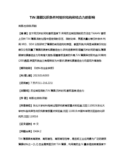
TiN薄膜沉积条件对组织结构和结合力的影响肖娜;杜菲菲;邢韵【摘要】在不同沉积时间和基板温度下,采用反应磁控溅射的方法在Ti6Al4V基板上沉积TiN薄膜,溅射过程中固定溅射总压、溅射功率、氮氩流量比等沉积条件.利用XRD、SEM分别研究了薄膜的微观结构和表面、截面形貌,利用显微硬度仪和划痕仪分别测量了薄膜的硬度和膜基结合力.研究结果表明:随着沉积时间的增加,薄膜硬度和膜基结合力均有增大趋势;随着基板温度的升高,TiN薄膜择优取向由(lll)转向(200)晶面,表面形貌由三角锥转变为片层状,硬度和膜基结合力均呈现升高趋势.【期刊名称】《材料与冶金学报》【年(卷),期】2015(014)003【总页数】7页(P211-216,221)【关键词】反应磁控溅射;TiN薄膜;沉积时间;基板温度;结合力【作者】肖娜;杜菲菲;邢韵【作者单位】东北大学材料电磁过程研究教育部重点实验室,沈阳110819;东北大学材料各向异性与织构教育部重点实验室,沈阳110819;中国科学院沈阳自动化研究所,沈阳110016【正文语种】中文【中图分类】O484.2TiN薄膜具有高硬度、高耐磨性、高耐腐蚀性等,是目前工业应用最为广泛的硬质薄膜材料之一[1,2].在金属表面沉积TiN薄膜,利用高的含N量来维持其高强度不仅保留了金属本身的强度和韧性,而且在其表面又增加了陶瓷材料的高硬度、低磨损和耐腐蚀性.在金属表面沉积TiN薄膜可以采用多弧离子镀、磁控溅射、离子束辅助沉积、反应等离子喷涂等方法[3].在制备过程中发现溅射总压的大小会直接影响TiN薄膜的颜色[4],氮气、氩气的流量对TiN膜层颜色、结构、表面形貌、导电性等也存在不同程度的影响[5~8]. 反应磁控溅射的沉积条件不仅仅包含溅射气压,气体流量,还包含沉积时间、基板温度等,本文主要从沉积时间、基板温度两个角度考察沉积条件对TiN薄膜组织结构、硬度、结合力等的影响.本文采用反应磁控溅射的方法,利用JZCK-440S高真空镀膜设备,在Ti6Al4V基板上沉积一系列TiN薄膜.实验过程中固定氮气和氩气的流量比、溅射气压和溅射功率,分别改变沉积时间、基板温度进行两组实验,具体工艺见表1.利用Smartlab-X射线衍射仪分析了薄膜的晶体结构、 OLS-3100激光共聚焦显微镜对薄膜划痕形貌进行了观察、JSM-7001F场发射扫描电镜观察薄膜的微观组织,使用Wolpert-401MVDTM数显显微硬度仪测量薄膜的硬度、WS-2005涂层附着力自动划痕仪测量膜/基结合力.划痕仪使用参数:加载载荷为100 N、加载速率为100 N/min、划痕长度为4 mm.图1为不同沉积时间制备TiN薄膜样品的X射线衍射谱图,由图1(a)可看到(111)、(200)、(220)、(311)和(222)等TiN的衍射峰.从图(b)可以看出,随着沉积时间的增加,基体α-Ti的衍射峰逐渐变弱;而TiN薄膜衍射峰峰强增大,且同时存在(111)和(200)两种特征衍射峰. 图2为不同沉积时间TiN薄膜的表面形貌,可以看出随着沉积时间的增加,薄膜的晶粒尺寸也增大.图3为不同沉积时间下TiN薄膜的截面形貌,随着沉积时间从1 h增加到6 h,薄膜的厚度从0.64 μm增加到3.6 μm.当沉积时间为1~2 h时,薄膜没有表现出柱状晶,直到沉积时间增加到4 h以上,薄膜生长表现出明显的柱状晶.对比沉积时间4 h和6 h的截面形貌发现,沉积时间为4 h的截面形貌可以观察到薄膜在近表面处并不是以柱状晶生长而是一层致密的厚膜,沉积时间为6 h时,薄膜完全以柱状晶方式生长,晶粒尺寸较大.图4为不同沉积时间TiN薄膜的硬度,随着沉积时间的增加TiN薄膜的硬度呈线性增加的趋势.沉积时间为1~2 h时,薄膜的厚度较小,致密度差,同时硬度受到基体硬度的影响(基体硬度为368 HV),所以硬度只有600~800 HV左右.随着时间的增加,厚度增大,硬度值也随之增大.当沉积时间为4 h时,硬度值增加到 1 360.3 HV.沉积时间为 6 h时,硬度值达到了2 089 HV,已经达到了TiN块体的硬度值[9].这个趋势与Hall-Petch公式(H=H0+k/λ1/2)相符合.图5是不同沉积时间不同薄膜样品的划痕形貌,白框区域为薄膜失效区,虚线所对应载荷值为薄膜开始剥落的临界值,即认定为薄膜与基体的结合力[10].图5(a)是沉积时间为1 h薄膜的临界载荷,观察划痕形貌发现在28 N附近薄膜开始剥落(即虚线位置处)由此判断薄膜的临界载荷为28 N,即薄膜与基体的结合力为28 N.图5(b)是沉积时间为2 h薄膜的临界载荷,薄膜在32 N后开始出现严重崩落现象,白色区域内可以看到典型的周边剥落现象[11,12],结合力为32 N.图5(c)是沉积时间为4 h薄膜的临界载荷,载荷加载到48 N,薄膜出现大面积连续剥落,白色区域内可以看出薄膜在基体“暴露”前划痕周边并没有薄膜崩落,为典型的屈曲剥落现象,结合力为 48 N.图5(d)是沉积时间为6 h薄膜的临界载荷,随着载荷的施加并未发生界面裂纹扩展,为典型的屈曲剥落现象,结合力是62 N.图6为不同沉积时间TiN薄膜与基体结合力的变化曲线.随着沉积时间的增加结合力呈线性增加,当沉积时间为6 h时基膜结合力达到了62 N.这与薄膜硬度随沉积时间的变化规律相同,因为硬度较高时,薄膜在载荷的作用下不易发生塑性变形,延缓了压头压入薄膜所造成的过早破裂和剥落,提高了基膜结合力.图7为不同基板温度TiN薄膜的XRD谱图,从(a)图可以看出不同基板温度下沉积的薄膜均出现(111)、(200)、(220)、(311)和(222)TiN的特征衍射峰.从(b)图可以看出,室温条件下薄膜的取向以(111)晶面为主,100℃时(111)和(200)晶面同时存在,当温度升到200℃以上时,(111)织构减少(200)织构增多.对于TiN结构,(200)晶面为其表面能最低晶面,(111)晶面为其应变能最小晶面[13].基板温度低时,薄膜应力较大,沿应变能最小的(111)晶面择优生长,随着温度的升高,应力得到释放,择优取向转向表面能最低的(200)晶面,这与张金林等得到的结果一致[14]. 图8是不同基板温度TiN薄膜的表面形貌.薄膜在室温下表面是明显的三角锥形结构;温度为100 ℃和200 ℃时,薄膜的表面形貌部分呈三角锥形、部分呈片状结构;随着温度升高到340 ℃时,薄膜呈片状结构.结合图7的XRD结果,低温时,薄膜择优取向为(111)晶面、形貌呈三角锥形状;随着温度的升高薄膜择优取向有从(111)晶面转向(200)晶面的趋势、同时形貌也呈现出三角锥和片状共存状态;温度达到340 ℃时,薄膜(200)取向更为明显,形貌也变成片状结构.这一结果说明,TiN薄膜取向和形貌之间存在一定的关联. 图9为不同基板温度下TiN薄膜的硬度,室温时薄膜的硬度为 1 048.5 HV,室温到200 ℃之间的硬度值变化不大,当温度增加到340 ℃时,薄膜的硬度为 1 360.3 HV,总体来说薄膜的硬度随着基板温度的增加而上升.可能是由于基体温度的增加,吸附原子的迁移率随之增加,因而提高了Ti和N的结合率和薄膜韧性,阻止了载荷压入过程中微裂纹的传播和增殖,最终导致薄膜硬度的提高.图10是不同基板温度TiN薄膜样品的划痕形貌.图10(a)是基板温度为25 ℃时薄膜的临界载荷,当载荷加载到20 N左右时薄膜开始出现周边剥落现象,结合力为19 N.图10(b)是基板温度为100 ℃薄膜的临界载荷,整条划痕周边均有薄膜严重崩落的现象,10 N以下薄膜就表现出典型的压缩剥落形貌,剥离区域面积大,边缘呈弧形剥落,该薄膜与基体的结合力为9 N.图10(c)是基板温度为200 ℃薄膜的临界载荷,薄膜在基体“暴露”前划痕周边并没有出现崩落现象,直到41 N 左右时才出现大面积连续剥落,结合力为41 N.图10(d)是基板温度为340℃薄膜临界载荷,直到加载载荷为49 N时才出现大面积连续剥落,判定薄膜的结合力为49 N.图11为不同基板温度下TiN薄膜与基体结合力的变化曲线,其中结合力出现先减小后增大的趋势,可能是因为薄膜内压应力与热应力竞争导致的[17].当基板温度为室温时,薄膜表面主要存在压应力,膜基结合力相对较高.但温度增加到100~200 ℃时,热应力大于压应力,导致薄膜易开裂,所以结合力降低.当温度达到340 ℃时,由于Ti原子的能量较高,所以沉积在薄膜表面的压应力大于热应力,导致结合力又出现上升趋势.(1)随着沉积时间从1 h增加至6 h,薄膜厚度由600 nm增加至3 600 nm,薄膜的硬度从636.5 HV增加到2089 HV,膜基结合力也由32 N增加到43 N. (2)随着基板温度的上升,平行薄膜表面的晶面由(111)向(200)转变,表面形貌由三角锥状向片状转变;当温度为由25 ℃增加到340 ℃时,膜基结合力从19 N增加到49 N,硬度从1 048 HV 增大到1 360 HV.【相关文献】[1]宋贵宏, 杜昊, 贺春林. 硬质与超硬涂层:结构, 性能, 制备与表征. 北京:化学工业出版社, 2007. (Song G H , Du H, He C L. Hard and superhard coatings: structure, performance, preparation and characterization. Beijing:Chemical Industry Press, 2007.)[2]Lin N, Huang X, Zhang X,etal. In vitro assessments on bacterial adhesion and corrosion performance of TiN coating on Ti6Al4V titanium alloy synthesized by multi-arc ion plating. Applied Surface Science, 2012, 258(18): 7047-7051.[3]晏鲜梅, 熊惟皓. TiN硬质薄膜的制备方法. 材料导报, 2006, 5(20): 236-238.(Yan X M, Xiong W H. Preparation methods of TiN hard films. Materials Review, 2006,5(20): 236-238.)[4]杜菲菲. 反应溅射TiN梯度薄膜及其力学性能研究. 沈阳:东北大学, 2014.(Du F F. Preparation and me chemical properties of TiN compositional gradient films byreactive sputtering. Shenyang:Northeastern University, 2014.)[5]吕长东, 黄美东, 刘野, 等. 氮气流量对磁控溅射TiN膜层色泽的影响. 电镀与精饰, 2013, 3(35): 5-12.(Lv C D, Huang M D, Liu Y,etal. Regulation of the chromaticity of sputtered TiN films by changing nitrogen flow. Plating and Finishing, 2013, 3(35): 5-12.)[6]田颖萍, 范洪远, 成靖文. 氮氩流量比对磁控溅射TiN薄膜生长织构的影响. 表面技术, 2012,3(41):19-25.(Tian Y P, Fan H Y, Cheng J W. Effect of N2/Ar flow ratio orientation of TiN thin films. Surface Technology, 2012, 3(41):19-25.)[7]刘倩, 刘莹, 朱秀榕, 等. 氩气与氮气流量比对磁控溅射法制备TiN薄膜的影响. 机械工程材料, 2009, 3(33):8-11.(Liu Q, Liu Y, Zhu X R,etal. Influence of Ar and N2folw ratio on TiN thin films prepared by magnetron sputtering. Material of Mechanical Engineering, 2009, 3(33):8-11.)[8]雒向东. 不同氮气流量比反应溅射TiN薄膜的表面形貌分形特征. 量子电子学报, 2008, 5(25):346-350.(Luo X D. Fractal surface of TiN thin films sputtered at different N2flow ratio. Chinese Journal of Quantum Electronics, 2008, 5(25):346-350.)[9]Gen Q Y, Da Z W, Xiang H L,etal. Formation of nanocrystalline TiN films by ion-beam-enhanced deposition. Surface and Coatings Technology, 1994, 65(1): 214-218.[10]Mittal K L. Adhesion measurement of thin film. Electrocomponetnt Science and Technology, 1976, 3:21-42.[11]江范清. 划痕法评价氮化钛薄膜结合力研究. 成都:西南交通大学, 2012.(Jiang F Q. Adhesion measurement of titanium nitride coatings using the scratch test . Chengdu:Southwest Jiaotong University, 2012.)[12]肖娜, 杜菲菲, 杨波. 调制比对TiN/Ti 多层膜结构和力学性能的影响. 材料与冶金学报,2014,4(13): 276-279.(Xiao N, Du F F, Yang B. The effect of modulation ratio on structure and mechanical properties of TiN/Ti multilayer films. Journal of Materials and Metallurgy, 2014,4(13): 276-279.)[13]Patsalas P, Charitidis C, Logothetidis S. The effect of substrate temperature and biasing on the mechanical properties and structure of sputtered titanium nitride thin films. Surface and Coating Technology, 2001, 125(1/2/3):335-340.[14]张金林, 贺春林, 王建明, 等.基体温度对磁控溅射TiN薄膜结构与力学性能的影响. 沈阳大学学报(自然科学版), 2012,4(24): 23-27.(Zhang J L, He C L, Wang J M,etal. Effect of substrate temperature on microstructure and mechanical properties of magnetron sputtered TiN thin films. Journal of Shenyang University (Natural Science), 2012,4(24): 23-27.)[15]Zhang L, Yang H, Pang X,etal. Microstructure, residual stress, and fracture of sputtered TiN films. Surface and Coatings Technology, 2013, 224: 120-125.[16]Ljungcrantz H, Hultman L, Sundgren J E,etal. Residual stresses and fracture properties of magnetron sputtered Ti films on Si microelements. Journal of Vacuum Science & Technology A, 1993, 11(3): 543-553.[17]Hoang N H, McKenzie D R, McFall W D,etal. Properties of TiN films deposited at low temperature in a new plasma-based deposition system. Journal of Applied Physics, 1996, 80(11): 6279-6285.。

离子注入技术在半导体制造中的应用与研究半导体技术已经成为当今社会的支撑之一,而离子注入技术在半导体制造中起着非常重要的作用。
离子注入技术可以将精确的化学剂量注入到半导体材料内部,从而改变材料性质。
本文将讨论离子注入技术的原理、应用和研究。
原理离子注入技术利用电子轰击和加速反应,在细小的半导体材料表面上注入离子。
这种注入离子是一种精确的过程,具有高重复性和高可控性,可以在不同的半导体材料间产生特定的效果,如少子或多子注入。
此外,离子注入技术还可以将材料引入到材料中,产生瞬间的热反应,从而改变材料的性质。
这样的方法使得目标区域仅受到活性剂的影响,其它区域则不受到任何影响。
应用离子注入技术在半导体制造中应用广泛,作为半导体製造技术的一种重要手段,其应用主要体现在以下几个方面:1. Ion implantationIon implantation is a widely used method in semiconductor manufacturing. In this process, ions of a particular element are implanted into the surface of a semiconductor. This method can be used to increase carrier densities, tailoring dopant profiles, modify electrical and mechanical properties of semiconductors.2. Thin film growthIon implantation is an effective way to prepare thin films. During the process of ion implantation, the implanted ions are dispersed within a material and form small nuclei. These seed nuclei then grow into thin films, which can have various properties. Theseattributes include very high purity, controllable crystal structure, and extremely smooth surfaces.3. Surface modificationThe surface of the semiconductor material can be modified by ion implantation, such as enhancing the performance of MOSFET devices, reducing the impact of plasma damage during etching or deposition, and improving the adhesion of materials.研究离子注入技术的研究已经从单晶到多晶、从二维到三维,甚至实现了多种离子的复合注入。

2929 BondplyMulti-Layer Board Processing GuidelinesMATERIAL DESCRIPTION: 2929 bondply is an unreinforced, hydrocarbon based thin film adhesive system intended for use in high performance, high reliability multi-layer constructions.A low dielectric constant (2.9) and loss tangent (<0.003) at microwave frequencies makes it ideal for bonding multi-layer boards (MLB’s) made using PTFE composite materials such as RT/duroid® 6000 and RO3000® series laminates, filled hydro-carbon r esin c omposites s uch a s R O4000® c ores, a nd s pecialty t hin core laminates. The proprietary cross-linking resin system makes this thin film adhesive system compatible with sequential bond processing while controlled flow characteristics offer excellent blind via fill capability and potentially predictable cutback ratios for designs requiring blind and/or buried cavities. 2929 bondply is compatible with traditional flat press and autoclave bonding. The film is currently available in 0.0015”, 0.002”, and 0.003” thick sheets. Individual sheets can be stacked to yield thicker adhesive layers. The unreinforced thin film can be tack bonded to inner-layers to ease simultaneous machining of cut-outs through core and adhesive layers and to facilitate formation of vias using conductive pastes. An easy to release carrier film protects the adhesive layer from contamination during machining, screening of conductive pastes, and MLB booking. These processing guidelines offer current “best practice” procedures and parameters for bonding MLB’s using 2929 bondply. The recommendations will be updated as additional information becomes available. A Rogers’ Technical Service Engineer (TSE) should be consulted for our latest information. All first-time users are urged to contact a Rogers’ TSE, Sales Engineer (SE), or Applications Development Manager (ADM) for evaluation/ demonstration s amples a nd s pecial h andling i nstructions. A v ideo showing the recommended technique for laying up a multilayer using 2929 Bondply can be viewed in the video section on the Rogers Technology Support Hub: /techub. STORAGE: Materials should be stored between 10 to 30°C (50 to 80°F) and relative humidity less than 60%. The uncured material should be shielded from long-term exposures to UV light. 2929 bondply s hould b e u sed w ithin s ix m onths o f t he d ate o f s hipment.DESIGN CONSIDERATIONS: The post-bond thickness of 2929 bondply can be predicted using the following formula. It should be noted that copper distribution, planarity of platens and caul plates, layer count, compressible padding, etc… will effect the final thickness and uniformity thereof. The following calculation can be used as a starting point to predict post-bond core:core spacing, but fine tuning based upon actual thickness measurements is recommended.Core: core spacing = 2929 + (Side A Cu thk X retained Cu) + (Side B Cu thk X retained Cu) where:Core: core spacing is distance between etched core surfaceson opposing (A & B) sides of 2929 bondply. The distance is measured from the base of copper features.2929 is pre-press thickness of 2929 adhesive.Side A and Side B Cu thickness is the thickness of the copper layers on the A and B side of the 2929 bondply. Typically, 0.5ED would be 0.0007” while 1ED would be 0.0014”.Retained Cu is the percent of copper remaining on surfaceA andB after inner-layer preparation divided by 100. A solid copper plane would be 100%/100 = 1.0.Example:2929 thickness = 0.004”Side A Cu thick = 0.0007” (0.5E)Side B Cu thick = 0.0014” (1E)Side A retained Cu = 0.25 (25%/100)Side B retained Cu = 0.5 (50%/100)Core: core spacing =0.004” + (0.0007 X 0.25) + (0.0014 X 0.5) = 0.0049”Note: Cu:Cu spacing would be0.0049” – (0.0007” + 0.0014”) = 0.0028”FORMATION OF TOOLING HOLES: Tooling holes can be punched or drilled as single sheets or in stacks of multiple sheets. The maximum recommended stack height for punching holes is ten sheets. The maximum recommended stack height for drilling holes is 25 sheets providing a new drill and proper parameters are used.For either hole formation technique, the 2929 sheets should be stacked between layers of pressed phenolic entry material with the PET side on top. A release sheet should be placed between the phenolic sheet and the bottom layer of 2929 to avoid welding the adhesive to the exit material during formation of the tooling holes. The white tag stock paper used to package 2929 for shipment can be used as the release layer.Tooling holes can be punched as standard. Holes should be drilled using 200 SFM and a 0.0015”/” infeed rate. The default parameters for all drill diameters greater than 0.060” are 20 KRPM spindle speed and 25 IPM infeed. INNER LAYER PREPARATION: Innerlayer metal surfaces should be oxide treated to promote mechanical adhesion. A wide range of oxide alternatives and some reduced black or brown oxides have been used successfully with 2929 Bondply. The thermal capabilites of a given oxide treatment must be understood in order to select the appropriate lamination temperature.Please refer to the specific laminate manufacturers’ data sheets and processing guidelines for any recommended treatment of the etched dielectric surfaces and also to insure the laminates can tolerate the lamination temperature required for 2929 Bondply. MULTILAY ER LAY UP (Reference 2929 instructional video noted on page 1): The uncured adhesive layer is fragile. The release sheet facilitates handling, serves as a protective barrier against contamination, and should not be removed until after the adhesive layer has been punched, machined (cavity designs), and positioned onto the inner-layer surface. Once positioned onto the inner-layer surface, the carrier film should be carefully peeled beginning in one corner and peeling toward the diagonal corner. The preferred method of initiating the separation process involves bending one corner of the adhesive over until the PET carrier is in contact with itself. Pressing on the bend will snap the adhesive layer. The PET carrier can be slid toward the opposing corner while maintaining a slight downward pressure. The free hand should be used to hold down the adhesive layer during removal of the release liner. Special care may be required to avoid tearing of the adhesive layer near tooling holes and cut-outs. Pre-releasing and replacing the PET layer may prove helpful before machining cut-outs or when booking very thin (0.0015”) adhesive layers.Handling, especially of thin (<0.002” thick) layers, can be facilitated through the use of tack bonding. Tack bond is possible using a hot roll laminator at 125°C (275°F), 6” per minute feed rate, and 30 PSI. Tack bonding is also possible at 110°C (230°F) providing the feed rate is slowed to 2” per minute feed rate.Tack bonding can be accomplished using a vacuum lamination system. Parameters would include a 60-90 second dwell with bondline temperatures between 115 to 140°C (240 to 285°F). When possible, tooling holes should be formed after the tack bonding process. When properly applied, the tack bond should remain intact for 2-4 days and the adhesive layer should remain fully functional. Note: As is true with many bonding materials,the use of compressible padding placed internal to the tooling plates is recommended to improve pressure uniformity across the multilayer book. When selecting a press pad material, it is important to insure the material is properly rate for the selected bonding temperature. In addition, some designs may rquire additional conformance. In those cases, the use of skived PTFE or similar products have been used successfully between the multilayer panel and the stainless steel separators plates.MLB BONDING CYCLE: The press cycle should include a 2.5°C - 4.0°C/min (4.5°F - 7.0°F/min) ramp rate from room temperature to 245-250°C (473 to 482°F) and a 90-120 minute dwell at 245-250°C.NOTE: 2929 bondply can be bonded at lower temperatures if required t o c ompensate f or l ess t hermally r obust o xide t reatements.However, the absolute minimum product temperature must be above 224°C (435°F). Dwell time should be 120 minutes when cure temperature is less than 245-250°C (473 to 482°F). The recommended applied pressure for the entire cycle is 400 PSI, although pressure can be increased or decreased through evaluation to control flow of the resin/filler system. Vacuum assistance is preferred, but not required. Cooling can be accomplished in the hot press or after a transfer to a cold press for an accelerated rate of cooling. 2929 bondply is also compatible with a utoclave b onding u sing t he t hermal p rofile d escribed a bove.The information in this process guide is intended to assist you in designing and fabricating PWB’s with Rogers’ circuit materials. It is not intended to and does not create any warranties express or implied, including any warranty of merchantability or fitness for a particular purpose or that the results shown on this data sheet will be achieved by a user for a particular purpose. The user should determine the suitability of Rogers’ circuit materials for each application.Prolonged exposure in an oxidative environment may cause changes to the dielectric properties of hydrocarbon based materials. The rate of change increases at higher temperatures and is highly dependent on the circuit design. Although Rogers’ high frequency materials have been used successfully in innumerable applications and reports of oxidation resulting in performance problems are extremely rare, Rogers recommends that the customer evaluate each material and design combination to determine fitness for use over the entire life of the end product.These commodities, technology and software are exported from the United States in accordance with the Export Administration regulations. Diversion contrary to U.S. law prohibited.RT/duroid, RO4000, RO3000 and the Rogers’ logo are trademarks of Rogers Corporation or one of its subsidiaries.© 2021 Rogers Corporation, Printed in U.S.A, All rights reserved.POST-MLB BOND PROCESSING: With minor exceptions,bonded MLB’s should be processed using procedures and parameters associated with the core layers. Thin sub-assemblies should be handled carefully after bonding to avoid excessive bending. 2929 can be desmeared chemically or using plasma. A plasma cycle is provided below. The adhesive system does not require special sodium or plasma wettability treatments prior to plating, but 2929 is compatible with these processes should they be required for the core layers.Plasma Desmear CycleFrequency: 40 KHz Voltage: 500-600VPower: 4000-5000Watts Pre-Heat to 60°C using:Gases: 90% O2, 10% N2Pressure: 250mTORRDesmear using:Gases: 75% O2, 15% CF4, 10% N2Pressure 250 mTORR Time 10-15 minutes。
湖南大学硕士学位论文磁控反应溅射制备AlN薄膜及其性能研究姓名:刘新胜申请学位级别:硕士专业:材料物理指导教师:周灵平20070401硕士学位论文摘 要 AlN薄膜具有一系列独特的优良物理化学性质,在电学、光学、声学和力学等方面有广阔的应用前景。
尤其是AlN具有热导率高、电阻率高、击穿场强大、介电系数小、热膨胀系数与GaN、GaAs等常用半导体材料匹配这些特性,使其被广泛用作微电子和功率器件的基板、封装、介质隔离材料。
本研究工作采用MIS800型多功能离子束磁控溅射复合镀膜设备,分别在45钢、硅、钼衬底上制备出了高质量的AlN薄膜。
首先用XRD和SEM测试手段对沉积在45钢衬底上的AlN薄膜的结晶性能和组织结构进行了表征。
结果发现,衬底温度、氮气浓度和工作气压对AIN薄膜的结晶性能和组织结构有很大的影响。
通过引入AlN缓冲层,使薄膜的择优取向由原本的(100)晶面向(002)晶面演变;并且使薄膜的生长模式从岛状生长向层状生长过渡,从而增加了薄膜致密度,有效的提高了薄膜的结晶质量,为生长高质量的AIN薄膜提供了实验依据。
其次,用划痕测试仪对各个衬底上薄膜的粘结强度进行表征,结果表明,薄膜与基体界面处的结合状态是影响AlN薄膜的粘结强度的关键因素。
一系列的对比实验后发现,低能离子束清洗衬底表面、引入界面过渡层、对不同的衬底采用不同工艺都可以有效提高AlN薄膜的粘结强度。
AlN薄膜的制备方法和工艺对薄膜的组织结构和应力等产生较大的影响,采用双靶磁控溅射共沉积能有效改善薄膜的粘结性能,衬底温度和工作气压对双靶磁控溅射共沉积AlN薄膜粘结强度有一定影响。
最后,用超高电阻测试仪和绝缘耐压仪对薄膜的电学性能进行了测试,AlN 薄膜的电阻率高达6.4×10¹³Om,击穿场强高达1.32MV/cm,薄膜中的Al/N比和薄膜结晶质量是影响AlN薄膜电学性能的主要因素。
关键词:AlN薄膜;磁控溅射;结晶质量;粘结强度;电阻率;击穿场强 反应磁控溅射AlN薄膜制备及性能研究AbstractWurtzite Aluminum nitride (AlN) belongs to III–V semiconductor compounds with a hexagonal wurtzite crystal structure. Because of its high thermal conductivity, chemical stability, high hardness, high acoustic velocity, large electromechanical coupling coefficient and a wide band gap, AlN thin films have received great interest as a promising candidate electronic material for thermal dissipation, dielectric and passivation layers, surface acoustic wave (SAW) devices and photoelectric devices.In this paper, high quality AlN thin films were deposited on the 45 steel, Si and Mo substrates, respectively, by MIS800 ion beam sputtering and magnetron sputtering techniques simultaneously.Firstly, the crystallization properties and structures of AlN films deposited on the 45 steel were characterized by X-ray Diffraction (XRD) and Scanning Electronic Microscope (SEM). The results indicated that the sbustrate temperature, the concentration of Nitrogen gas and the working pressure had great effects on the crystallization properties and structures of AlN films. By introducing AlN buffer layer, the preferred orientation of films changed from (100) to (002), and the growth model changed from island-like to layer-like. These changes increased the density of films, improved the film’s crystallization quality. Our experiment results supplied a guide to yield AlN films with high quality.Secondly, the scratch test was adopted to measure the adhesion of AlN thin films deposited on different substrates; this study demonstrated that the combination in the film/underlay interface was the key factor in influencing the adhesion of AlN thin films. The adehison of the films can be improved by cleaning the sbustrate surface by low-energy ion beam, introducing the transition buffer between the interface and different technics for different substrates. The structure and stress of AlN films were influenced by the preparation method and the technics, and the properties of AlN films can be improved by employing dual targets reactive magnetron sputtering deposition method, while the temperature of underlay and working pressure were the important parameters of this method.Finally, the electronic performance of AlN films were tested by superhigh resistor test apparatus and insulate voltage test apparatus. The resistance ratio of films can be as high as 6.4×10¹³Om, breakdown field can be high as 1.32MV/cm. The main硕士学位论文factors which effected the electronic performance of AlN films were ratio of Al/N and the crystallization quality of the films.Key Words: AlN films; magnetron sputtering; crystalline quality; adhesion; resistivity; breakdown electric field湖南大学学位论文原创性声明本人郑重声明:所呈交的论文是本人在导师的指导下独立进行研究所取得的研究成果。
pvd溅射镀膜技术英语Physical Vapor Deposition (PVD) Sputtering Coating Technology.Physical vapor deposition (PVD) sputtering is aversatile thin-film deposition technique that utilizes a physical process to transfer material from a target to a substrate. In PVD sputtering, the target material is bombarded with energetic ions, causing the target atoms to be ejected and deposited onto the substrate. This process enables the deposition of a wide range of materials, including metals, alloys, ceramics, and polymers, with precise control over film thickness, composition, and properties.Process Mechanism.The PVD sputtering process involves the following steps:1. Target Preparation: The target, which is the sourceof the deposited material, is typically a solid or powdered form of the desired material.2. Vacuum Chamber: The deposition process takes place in a vacuum chamber to minimize contamination and ensure a clean deposition environment.3. Plasma Generation: The vacuum chamber is filled with an inert gas, such as argon or nitrogen, which is ionized by an electrical discharge to create a plasma.4. Ion Bombardment: The ions in the plasma are accelerated towards the target, where they impact the surface and physically sputter the target atoms.5. Film Deposition: The sputtered atoms travel through the plasma and deposit onto the substrate, forming a thin film.Advantages of PVD Sputtering.PVD sputtering offers several advantages over otherthin-film deposition techniques:High Deposition Rates: PVD sputtering can achieve high deposition rates, allowing for rapid coating of large surfaces.Excellent Adhesion: The sputtered atoms have high kinetic energy, which promotes strong adhesion between the film and the substrate.Uniform Coatings: PVD sputtering produces uniform and conformal coatings, even on complex surfaces.Wide Material Compatibility: PVD sputtering is compatible with a wide range of materials, including metals, alloys, ceramics, and polymers.Precise Control: PVD sputtering allows for precise control over film thickness, composition, and properties by adjusting process parameters such as deposition time, power, and gas pressure.Applications of PVD Sputtering.PVD sputtering is used in a variety of applications, including:Hard Coatings: Wear-resistant, corrosion-resistant, and low-friction coatings for cutting tools, bearings, and medical devices.Optical Coatings: Anti-reflection coatings, reflective coatings, and filters for lenses, mirrors, and optical devices.Electronic Coatings: Conductive, insulating, and semiconducting coatings for microelectronics, solar cells, and displays.Biocompatible Coatings: Biocompatible coatings for medical implants, dental prosthetics, and drug delivery systems.Decorative Coatings: Decorative finishes for jewelry,home appliances, and automotive parts.Conclusion.Physical vapor deposition (PVD) sputtering is a widely used and versatile thin-film deposition technique that offers a range of advantages, including high deposition rates, excellent adhesion, uniform coatings, wide material compatibility, and precise control. PVD sputtering is used in diverse applications, from hard coatings and optical coatings to electronic coatings and biocompatible coatings.。
SMT行业常用名词缩写中英文对照AI :Auto—Insertion 自動插件AQL :acceptable quality level 允收水準ATE :automatic test equipment 自動測試ATM :atmosphere 氣壓BGA :ball grid array 球形矩陣CCD :charge coupled device 監視連接元件(攝影機)CLCC :Ceramic leadless chip carrier 陶瓷引腳載具COB :chip-on—board 晶片直接貼附在電路板上cps :centipoises(黏度單位) 百分之一CSB :chip scale ball grid array 晶片尺寸BGACSP :chip scale package 晶片尺寸構裝CTE :coefficient of thermal expansion 熱膨脹系數DIP :dual in-line package 雙內線包裝(泛指手插元件)FPT :fine pitch technology 微間距技術FR-4 :flame—retardant substrate 玻璃纖維膠片(用來製作PCB材質) IC :integrate circuit 積體電路IR :infra—red 紅外線Kpa :kilopascals(壓力單位)LCC :leadless chip carrier 引腳式晶片承載器MCM :multi—chip module 多層晶片模組MELF :metal electrode face 二極體MQFP :metalized QFP 金屬四方扁平封裝NEPCON :National Electronic Package andProduction Conference 國際電子包裝及生產會議PBGA:plastic ball grid array 塑膠球形矩陣PCB:printed circuit board 印刷電路板PFC :polymer flip chipPLCC:plastic leadless chip carrier 塑膠式有引腳晶片承載器Polyurethane 聚亞胺酯(刮刀材質)ppm:parts per million 指每百萬PAD(點)有多少個不良PAD(點)psi :pounds/inch2 磅/英吋2PWB :printed wiring board 電路板QFP :quad flat package 四邊平坦封裝SIP :single in—line packageSIR :surface insulation resistance 絕緣阻抗SMC :Surface Mount Component 表面黏著元件SMD :Surface Mount Device 表面黏著元件SMEMA :Surface Mount EquipmentManufacturers Association 表面黏著設備製造協會SMT :surface mount technology 表面黏著技術SOIC :small outline integrated circuitSOJ :small out—line j—leaded packageSOP :small out—line package 小外型封裝SOT :small outline transistor 電晶體SPC :statistical process control 統計過程控制SSOP :shrink small outline package 收縮型小外形封裝TAB :tape automaticed bonding 帶狀自動結合TCE :thermal coefficient of expansion 膨脹(因熱)係數Tg :glass transition temperature 玻璃轉換溫度THD :Through hole device 須穿過洞之元件(貫穿孔)TQFP :tape quad flat package 帶狀四方平坦封裝UV :ultraviolet 紫外線uBGA :micro BGA 微小球型矩陣cBGA :ceramic BGA 陶瓷球型矩陣PTH :Plated Thru Hole 導通孔IA Information Appliance 資訊家電產品MESH 網目OXIDE 氧化物FLUX 助焊劑LGA (Land Grid Arry)封裝技術LGA封裝不需植球,適合輕薄短小產品應用.TCP (Tape Carrier Package)ACF Anisotropic Conductive Film 異方性導電膠膜製程Solder mask 防焊漆Soldering Iron 烙鐵Solder balls 錫球Solder Splash 錫渣Solder Skips 漏焊Through hole 貫穿孔Touch up 補焊Briding 穚接(短路)Solder Wires 焊錫線Solder Bars 錫棒Green Strength 未固化強度(紅膠)Transter Pressure 轉印壓力(印刷)Screen Printing 刮刀式印刷Solder Powder 錫顆粒Wetteng ability 潤濕能力Viscosity 黏度Solderability 焊錫性Applicability 使用性Flip chip 覆晶Depaneling Machine 組裝電路板切割機Solder Recovery System 錫料回收再使用系統Wire Welder 主機板補線機X-Ray Multi-layer Inspection System X—Ray孔偏檢查機BGA Open/Short X—Ray Inspection Machine BGA X—Ray檢測機Prepreg Copper Foil Sheeter P.P。
Highly conductive paper for energy-storage devicesLiangbing Hu a,1,Jang Wook Choi a,1,Yuan Yang a,1,Sangmoo Jeong b ,Fabio La Mantia a ,Li-Feng Cui a ,and Yi Cui a,2Departments of a Materials Science and Engineering and b Electrical Engineering,Stanford University,Stanford,CA 94305Edited by Charles M.Lieber,Harvard University,Cambridge,MA,and approved October 21,2009(received for review August 6,2009)Paper,invented more than 2,000years ago and widely used today in our everyday lives,is explored in this study as a platform for energy-storage devices by integration with 1D nanomaterials.Here,we show that commercially available paper can be made highly conductive with a sheet resistance as low as 1ohm per square (⍀/sq)by using simple solution processes to achieve con-formal coating of single-walled carbon nanotube (CNT)and silver nanowire fipared with plastics,paper substrates can dramatically improve film adhesion,greatly simplify the coating process,and significantly lower the cost.Supercapacitors based on CNT-conductive paper show excellent performance.When only CNT mass is considered,a specific capacitance of 200F/g,a specific energy of 30–47Watt-hour/kilogram (Wh/kg),a specific power of 200,000W/kg,and a stable cycling life over 40,000cycles are achieved.These values are much better than those of devices on other flat substrates,such as plastics.Even in a case in which the weight of all of the dead components is considered,a specific energy of 7.5Wh/kg is achieved.In addition,this conductive paper can be used as an excellent lightweight current collector in lithium-ion batteries to replace the existing metallic counterparts.This work suggests that our conductive paper can be a highly scalable and low-cost solution for high-performance energy storage devices.conformal coating ͉carbon nanotubes ͉nanomaterial ͉solution processPrintable solution processing has been exploited to deposit various nanomaterials,such as fullerene,carbon nanotubes (CNTs),nanocrystals,and nanowires for large-scale applica-tions,including thin-film transistors (1–3),solar cells (4,5),and energy-storage devices (6,7),because the process is low-cost while maintaining the unique properties of the nanomaterials.In these processes,flat substrates,such as glass,metallic films,Si wafers,and plastics,have been used to hold nanostructure films.Nanostructured materials are usually first capped with surfac-tant molecules so that they can be well-dispersed as separated particles in a solvent to form ‘‘ink.’’The ink is then deposited onto the flat substrates,followed by surfactant removal and solvent evaporation.To produce high-quality films,significant efforts have been spent on ink formulation and rheology adjust-ment.Moreover,because the surfactants are normally insulat-ing,and thus limit the charge transfer between the nanomate-rials,their removal is particularly critical.However,this step involves extensive washing and chemical displacement,which often cause mechanical detachment of the film from the flat substrate.Polymer binders or adhesives have been used to improve the binding of nanomaterials to substrates,but these can also cause an undesirable decrease in the film conductivity.These additional procedures increase the complexity of solution processing and result in high cost and low throughput.Here,we exploit paper substrates used in daily life to solve these issues and develop a simple,low-cost,high-throughput,and printable pro-cess for achieving superior device performance.Throughout human history,paper has been the most impor-tant medium to express and propagate information and knowl-edge.The Prisse Papyrus,the oldest existing piece of writing on paper,dates back to 2,000B.C.(8).The critical feature that enables paper to record information in such an enduring manner is the strong adhesion of ink onto paper,resulting from the 3Dhierarchical porous fiber structures,surface charges,and func-tional groups in paper,which are under fine control today (9).Paper has continued to expand its applications beyond informa-tion recording,and recently,novel applications such as microflu-idic and electronic devices have been demonstrated.Whitesides and colleagues fabricated 3D microfluidic devices by stacking paper and adhesive tape (10)and,in a separate study,portable bioassays on patterned paper substrates (11).Researchers in the flexible electronics community have also explored paper as substrates for organic photodiodes (12),organic thin-film tran-sistors (13,14),circuits (15),and active matrix displays (16).In this study,we demonstrated that the application of paper can be expanded even further to important energy-storage devices by integrating with single-walled CNTs and metal nanowires by solution-based processes.The coated 1D nanomaterial films show high conductivity,high porosity,and robust chemical and mechanical stability,which lead to high-performance superca-pacitors (SCs)and lithium-ion (Li-ion)batteries.Results and DiscussionAqueous CNT ink with sodium dodecylbenzenesulfonate (SDBS)as a surfactant was used in this study (17),where SDBS and CNT were 10and 1–5mg/mL in concentration,respectively.Once CNT ink was applied onto paper by the simple Meyer rod coating method (Fig.1A ),the paper was transformed into highly conductive paper with a low sheet resistance around 10⍀/sq (Fig.1B ),which is lower than previous reports by several orders of magnitude because of the ink formulation and the choice of substrates (18,19).Fig.1C and D shows the conformal coating of CNTs on the fiber structure of the paper,which contributes to high film conductivity (see Figs.S1and S2for more details).One important reason for this conformal coating might be the porous structure of paper,which leads to large capillary force for the ink.The strong capillary force enables high contacting surface area between flexible nanotubes and paper after the solvent is absorbed and dried out.We also applied the same method to produce conductive paper based on ink of other nanoscale materials,by using Ag NWs as an example (Fig.1E and Table S1;see Materials and Methods for detailed proce-dures).The sheet resistances at different effective film thick-nesses for CNTs and Ag NWs are plotted in Fig.1F .Benefitting from the conformal coating,the sheet resistances reached a low level of 1⍀/sq for Ag NWs at the effective film thickness of 500nm.As film thickness increased,the scaling of the resistance changed from percolation-like to linear behavior,which is similar to CNT networks on flat substrates.The cross-over from percola-tion to linear region was found to be Ϸ20–30nm on other flat substrates,which is close to our value,Ϸ10nm (Fig.1F ),and the difference is likely due to the length differences of CNTs (20,21).Author contributions:L.H.,J.W.C.,Y.Y.,and Y.C.designed research;L.H.,J.W.C.,Y.Y.,S.J.,F.L.M.,and L.-F.C.performed research;L.H.,J.W.C.,Y.Y.,and Y.C.analyzed data;and L.H.,J.W.C.,Y.Y.,and Y.C.wrote the paper.The authors declare no conflict of interest.This article is a PNAS Direct Submission.1L.H.,J.W.C.,and Y.Y.contributed equally to this work.2Towhom correspondence should be addressed.E-mail:yicui@.This article contains supporting information online at /cgi/content/full/0908858106/DCSupplemental .21490–21494͉PNAS ͉December 22,2009͉vol.106͉no.51 ͞cgi ͞doi ͞10.1073͞pnas.0908858106Because paper absorbs solvents easily and binds with CNTs strongly,the fabrication process for the conductive paper is much simpler than that for other flat substrates,such as glass or plastics.First,contrary to other substrates,ink rheology for paper is not strict at all.In glass and plastics,the ink surface energy needs to match with that of substrates,and the viscosity must be high enough to avoid surface tension-driven defects,such as rings and dewetting in the coating and drying processes (22).Therefore,various additives are incorporated in the ink to tune the rheology properties.These insulating additives decrease the conductivity of the final film.In contrast,our CNT ink does not need any additives to adjust the rheology,which simplifies the process and leads to high film conductivity.Second,the paper does not require surfactant washing processes to achieve high film conductivity,which is necessary for other substrates.As shown in Fig.2A and B ,the sheet resistance of the CNT paper was already as low as 30⍀/sq before washing,and there was no film delamination and sheet resistance change after washing.In contrast,washing of CNTs on Polyethylene terephthalate (PET)substrates resulted in significant film cracking and peel-off (Fig.2B ).The local resistance of CNT film on PET decreased significantly (Fig.S3A );however,the global resistance became Ϸ1,000times higher (Fig.2A ).Although the detailed mecha-nism behind this unusual phenomenon is unclear,it is likely that while solvent is sucked into paper by capillary force,surfactants become rearranged,perhaps toward porous fiber networks,such that surfactants do not hinder charge transport within CNT films as much as they do with flat substrates.This unusual property of paper renders the typical surfactant washing requirement un-necessary in the case of conductive paper,and thus its fabrication process becomes greatly simplified.The conductive paper also has excellent mechanical properties.The conductive paper with CNT thicknesses from 100nm to 5m can be bent down to a 2-mm radius (Fig.2C )or folded without any measurable change in electrical conductivity.Fatigue tests show that the conductive paper can be bent to a 2-mm radius for 100times with resistance increase less than 5%.These mechanical behaviors are likely due to the combined effect of the flexibility of individual CNTs,the strong binding of the CNTs with the paper fibers,and the porous morphology of the paper,which can relax the bending strain.Such flexibility could satisfy the requirement in SCs and batteries.In comparison,conductive paper with a 50-nm gold layer evapo-rated on Xerox paper showed R s of 7⍀/sq.The sheet resistance increased by 50%after folding the conductive gold paper three times.Moreover,the strong adhesion of the CNTs to paper lead to high film stability against damage,such as scratching and peeling-off.This is demonstrated via a Scotch tape test showing the clear superiority of using paper over the PET substrate (Fig.2D ).The Scotch tape did not peel off any CNTs on paper,and the sheet resistance remained the same,Ϸ10⍀/sq.As in the conformal coating,the exceptionally strong binding is attributed to the large capillary force and maximized contact area and,subsequently,Van der Waals force between the CNTs and paper (23).The superior flexibility and high stability make conductive paper promising for various rolled-up devices.It is noteworthy that the conductive paper described here is completely distinct from previously reported bulky papers (24)or other conductive paper (25)in several perspectives.(i )We used widely available commercial paper,not paper-like films produced by more complicated processes.Therefore,wecouldFig.1.Conformal coating of CNTs or Ag NWs on commercial paper.(A )Meyer rod coating of CNT or Ag NW ink on commercial Xerox paper.(B )Conductive Xerox paper after CNT coating with sheet resistance of Ϸ10⍀/sq.SEM images of (C )surface morphology of Xerox paper,(D )conformal CNT coating along fibers in Xerox paper,and (E )conformal Ag NW coating on Xerox paper.(F )Sheet resistances of conductive paper based on CNTs and Ag NWs with variousthicknesses.Fig.2.Various performance tests of conductive paper.(A )Sheet resistance change of CNTs on paper and PET before and after the process of washing to remove surfactants.(B )The comparison of film peeling after washing T films on PET are easily peeled off,whereas CNTs on paper still stick well.(C )Sheet resistance changes after bending conductive paper into differ-ent radii.(D )Film adhesion test with Scotch tape:CNTs on paper remain bound,whereas CNTs on PET are peeled off.(E )Direct writing of CNT ink on the paper with Chinese calligraphy.Hu et al.PNAS ͉December 22,2009͉vol.106͉no.51͉21491E N G I N E E R I NGbenefit from the well-established paper technology.(ii )Our con-ductive paper takes advances of intrinsic properties of paper,which largely simplifies the fabrication process.(iii )Our fabrication pro-cess is scalable,with roll-to-roll fashion.(iv )Other painting methods can also be applied to fabricate conductive paper.Chinese callig-raphy (Fig.2E )and pen writing (Fig.S3B )are demonstrated as examples.Because of the high conductivity and the large surface area,the conductive paper was studied in SC applications as active electrodes and current Ts deposited on porous paper are more accessible to ions in the electrolyte than those on flat substrates (6,26–33),which can result in high power density.In addition,the paper itself can function well as a separator.Therefore,all-paper SCs have been realized by simple fabrication processes (Fig.3A ).We fabricated such all-paper SCs and tested their performance inboth aqueous and organic electrolytes by using galvanostatic (Fig.3B )and cyclic voltammetric (Fig.S5)methods.Detailed procedures for the device preparation and performance characterization are described in Materials and Methods and SI Materials and Methods .As shown in Fig.3C ,the specific capacitances of all-paper SCs at various currents are superior to the previously reported values with pure CNT electrodes on flat substrates (6,26–33),and are even close to those of pseudocapacitors based on the polymer/CNT composites (34,35).A high specific capacitance of 200F/g was achieved for devices in sulfuric acid electrolyte (Fig.3C ).Further-more,our devices can maintain excellent specific capacitance even under high-current operations.Even at Ϸ40A/g,capacitances larger than 70F/g were maintained in both aqueous and organic phases.Such high capacitances at large currents are attributed to the excellent ion accessibility from both sides of the CNT film and intimate electrolyte–CNT wetting that originates from the porous nature of paper.For comparison,PET-based SCs prepared in the same way only showed capacity less than 50F/g,(Fig.3C ),which indicates the importance of the porous nature of paper for better SC performance.This is also confirmed by another control exper-iment with Au conductive paper.Devices with the same amount of CNTs on Au-coated Xerox paper (50nm,7⍀/sq)showed 36F/g at 10A/g,which is 4Ϸ5-fold lower than our CNT conductive paper SCs (Ϸ160F/g at the same current density).This is likely because the Au film blocks pores in paper and impedes the ion access from the paper side.When operated at 3V in organic solvent,the specific energy and power reached 47Wh/kg and 200,000W/kg,respec-tively,which exceed previously reported data (Fig.3D )(6,26,27,30,31).Our data in this plot are calculated based on CNT mass only to compare with other data in the references that were also acquired in the same way.Furthermore,even in a case when CNT mass loading increased to 1.7mg/cm 2,the device performance was still superior to others reported (Fig.3D ).The superior capacitances may be a result of the higher ion accessibility in the paper due to the strong absorption of solvent by the paper.The CNT film on paper is also thinner,with the same mass loading as a result of the larger surface area of the rough paper.Also,to compare with commercial devices (36)and see the significance of mass saving by replacing metal current collectors with conductive paper,we plot-ted another Ragone plot (Fig.3E ).In this plot,the mass of dead components (electrolyte,paper,separator ϭ1.1,3.3,1.6mg/cm 2,respectively)was considered in addition to active materials (CNTs ϭ1.7mg/cm 2).This Ragone plot shows that our data are better in both energy/power densities compared with commercial devices as well as reported data in the literature (33)that are also based on the mass of all of the device components.Cycle life,one of the most critical parameters in the SC opera-tions,turns out to be excellent for 40,000cycles (Fig.3F ).Only 3%and 0.6%capacitance losses were observed in sulfuric acid and organic electrolyte,respectively.Moreover,the conductive paper was mechanically robust and did not show any cracks or evidence of breakage for T films as thick as Ϸ14m (1.33mg/cm 2)were also tested in sulfuric acid,and capacitances as high as Ϸ122F/g were achieved (Fig.S6B ).The devices with 1.33and 1.7mg/cm 2CNTs were compared with the reported densest CNT assembly data (Fig.S6C )(28).Our devices show larger capacitances per area compared with their films,although their films are 10times thicker.Furthermore,their devices also leave plenty of unused space,and therefore might not be scalable.More data on cyclic voltammetry (CV;Fig.S5)and thickness dependence of the capacitance (Fig.S6A )are presented in the SI Materials and Methods .Rechargeable batteries are another type of energy-storage device with high energy density,but they are still too heavy for applications such as vehicle electrification.In this work,con-ductive paper was used to replace the heavy metallic current collectors,which could reduce the weight of batteries up to 20%(Table S2;see SI Materials and Methods for details)withFig.3.Conductive paper as SC electrodes.(A )Schematic illustration of all-paper SCs based on CNT conductive paper.Zoomed-in schematic illustrates that ion accessibility is enhanced by the strong solvent absorption.(B )Gal-vanostatic charging/discharging curves taken from 3V with organic electro-lyte and 1V with sulfuric acid.(C )Gravimetric capacitances at various currents measured in aqueous and organic electrolytes.Data from CNTs on PET are plotted together for comparison.(D )A Ragone plot showing that the all-paper SCs outperform the PET SC devices and reported data in literature (6,26,27,30,31).The color coding (black,red,green)of the traces is the same as in C .Data in B –D as well as data from references mentioned in D are calculated based on a mass loading of CNTs only.Typical mass CNT loadings in C and D are 72g/cm 2,and data from a large mass loading of 1.7mg/cm 2are also presented (D ,blue plot).(E )A Ragone plot based on the mass of different combinations of dead components.A plot from ref.33based on the mass of entire device components is also presented.The trapezoid showing the per-formance of commercial devices is from ref.36.(F )Capacitance retention measured in different electrolytes.After 40,000cycles,97%and 99.4%of initial capacitances are maintained for sulfuric acid and organic electrolytes,respectively.21492͉ ͞cgi ͞doi ͞10.1073͞pnas.0908858106Hu etal.reasonable internal resistance (Fig.S7),even considering the weight of all components in a battery.Hence,higher gravimetric energy density can be achieved in such paper batteries.Previously,Push-paraj et al.(25)fabricated ‘‘paper batteries’’with CNTs themselves as the active electrode material for Li-ion batteries.However,as an active material,CNTs suffer from issues of poor initial Coulomb efficiency,unsuitable voltage profiles,and fast-capacity decay (25,37).Instead of using the CNTs to store lithium ions,we used them to function as lightweight current collectors to achieve practical batteries with a long cycle life.Fig.4A shows the structure of conductive paper-based battery.LiMn 2O 4nanorods (38)and Li 4Ti 5O 12nanopowders (Ϸ200nm;Su ¨d Chemie)or Si/C (39)nanowires were coated onto conductive paper to act as the cathode and anode,respectively.Fig.4B displays the initial charge/discharge curves of half cells consisting of the LiMn 2O 4nanorods or Li 4Ti 5O 12nanopowders coated on conductive paper as working electrodes and lithium foil as counter electrodes.Voltage profiles were close to those with metal current collectors,according to previous work,and no apparent voltage drop was observed (38,40–42).The cycling performance of these conductive paper-supported elec-trodes is shown in Fig.4C .The LiMn 2O 4nanorod and Li 4Ti 5O 12nanopowder electrodes achieved initial discharge capacities of 110mAh/g and 149mAh/g,and capacity retentions of 93%and 96%after 50cycles at C/3,respectively.These values are comparable with metal collector-based batteries (38,40–42).In our devices,the coulomb efficiency was generally Ϸ98.5%for LiMn 2O 4and over 99.5%for Li 4Ti 5O 12.To demonstrate a practical paper battery,a 5cm 2full cell with conductive paper acting as the current collector in both cathode and anode was used to repeatedly light a blue LED,as shown in Fig.4D .In this demonstration,the cathode is LiMn 2O 4,whereas the anode is carbon/silicon core/shell nanowires.The chemical stability of conductive paper in the electrolyte may be a main concern for practical uses.Paper has been used as the separator in aluminum electrolytic capacitors with aque-ous solution (43),and our tests also show that paper is stable in aqueous electrolyte (1M H 2SO 4)for 2months.Regarding organic electrolyte,the stability of paper is tested under bothcomponent and device levels.After soaking the CNT conductive paper in organic electrolyte [1M LiPF 6in ethylene carbonate/diethyl carbonate (EC/DEC)]at 30°C for 2months or 50°C for 1.5months,there was no detectable disintegration of paper and CNTs (Fig.5A and B ).Moreover,the sheet resistance of the conductive paper decreased from Ϸ60⍀/sq down to 9⍀/sq after soaking in the organic electrolyte,which might be due to the dissolution of surfactant or hole doping of CNTs (44).On the device level,batteries with CNT conductive paper as current collectors were cycled 500times,as shown in Fig.5C .The capacity retention was 95%after 280cycles at C/3.Moreover,during the following 220cycles at the rate of C/2,the capacity decay was less than 0.01%per cycle.The total time for the 500cycles is Ϸ3.5months.In addition,after stopping cycling for a week,the charge capacity only increased by 3.3%,indicating that there is not much self-discharge for batteries with paper-based batteries.These experiments demonstrate that paper is stable in electrolyte for at least months,and the stable period of paper in organic electrolyte could further extend to more than 1year,which is close to the shelf life requirement for some applications.ConclusionIn conclusion,we have made highly conductive CNT paper by conformal coating of CNTs onto commercial paper,whose conductivity can be further enhanced by incorporating metal nanowire strips as global current collectors for large-scale en-ergy-storage devices (Figs.S4D ).The intrinsic properties of paper,such as high solvent absorption and strong binding with nanomaterials,allow easy and scalable coating procedures.Taking advantage of the mature paper technology,low cost,light and high-performance energy-storage devices are realized by using conductive paper as current collectors and electrodes.The concept of using paper as a novel substrate together with solution-processed nanoscale materials could bring in new op-portunities for advanced applications in energy storage and conversion.By combining our paper-based energy storage with other types of devices developed,such as bioassays or displays on paper,full paper electronics could be realized in the future.Materials and MethodsPreparation of Inks and Conductive Paper.To form a CNT ink,CNTs grown by laser ablation and SDBS (Sigma–Aldrich)were dispersed in deionized water.Their concentrations were 10and 1–5mg/mL,respectively.After bath soni-cation for 5min,the CNT dispersion was probe-sonicated for 30min at 200W (VC 505;Sonics)to form an ink.Meyer rods (Rdspecialties)were used to coat the CNT ink onto Xerox paper.The sheet resistance of conductive paper was measured by using the four-point probe technique (EDTM).To make silver nanowire (Ag NW)ink,Ag NWs were produced in solution phase following the method of Xia and colleagues (45).In the first step,a mixture of 0.668g of polyvinylpyrrolidone (PVP)and 20mL of ethylene glycol (EG)was heated in a flask at 170°C.Once the temperature was stabilized,0.050g of silverchlorideFig.4.Conductive paper as the current collector for Li-ion batteries.(A )Schematic illustration of the conductive paper battery configuration.The metal leads contact only CNTs but not active materials.Lithium foil is used as the counter electrode in half-cell tests.(B )Galvanostatic charging/discharging curves of LiMn 2O 4nanorod cathode (3.5–4.3V)and Li 4Ti 5O 12nanopowder anode (1.3–1.7V)half-cells with conductive paper current collectors.The current rate is C/5.(C )Cycling performance of LiMn 2O 4nanorod (C/3,49mA/g)and Li 4Ti 5O 12nanopowder (C/3,58mA/g)half-cells.(D )A 5cm 2paper battery (a full cell with LiMn 2O 4nanorod cathode,C/Si core/shell NW anode,and conductive paper current collectors)used to repeatedly light up a blueLED.Fig.5.Tests on the stability of paper in the organic electrolyte.The side with CNTs (A )and without CNTs (B )of the conductive paper soaked in organic electrolyte (1M LiPF 6in EC/DEC).From left to right:as-coated conductive paper,paper soaked for 2months at 30°C,and paper soaked for 1month at 50°C.(C )A total of 500cycles of Li 4Ti 5O 12nanopowders with conductive paper as the current collector.The mass loading of Li 4Ti 5O 12is Ϸ2mg/cm 2.The total time is about 3.5months.Hu et al.PNAS ͉December 22,2009͉vol.106͉no.51͉21493E N G I N E E R I NG(AgCl)was ground finely and added to the flask for initial nucleation.After 3minutes,0.22g of silver nitrate (AgNO 3)was titrated for 10minutes.Then,the flask was kept at the same temperature for another 30minutes.After the reaction was completed,the solution was cooled down and centrifuged three times to remove solvent,PVP,and other impurities.Cell Preparation and Measurements of SCs.For aqueous electrolyte devices,two pieces of CNT conductive paper were first attached on glass T films were used as both electrodes and current collectors.At the end of the CNT paper,a small piece of platinum was clipped onto the CNT conductive paper by a toothless alligator clip to connect to a battery analyzer (Maccor 4300).Both glass slides were assembled with a separator (Whatman 8-m filter paper)sandwiched in between.The paper assembly was wrapped with parafilm and then dipped in the electrolyte solution.The active area over-lapped by both CNT conductive papers was 1cm 2.For organic electrolyte devices,cells were assembled by inserting the same separator soaked with the standard battery electrolyte (1M LiPF 6in ethylene carbonate:diethylene carbonate ϭ1:1vol/vol;Ferro)between two CNT conductive paper substrates.The active area overlapped by both CNT conductive paper substrates was also 1cm 2.Then,the entire assembly was sealed in a polybag (Sigma–Aldrich).As in the aqueous cells,small pieces of platinum were attached to the end of CNT conductive paper for a good electrical contact.The current collectors came out through the sealed edges of polybags and then were connected to the battery analyzer.All steps in the cell preparation were done in an argon-filled glove box (oxygen and water contents below 1and 0.1ppm,respectively).Typical mass loadings for data shown in the main text Fig.3C and D are 72Ϸ270g/cm rger mass loadings up to 1.7mg/cm 2were also tested (Fig.3D and E ,and Fig.S6C ),and the capacitances are plotted in Fig.S6.Capacitance,energy density,and power density are all characterized by galvanostatic measurements.A total of 0.02Ϸ20mA/cm 2were applied to cells while potentials between both electrodes swept between cutoff values (0ՅV Յ0.85Ϸ1V in aqueous phase,0ՅV Յ2.3Ϸ3V in organic phase).Voltages were recorded every 0.01Ϸ0.2seconds.For the cycling test in both phases of electrolyte,Ϸ5A/g was applied.The cutoff potentials for the sulfuric acid and organic electrolyte were 0.85and 2.3V,respectively.Battery Fabrication and Test.The cathode materials LiMn 2O 4nanorods were synthesized according to our previous work,with modification (38).Typically,8mmol MnSO 4⅐H 2O and 8mmol (NH 4)2S 2O 8were dissolved in 20mL of deionized water,and the solution was transferred to a 45-mL,Teflon-lined stainless steel vessel (Parr).The vessel was sealed and heated at 150°C for 12h to obtain -MnO 2nanorods.The as-synthesized MnO 2nanorods were mixed and ground with lithium acetate (Aldrich)at a molar ratio of 2:1.A total of 1mL of methanol was added to make a uniform slurry mixture.Then,the mixture was sintered at 700°C for 10h under air to obtain LiMn 2O 4nanorods.The carbon/silicon core/shell nanowires were synthesized by CVD method.Carbon nanofibers (Sigma–Aldrich)were loaded into a tube furnace and heated to 500°C.Then,silane gas was introduced and decomposed onto carbon nanofibers.The weight ratio of silicon shell to carbon core was typicallyϷ2:1.Li 4Ti 5O 12powder was used as received from Su¨d Chemie.Electrodes for electrochemical studies of LiMn 2O 4and Li 4Ti 5O 12were pre-pared by making slurry of 70wt %active materials,20wt %Super P Carbon,and 10wt %PVDF binder in N -methyl-2-pyrrolidone (NMP)as the solvent.The slurry was coated onto a piece of conductive CNT paper by an applicator and then dried at 100°C in a vacuum oven overnight.For C/Si core/shell nanowires,the as-synthesized nanowires were dropped onto a CNT paper and dried to form the anode.The half-cell tests of both cathode (LiMn 2O 4)and anode (Li 4Ti 5O 12)were carried out inside a coffee bag (pouch)cell assembled in an argon-filled glovebox (oxygen and water contents below 1and 0.1ppm,respectively).Lithium metal foil (Alfa Aesar)was used as the counter electrode in each case.A 1M solution of LiPF 6in EC/DEC (1:1vol/vol;Ferro)was used as the electrolyte,with separators from Asahi Kasei.The charge/discharge cycles were per-formed at different rates at room temperature,where 1C was 148mA/g for LiMn 2O 4and 175mA/g for Li 4Ti 5O 12,respectively.The voltage range was 3.5–4.3V for LiMn 2O 4and 1.3–1.7V for Li 4Ti 5O 12.Tests were performed by either Bio-Logic VMP3battery testers or MTI battery analyzers.To fabricate a full cell with high voltage to light a blue LED,silicon/carbon core/shell nanow-ires and LiMn 2O 4nanorods were used as anode and cathode,respectively.Then,the two electrodes were assembled to make a 5cm 2pouch cell as described above,and it was used to repeatedly light the blue LED.ACKNOWLEDGMENTS.This work was supported by The Korea Foundation for Advanced Studies (S.J.)and King Abdullah University of Science and Technol-ogy Investigator Award KUS-l1-001-12(to Y.C.).1.Ahn JH,et al.(2006)Heterogeneous three-dimensional electronics by use of printed semiconductor nanomaterials.Science 314:1754–1757.2.Talapin DV,Murray CB (2005)PbSe nanocrystal solids for n-and p-channel thin film field-effect transistors.Science 310:86–89.3.Duan XF,et al.(2003)High-performance thin-film transistors using semiconductor nanowires and nanoribbons.Nature 425:274–278.4.Kim JY,et al.(2007)Efficient tandem polymer solar cells fabricated by all-solution processing.Science 317:222–225.5.Bach U,et al.(1998)Solid-state dye-sensitized mesoporous TiO2solar cells with high photon-to-electron conversion efficiencies.Nature 395:583–585.6.An KH,et al.(2001)Supercapacitors using single-walled carbon nanotube electrodes.Adv Mater 13:497–500.7.Poizot P,et al.(2000)Nano-sized transition-metaloxides as negative-electrode mate-rials for lithium-ion batteries.Nature 407:496–499.8.Edwards IES,Hammond NGL,Gadd CJ (1975)The Cambridge Ancient History (Cam-bridge Univ Press,Cambridge,UK).9.Roberts JC (1996)Paper Chemistry (Springer,New York).10.Martinez AW,Phillips ST,Whitesides GM (2008)Three-dimensional microfluidic de-vices fabricated in layered paper and tape.Proc Natl Acad Sci USA 105:19606–19611.11.Carrilho E,Martinez AW,Whitesides GM (2009)Understanding wax printing:A simplemicropatterning process for paper-based microfluidics.Anal Chem 81:7091–mprecht B,et al.(2005)Organic photodiodes on newspaper.Physica Status Solidi A202:R50–R52.13.Kaihovirta NWC,Makela T,Wilen C,Osterbacka R (2009)Self-supported ion-conductive membrane-based transistors.Adv Mater 21:2520–2523.14.Eder F,et al.(2004)Organic electronics on paper.Appl Phys Lett 84:2673–2675.15.Kim DHK,et al.(2009)Ultrathin silicon circuits with strain-isolation layers and meshlayouts for high-performance electronics on fabric,vinyl,leather,and paper.Adv Mater 21:3703–3707.16.Anderson P,et al.(2002)Active matrix displays based on all-organic electrochemicalsmart printed on paper.Adv Mater 14:1460–1464.17.Islam MF,et al.(2003)High weight fraction surfactant solubilization of single-wallcarbon nanotubes in water.Nano Lett 3:269–273.18.Kordas K,et al.(2006)Inkjet printing of electrically conductive patterns of carbonnanotubes.Small 2:1021–1025.19.Hecht DS,Hu L,Gruner G (2007)Electronic properties of carbon nanotube/fabriccomposites.Curr Appl Phys 7:60–63.20.Doherty EDS,et al.(2009)The spatial uniformity and electromechanical stability oftransparent,conductive films of single walled nanotubes.Carbon 47:2466–2473.21.Hu L,Hecht DS,Gruner G (2004)Percolation in transparent and conducting carbonnanotube networks.Nano Lett 4:2513–2517.22.Gutoff EB,Cohen ED (2006)Coating and Drying Defects :Troubleshooting OperatingProblems (Society of Plastics Engineers Monographs ),(John Wiley &Sons,Hoboken,NJ).23.Hertel T,Walkup REAP (1998)Deformation of carbon nanotubes by surface van derWaals forces.Phys Rev B 58:13870–13873.24.Endo M,et al.(2005)‘Buckypaper’from coaxial nanotubes.Nature 433:476–476.25.Pushparaj VL,et al.(2007)Flexible energy storage devices based on nanocompositepaper.Proc Natl Acad Sci USA 104:13574–13577.26.Kaempgen M,et al.(2009)Printable thin film supercapacitors using single-walledcarbon nanotubes.Nano Lett 9:1872–1876.27.Kimizuka O,et al.(2008)Electrochemical doping of pure single-walled carbon nano-tubes used as supercapacitor electrodes.Carbon 46:1999–2001.28.Futaba DN,et al.(2006)Shape-engineerable and highly densely packed single-walled carbonnanotubes and their application as super-capacitor electrodes.Nat Mater 5:987–994.29.Du CS,Pan N (2006)Supercapacitors using carbon nanotubes films by electrophoreticdeposition.J Power Sources 160:1487–1494.30.Ma RZ,et al.(1999)Processing and performance of electric double-layer capacitorswith block-type carbon nanotube electrodes.Bull Chem Soc Jpn 72:2563–2566.31.Zhou CF,Kumar S,Doyle CD,Tour JM (2005)Functionalized single wall carbon nano-tubes treated with pyrrole for electrochemical supercapacitor membranes.Chem Mater 17:1997–2002.32.Ahn HJ,et al.(2006)Electrochemical capacitors fabricated with carbon nanotubesgrown within the pores of anodized aluminum oxide templates.Electrochem Comm 8:513–516.33.Niu CM,et al.(1997)High power electrochemical capacitors based on carbon nanotubeelectrodes.Appl Phys Lett 70:1480–1482.34.Malinauskas A,Malinauskiene J,Ramanavicius A (2005)Conducting polymer-basednanostructurized materials:Electrochemical aspects.Nanotechnology 16:R51–R62.35.An KH,et al.(2002)High-capacitance supercapacitor using a nanocomposite electrodeof single-walled carbon nanotube and polypyrrole.J Electrochem Soc 149:A1058–A1062.36.Pandolfo AG,Hollenkamp AF (2006)Carbon properties and their role in supercapaci-tors.J Power Sources 157:11–27.ndi BJ,et al.(2008)Lithium ion capacity of single wall carbon nanotube paperelectrodes.J Phys Chem C 112:7509–7515.38.Yang Y,et al.(2009)Single nanorod devices for battery diagnostics:A case study ofLiMn 2O 4.Nano Lett ,in press.39.Cui LF,Yang Y,Hsu CM,Cui Y (2009)Carbon-silicon core-shell nanowires as highcapacity electrode for lithium ion batteries.Nano Lett 9:3370–3376.40.Kavan L,Gratzel M (2002)Facile synthesis of nanocrystalline Li4Ti5O12(spinel)exhib-iting fast Li insertion.Electrochem Solid State Lett 5:A39–A42.41.Zaghib K,Simoneau M,Armand M,Gauthier M (1999)Electrochemical study ofLi4Ti5O12as negative electrode for Li-ion polymer rechargeable batteries.J Power Sources 81:300–305.42.Thackeray MM,et al.(1984)Electrochemical extraction of lithium from Limn2o4.MaterRes Bull 19:179–187.43.Muriset G (1952)Influence of the impurities in the foil,electrolyte and paper in theelectrolytic capacitor.J Power Source 99:285–288.44.Zhou WVJ,et al.(2005)Charge transfer and Fermi level shift in p-doped single-walledcarbon nanotubes.Phys Rev B 71:205423.45.Sun YG,Mayers B,Herricks T,Xia YN (2003)Polyol synthesis of uniform silver nanow-ires:A plausible growth mechanism and the supporting evidence.Nano Lett 3:955–960.21494͉ ͞cgi ͞doi ͞10.1073͞pnas.0908858106Hu etal.。