基于MPC5554的eTPU在PWM中的应用
- 格式:pdf
- 大小:155.08 KB
- 文档页数:2
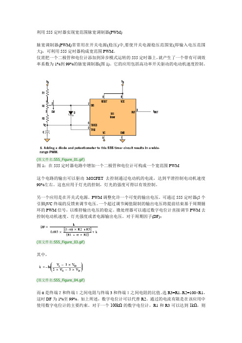
利用555定时器实现宽范围脉宽调制器(PWM)脉宽调制器(PWM)常常用在开关电源(稳压)中,要使开关电源稳压范围宽(即输入电压范围大),可利用555定时器构成宽范围PWM。
仅需把一个二极管和电位计添加到异步模式运转的555定时器上,就产生了一个带有可调效率系数为1%到99%的脉宽调制器(图1)。
它的应用包括高功率开关驱动的电动机速度控制。
(原文件名:555_Figure_01.gif)图1:在555定时器电路中增加一个二极管和电位计可构成一个宽范围PWM这个电路的输出可以驱动MOSFET去控制通过电动机的电流,达到平滑控制电动机速度90%左右。
这也应用于灯光的控制,灯光的强度可得以有效控制。
另一个应用是在开关式电源。
PWM调整允许一个可变的输出电压。
可通过555定时器(5个引脚)VC终端的反馈来调节电压。
一个超过调节阈值限制的输出电压将提前结束基于周期循环的PWM信号,以维持输出电压的稳定。
微处理器可以通过数字电位计直接调节PWM去控制电动机速度、灯光强度或者电源输出电压。
对于周期因子(DF):(原文件名:555_Figure_03.gif)其中,(原文件名:555_Figure_04.gif)而α是终端2和终端1之间电阻与终端3和终端1之间电阻的比值。
选R3=R1,R2=100×R1,这时DF为1%至99%。
如上所述,数字电位计可以代替R2。
通过的电流有限是在该应用中使用数字电位计的主要约束。
对于一个100kΩ的数字电位计,R1和R3可以达到1kΩ,则峰值电流为5mA。
标准二极管可在递减线性下当作D来使用。
对于理想的二极管,k=0.693,则有:(原文件名:555_Figure_05.gif)DF和α之间为线性关系。
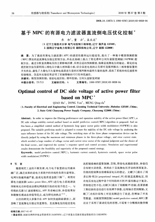
图2显示了当α变化时VOUT的波形。
(原文件名:555_Figure_02.gif)图2:这三个波形显示了VOUT如何随α变化而变化。
作者:Henry Santana,Kavlico Corp=============呵呵,原来在这里8楼就有详细的解释<br><br> (原文件名:图2.gif)=============老外的图,是不是比3.2.3a少接一个VD2?阿莫的楼主位公式是不是应该改成3.2.3b那样?我个人觉得,有了光偶就可以省掉74HC14.有了HC14就可以省去光偶.74HC14换成CD40106如何?这样就不用额外的5V电源了.C2容量较大,是否在7812上并联反向二极管较为保险.印象中的555第3脚,好象拉电流能力强,输出电流好象很弱有一个小细节,有人能解释吗?IRFZ48N 的GS我加入了1K的电阻,是作为GS快速释放电荷使用的。

基于MPC564的发动机电控单元硬件设计/邮件群发发动机电子控制技术是汽车电子领域的关键技术,随着欧洲排放法规的日益严格化,以及对汽车安全、节能、环保、舒适、方便的要求越来越高,发动机电子控制单元的功能也越来越强大,对控制芯片的要求也随之提高。
32位微控制器功能强大,提供了低功耗、高性能的处理能力,目前已经逐渐取代8位、16位微控制器而成为主流应用产品。
我国在汽车发动机电子控制等关键技术领域与国外存在明显的差距,研究具有自主知识产权的发动机电子控制单元对我国的汽车工业发展具有重要的战略意义。
本文基于Freescale公司的32位高性能控制芯片MPC564对赛欧轿车479QE型汽油机进行了电控单元的硬件设计,台架试验表明硬件设计方案可行。
电控单元硬件电路包括输入级电路、微控制器和输出级电路三大部分,其结构框图如图1所示。
1 微控制器根据发动机电控技术的发展趋势,设计中选用了32位高性能微控制器MPC564,其主要功能模块有:·最高主频56M的精简指令集CPU;· 64bit浮点数单元(FPU),支持高级语言编程;· 512KB FLASH+32KB SRAM;·独立工作双时间处理单元(TPU3);·模块化输入输出系统(MIOS);·双队列模数转换模块(QADC);·三个CAN2.0B控制器模块(TOUCAN);·增强型队列串行多通道模块(QSMCM)。
MPC564微控制器不仅具有高速运算、实时输入和输出、高速AD转换的能力,同时其卓越的集成模块,如TPU、CAN等专门为汽车电子量身定制,使得电控单元无需过多外接功能驱动芯片,硬件布线减少,成本降低,有助于提高系统的可靠性。
2 输入级电路(1)电源管理模块系统的硬件设计中,电源部分占有重要地位,它直接影响系统的稳定性、可靠性和抗干扰能力。
PC33994是Freescale公司的一款中等功率的集成芯片,它能提供5V 和2.6V的微控制器主电源以及5V的传感器供电电源,同时还带有3.3V备用电源。

Freescale Semiconductor Data Sheet: Technical DataContentsDocument Number: MPC5554Rev. 3.0, 11/2008This document provides electrical specifications, pin assignments, and package diagrams for the MPC5554 microcontroller device. For functional characteristics, refer to the MPC5553/MPC5554 Microcontroller Reference Manual .1OverviewThe MPC5554 microcontroller (MCU) is a member of the MPC5500 family of microcontrollers built on the Power Architecture™ embedded technology. Thisfamily of parts has many new features coupled with high performance CMOS technology to provide substantial reduction of cost per feature and significant performance improvement over the MPC500 family.The host processor core of this device complies with the Power Architecture embedded category that is 100% user-mode compatible (including floating point library) with the original Power PC™ user instruction set architecture (UISA). The embedded architectureenhancements improve the performance in embedded applications. The core also has additional instructions, including digital signal processing (DSP) instructions, beyond the original Power PC instruction set.1Overview . . . . . . . . . . . . . . . . . . . . . . . . . . . . . . . . . . . . . 12Ordering Information . . . . . . . . . . . . . . . . . . . . . . . . . . . . 33Electrical Characteristics. . . . . . . . . . . . . . . . . . . . . . . . . 43.1Maximum Ratings . . . . . . . . . . . . . . . . . . . . . . . . . . 43.2Thermal Characteristics . . . . . . . . . . . . . . . . . . . . . 53.3Package. . . . . . . . . . . . . . . . . . . . . . . . . . . . . . . . . . 83.4EMI Characteristics. . . . . . . . . . . . . . . . . . . . . . . . . 83.5ESD Characteristics . . . . . . . . . . . . . . . . . . . . . . . . 93.6VRC and POR Electrical Specifications . . . . . . . . . 93.7Power-Up/Down Sequencing. . . . . . . . . . . . . . . . . 103.8DC Electrical Specifications . . . . . . . . . . . . . . . . . 133.9Oscillator and FMPLL Electrical Characteristics . . 203.10eQADC Electrical Characteristics . . . . . . . . . . . . . 223.11H7Fa Flash Memory Electrical Characteristics . . . 233.12AC Specifications . . . . . . . . . . . . . . . . . . . . . . . . . 243.13AC Timing . . . . . . . . . . . . . . . . . . . . . . . . . . . . . . . 264Mechanicals. . . . . . . . . . . . . . . . . . . . . . . . . . . . . . . . . . 454.1MPC5554 416 PBGA Pinout. . . . . . . . . . . . . . . . . 454.2MPC5554 416-Pin Package Dimensions . . . . . . . 485Revision History for the MPC5554 Data Sheet . . . . . . . 505.1Changes to Revision 2 in Revision 3. . . . . . . . . . . 50MPC5554Microcontroller Data Sheetby:Microcontroller DivisionOverviewThe MPC5500 family of parts contains many new features coupled with high performance CMOS technology to provide significant performance improvement over the MPC565.The MPC5554 has two levels of memory hierarchy. The fastest accesses are to the 32-kilobytes (KB) unified cache. The next level in the hierarchy contains the 64-KB on-chip internal SRAM andtwo-megabytes (MB) internal flash memory. The internal SRAM and flash memory hold instructions and data. The external bus interface is designed to support most of the standard memories used with the MPC5xx family.The complex input/output timer functions of the MPC5554 are performed by two enhanced time processor unit (eTPU) engines. Each eTPU engine controls 32 hardware channels, providing a total of 64 hardware channels. The eTPU has been enhanced over the TPU by providing: 24-bit timers, double-action hardware channels, variable number of parameters per channel, angle clock hardware, and additional control and arithmetic instructions. The eTPU is programmed using a high-level programming language.The less complex timer functions of the MPC5554 are performed by the enhanced modular input/output system (eMIOS). The eMIOS’ 24 hardware channels are capable of single-action, double-action,pulse-width modulation (PWM), and modulus-counter operations. Motor control capabilities include edge-aligned and center-aligned PWM.Off-chip communication is performed by a suite of serial protocols including controller area networks (FlexCANs), enhanced deserial/serial peripheral interfaces (DSPIs), and enhanced serial communications interfaces (eSCIs). The DSPIs support pin reduction through hardware serialization and deserialization of timer channels and general-purpose input/output (GPIOs) signals.The MCU has an on-chip enhanced queued dual analog-to-digital converter (eQADC). The 416 package has 40-channels.The system integration unit (SIU) performs several chip-wide configuration functions. Pad configuration and general-purpose input and output (GPIO) are controlled from the SIU. External interrupts and reset control are also determined by the SIU. The internal multiplexer submodule (SIU_DISR) provides multiplexing of eQADC trigger sources, daisy chaining the DSPIs, and external interrupt signal multiplexing.Ordering Information2Ordering InformationFigure 1. MPC5500 Family Part Number ExampleUnless noted in this data sheet, all specifications apply from T L to T H .Table 1. Orderable Part NumbersFreescale Part Number 1All devices are PPC5554, rather than MPC5554, until product qualifications are complete. Not all configurations are available in the PPC parts.Package DescriptionSpeed (MHz)Operating Temperature 22The lowest ambient operating temperature is referenced by T L ; the highest ambient operating temperature is referenced by T H.Nominal Max. 3 (f MAX )3Speed is the nominal maximum frequency. Max. speed is the maximum speed allowed including frequency modulation (FM). 82 MHz parts allow for 80 MHz system clock + 2% FM; 114 MHz parts allow for 112 MHz system clock + 2% FM; and132 MHz parts allow for 128MHz system clock +2% FM.Min. (T L )Max.(T H )MPC5554MVR132MPC5554 416 package Lead-free (PbFree)132132 –40° C 125° C MPC5554MVR112112114MPC5554MVR808082MPC5554AVR132132132–55° C 125° C MPC5554MZP132MPC5554 416 packageLeaded (SnPb)132132 –40° C 125° C MPC5554MZP112112114MPC5554MZP808082MPC5554AZP132132132–55° C125° CM PC M 80R Qualification statusCore codeDevice numberTemperature range Package identifierOperating frequency (MHz)T ape and reel status Temperature Range M = –40° C to 125° C A = –55° C to 125° CPackage Identifier ZP = 416PBGA SnPb VR = 416PBGA Pb-freeOperating Frequency 80 = 80 MHz 112 = 112 MHz 132 = 132 MHzTape and Reel Status R2 = Tape and reel (blank) = T raysQualification Status P = Pre qualification M = Fully spec. qualified5554ZP Note: Not all options are available on all devices. Refer to Table 1.2Electrical Characteristics3Electrical CharacteristicsThis section contains detailed information on power considerations, DC/AC electrical characteristics, and AC timing specifications for the MCU.3.1Maximum RatingsTable2. Absolute Maximum Ratings1Spec Characteristic Symbol Min.Max.Unit1 1.5 V core supply voltage 2V DD–0.3 1.7V2Flash program/erase voltage V PP–0.3 6.5V 4Flash read voltage V FLASH–0.3 4.6V 5SRAM standby voltage V STBY–0.3 1.7V 6Clock synthesizer voltage V DDSYN–0.3 4.6V7 3.3 V I/O buffer voltage V DD33–0.3 4.6V8Voltage regulator control input voltage V RC33–0.3 4.6V 9Analog supply voltage (reference to V SSA)V DDA–0.3 5.5V 10I/O supply voltage (fast I/O pads) 3V DDE–0.3 4.6V 11I/O supply voltage (slow and medium I/O pads) 3V DDEH–0.3 6.5V12DC input voltage 4V DDEH powered I/O padsV DDE powered I/O pads V IN–1.0 5–1.0 56.5 64.6 7V13Analog reference high voltage (reference to V RL)V RH–0.3 5.5V 14V SS to V SSA differential voltage V SS – V SSA–0.10.1V 15V DD to V DDA differential voltage V DD – V DDA–V DDA V DD V 16V REF differential voltage V RH – V RL–0.3 5.5V 17V RH to V DDA differential voltage V RH – V DDA–5.5 5.5V 18V RL to V SSA differential voltage V RL – V SSA–0.30.3V 19V DDEH to V DDA differential voltage V DDEH – V DDA–V DDA V DDEH V 20V DDF to V DD differential voltage V DDF – V DD–0.30.3V 21 V RC33 to V DDSYN differential voltage spec has been moved to Table9 DC Electrical Specifications, Spec 43a.22V SSSYN to V SS differential voltage V SSSYN – V SS–0.10.1V 23V RCVSS to V SS differential voltage V RCVSS – V SS–0.10.1V 24Maximum DC digital input current 8(per pin, applies to all digital pins)4I MAXD–22mA25Maximum DC analog input current 9(per pin, applies to all analog pins)I MAXA–33mA26Maximum operating temperature range 10Die junction temperatureT J T L150.0o C 27Storage temperature range T STG–55.0150.0o CElectrical Characteristics3.2Thermal CharacteristicsThe shaded rows in the following table indicate information specific to a four-layer board.28Maximum solder temperature 11Lead free (Pb-free)Leaded (SnPb)T SDR ——260.0245.0oC29Moisture sensitivity level 12MSL—3Functional operating conditions are given in the DC electrical specifications. Absolute maximum ratings are stress ratings only, and functional operation at the maxima is not guaranteed. Stress beyond any of the listed maxima can affect device reliability or cause permanent damage to the device.21.5 V ± 10% for proper operation. This parameter is specified at a maximum junction temperature of 150 o C.3All functional non-supply I/O pins are clamped to V SS and V DDE , or V DDEH .4AC signal overshoot and undershoot of up to ± 2.0 V of the input voltages is permitted for an accumulative duration of 60 hours over the complete lifetime of the device (injection current not limited for this duration).5Internal structures hold the voltage greater than –1.0 V if the injection current limit of 2 mA is met. Keep the negative DC voltage greater than –0.6 V on eTPUB[15] and SINB during the internal power-on reset (POR) state.6Internal structures hold the input voltage less than the maximum voltage on all pads powered by VDDEH supplies, if themaximum injection current specification is met (2 mA for all pins) and V DDEH is within the operating voltage specifications.7Internal structures hold the input voltage less than the maximum voltage on all pads powered by V DDE supplies, if the maximum injection current specification is met (2 mA for all pins) and V DDE is within the operating voltage specifications.8T otal injection current for all pins (including both digital and analog) must not exceed 25 mA.9T otal injection current for all analog input pins must not exceed 15 mA.10Lifetime operation at these specification limits is not guaranteed.11Moisture sensitivity profile per IPC/JEDEC J-STD-020D.12Moisture sensitivity per JEDEC test method A112.Table 3. MPC5554 Thermal CharacteristicsSpec MPC5554 Thermal CharacteristicSymbol 416 PBGAUnit 1Junction to ambient 1, 2, natural convection (one-layer board)Junction temperature is a function of on-chip power dissipation, package thermal resistance, mounting site (board) temperature, ambient temperature, air flow, power dissipation of other components on the board, and board thermal resistance.2Per SEMI G38-87 and JEDEC JESD51-2 with the single-layer board horizontal.R θJA 24°C/W 2Junction to ambient 1, 3, natural convection (four-layer board 2s2p)3Per JEDEC JESD51-6 with the board horizontal.R θJA 18°C/W 3Junction to ambient 1, 3 (@200 ft./min., one-layer board)R θJMA 19°C/W 4Junction to ambient 1, 3 (@200 ft./min., four-layer board 2s2p)R θJMA 15°C/W 5Junction to board 4 (four-layer board 2s2p)4Thermal resistance between the die and the printed circuit board per JEDEC JESD51-8. Board temperature is measured on the top surface of the board near the package.R θJB 9°C/W 6Junction to case 55Indicates the average thermal resistance between the die and the case top surface as measured by the cold plate method (MIL SPEC-883 Method 1012.1) with the cold plate temperature used for the case temperature.R θJC 5°C/W 7Junction to package top 6, natural convection6Thermal characterization parameter indicating the temperature difference between package top and the junction temperature per JEDEC JESD51-2.ΨJT2°C/WTable 2. Absolute Maximum Ratings 1 (continued)Spec CharacteristicSymbol Min.Max.UnitElectrical Characteristics3.2.1General Notes for Specifications at Maximum Junction Temperature, can be obtained from the equation:An estimation of the device junction temperature, TJT J = T A + (RθJA× P D)where:T A = ambient temperature for the package (o C)RθJA = junction to ambient thermal resistance (o C/W)P D = power dissipation in the package (W)The thermal resistance values used are based on the JEDEC JESD51 series of standards to provide consistent values for estimations and comparisons. The difference between the values determined for the single-layer (1s) board compared to a four-layer board that has two signal layers, a power and a ground plane (2s2p), demonstrate that the effective thermal resistance is not a constant. The thermal resistance depends on the:•Construction of the application board (number of planes)•Effective size of the board which cools the component•Quality of the thermal and electrical connections to the planes•Power dissipated by adjacent componentsConnect all the ground and power balls to the respective planes with one via per ball. Using fewer vias to connect the package to the planes reduces the thermal performance. Thinner planes also reduce the thermal performance. When the clearance between the vias leave the planes virtually disconnected, the thermal performance is also greatly reduced.As a general rule, the value obtained on a single-layer board is within the normal range for the tightly packed printed circuit board. The value obtained on a board with the internal planes is usually within the normal range if the application board has:•One oz. (35 micron nominal thickness) internal planes•Components are well separated•Overall power dissipation on the board is less than 0.02 W/cm2The thermal performance of any component depends on the power dissipation of the surrounding components. In addition, the ambient temperature varies widely within the application. For many natural convection and especially closed box applications, the board temperature at the perimeter (edge) of the package is approximately the same as the local air temperature near the device. Specifying the local ambient conditions explicitly as the board temperature provides a more precise description of the local ambient conditions that determine the temperature of the device.Electrical CharacteristicsAt a known board temperature, the junction temperature is estimated using the following equation:T J = T B + (R θJB × P D )where:T J = junction temperature (o C)T B = board temperature at the package perimeter (o C/W)R θJB = junction-to-board thermal resistance (o C/W) per JESD51-8P D = power dissipation in the package (W)When the heat loss from the package case to the air does not factor into the calculation, an acceptable value for the junction temperature is predictable. Ensure the application board is similar to the thermal test condition, with the component soldered to a board with internal planes.The thermal resistance is expressed as the sum of a junction-to-case thermal resistance plus a case-to-ambient thermal resistance:R θJA = R θJC + R θCA where:R θJA = junction-to-ambient thermal resistance (o C/W)R θJC = junction-to-case thermal resistance (o C/W)R θCA = case-to-ambient thermal resistance (o C/W)R θJC is device related and is not affected by other factors. The thermal environment can be controlled to change the case-to-ambient thermal resistance, R θCA . For example, change the air flow around the device, add a heat sink, change the mounting arrangement on the printed circuit board, or change the thermal dissipation on the printed circuit board surrounding the device. This description is most useful for packages with heat sinks where 90% of the heat flow is through the case to heat sink to ambient. For most packages, a better model is required.A more accurate two-resistor thermal model can be constructed from the junction-to-board thermal resistance and the junction-to-case thermal resistance. The junction-to-case thermal resistance describes when using a heat sink or where a substantial amount of heat is dissipated from the top of the package. The junction-to-board thermal resistance describes the thermal performance when most of the heat is conducted to the printed circuit board. This model can be used to generate simple estimations and for computational fluid dynamics (CFD) thermal models.To determine the junction temperature of the device in the application on a prototype board, use the thermal characterization parameter (ΨJT ) to determine the junction temperature by measuring the temperature at the top center of the package case using the following equation:T J = T T + (ΨJT × P D )where:T T = thermocouple temperature on top of the package (o C)ΨJT = thermal characterization parameter (o C/W)P D = power dissipation in the package (W)Electrical CharacteristicsThe thermal characterization parameter is measured in compliance with the JESD51-2 specification using a 40-gauge type T thermocouple epoxied to the top center of the package case. Position the thermocouple so that the thermocouple junction rests on the package. Place a small amount of epoxy on the thermocouple junction and approximately 1 mm of wire extending from the junction. Place the thermocouple wire flat against the package case to avoid measurement errors caused by the cooling effects of the thermocouple wire.References:Semiconductor Equipment and Materials International 3081 Zanker Rd.San Jose, CA., 95134(408) 943-6900MIL-SPEC and EIA/JESD (JEDEC) specifications are available from Global Engineering Documents at 800-854-7179 or 303-397-7956.JEDEC specifications are available on the web at .1. C.E. Triplett and B. Joiner, “An Experimental Characterization of a 272 PBGA Within an Automotive Engine Controller Module,” Proceedings of SemiTherm, San Diego, 1998, pp. 47–54.2.G . Kromann, S. Shidore, and S. Addison, “Thermal Modeling of a PBGA for Air-Cooled Applica-tions,” Electronic Packaging and Production, pp. 53–58, March 1998.3. B. Joiner and V . Adams, “Measurement and Simulation of Junction to Board Thermal Resistance and Its Application in Thermal Modeling,” Proceedings of SemiTherm, San Diego, 1999, pp. 212–220.3.3PackageThe MPC5554 is available in packaged form. Read the package options in Section 2, “Ordering Information.” Refer to Section 4, “Mechanicals,” for pinouts and package drawings.3.4EMI (Electromagnetic Interference) CharacteristicsTable 4. EMI Testing Specifications 1EMI testing and I/O port waveforms per SAE J1752/3 issued 1995-03. Qualification testing was performed on the MPC5554 and applied to the MPC5500 family as generic EMI performance data. Spec CharacteristicMinimum Typical Maximum Unit 1Scan range 0.15—1000MHz 2Operating frequency ——f MAX MHz 3V DD operating voltages— 1.5—V 4V DDSYN , V RC33, V DD33, V FLASH , V DDE operating voltages — 3.3—V 5V PP , V DDEH , V DDA operating voltages — 5.0—V 6Maximum amplitude ——14 232 32Measured with the single-chip EMI program.3Measured with the expanded EMI program.dBuV7Operating temperature——25oCElectrical Characteristics3.5ESD (Electromagnetic Static Discharge) Characteristics3.6Voltage Regulator Controller (V RC ) andPower-On Reset (POR) Electrical SpecificationsThe following table lists the V RC and POR electrical specifications:Table 5. ESD Ratings 1, 21All ESD testing conforms to CDF-AEC-Q100 Stress T est Qualification for Automotive Grade Integrated Circuits.2Device failure is defined as: ‘If after exposure to ESD pulses, the device does not meet the device specification requirements, which includes the complete DC parametric and functional testing at room temperature and hot temperature.Characteristic SymbolValue Unit ESD for human body model (HBM)2000V HBM circuit descriptionR11500ΩC100pFESD for field induced charge model (FDCM)500 (all pins)V 750 (corner pins)Number of pulses per pin:Positive pulses (HBM)Negative pulses (HBM)——11——Interval of pulses—1second Table 6. V RC and POR Electrical SpecificationsSpec CharacteristicSymbol Min.Max.Units 11.5 V(V DD ) POR 1Negated (ramp up)Asserted (ramp down)V POR151.11.1 1.351.35V23.3 V(V DDSYN ) POR 1Asserted (ramp up)Negated (ramp up)Asserted (ramp down)Negated (ramp down)V POR330.02.02.00.00.302.852.850.30V3RESET pin supply (V DDEH6) POR 1, 2Negated (ramp up)Asserted (ramp down) V POR5 2.02.0 2.852.85V 4V RC33 voltageBefore V RC allows the pass transistor to start turning onV TRANS_START 1.0 2.0V 5When V RC allows the passtransistor to completely turn on 3, 4V TRANS_ON 2.02.85V6When the voltage is greater than the voltage at which the V RC keeps the 1.5 V supply in regulation 5, 6V VRC33REG3.0—V – 55o C 711.0—mA Current can be sourced – 40oC 11.0—mA 7by V RCCTL at Tj:25o C I VRCCTL 89.0—mA 150o C7.5—mAElectrical Characteristics3.7Power-Up/Down SequencingPower sequencing between the 1.5 V power supply and V DDSYN or the RESET power supplies is required if using an external 1.5 V power supply with V RC33 tied to ground (GND). To avoid power-sequencing, V RC33 must be powered up within the specified operating range, even if the on-chip voltage regulator controller is not used. Refer to Section 3.7.2, “Power-Up Sequence (VRC33 Grounded),” and Section 3.7.3, “Power-Down Sequence (VRC33 Grounded).”Power sequencing requires that V DD33 must reach a certain voltage where the values are read as ones before the POR signal negates. Refer to Section 3.7.1, “Input Value of Pins During POR Dependent on VDD33.”Although power sequencing is not required between V RC33 and V DDSYN during power up, V RC33 must not lead V DDSYN by more than 600 mV or lag by more than 100 mV for the V RC stage turn-on to operate within specification. Higher spikes in the emitter current of the pass transistor occur if V RC33 leads or lags V DDSYN by more than these amounts. The value of that higher spike in current depends on the board power supply circuitry and the amount of board level capacitance.8Voltage differential during power up such that:V DD33 can lag V DDSYN or V DDEH6 before V DDSYN and V DDEH6 reach the V POR33 and V POR5 minimums respectively.V DD33_LAG— 1.0V 9Absolute value of slew rate on power supply pins ——50V/ms 10Required gain at Tj:I DD ÷ I VRCCTL (@ f sys = f MAX )6, 8, 9, 10– 55o C 7BET A 1170——– 40o C70——25o C8511——150o C10511500—1The internal POR signals are V POR15, V POR33, and V POR5RESET must remain asserted until the power supplies are within the operating conditions as specified in T able 9 DC Electrical internal POR asserts.2V IL_S (T able 9, Spec15) is guaranteed to scale with V DDEH6 down to V POR5.3Supply full operating current for the 1.5 V supply when the 3.3 V supply reaches this range.4It is possible to reach the current limit during ramp up—do not treat this event as short circuit current.5At peak current for device.6Requires compliance with Freescale’s recommended board requirements and transistor recommendations. Board signal traces/routing from the V RCCTL package signal to the base of the external pass transistor and between the emitter of the pass transistor to the V DD package signals must have a maximum of 100 nH inductance and minimal resistance(less than 1 Ω). V RCCTL must have a nominal 1 μF phase compensation capacitor to ground. V DD must have a 20 μF (nominal) bulk capacitor (greater than 4 μF over all conditions, including lifetime). Place high-frequency bypass capacitors consisting of eight 0.01 μF , two 0.1 μF , and one 1 μF capacitors around the package on the V DD supply signals.7Only available on devices that support -55o C.8I VRCCTL is measured at the following conditions: V DD = 1.35 V , V RC33 = 3.1 V , V VRCCTL = 2.2 V .9Refer to T able 1 for the maximum operating frequency.10Values are based on I DD from high-use applications as explained in the I DD Electrical Specification. 11BET A represents the worst-case external transistor. It is measured on a per-part basis and calculated as (I DD ÷ I VRCCTL ).Table 6. V RC and POR Electrical Specifications (continued)Spec CharacteristicSymbol Min.Max.UnitsFurthermore, when all of the PORs negate, the system clock starts to toggle, adding another large increase of the current consumed by V RC33. If V RC33 lags V DDSYN by more than 100 mV , the increase in current consumed can drop V DD low enough to assert the 1.5 V POR again. Oscillations are possible when the 1.5V POR asserts and stops the system clock, causing the voltage on V DD to rise until the 1.5V POR negates again. All oscillations stop when V RC33 is powered sufficiently.When powering down, V RC33 and V DDSYN have no delta requirement to each other, because the bypass capacitors internal and external to the device are already charged. When not powering up or down, no delta between V RC33 and V DDSYN is required for the V RC to operate within specification.There are no power up/down sequencing requirements to prevent issues such as latch-up, excessive current spikes, and so on. Therefore, the state of the I/O pins during power up and power down varies depending on which supplies are powered.Table 7 gives the pin state for the sequence cases for all pins with pad type pad_fc (fast type).Table 8 gives the pin state for the sequence cases for all pins with pad type pad_mh (medium type) and pad_sh (slow type).The values in Table 7 and Table 8 do not include the effect of the weak-pull devices on the output pins during power up.Before exiting the internal POR state, the pins go to a high-impedance state until POR negates. When the internal POR negates, the functional state of the signal during reset applies and the weak-pull devices (up or down) are enabled as defined in the device reference manual. If V DD is too low to correctly propagate the logic signals, the weak-pull devices can pull the signals to V DDE and V DDEH .To avoid this condition, minimize the ramp time of the V DD supply to a time period less than the time required to enable the external circuitry connected to the device outputs.Table 7. Pin Status for Fast Pads During the Power SequenceV DDE V DD33V DD POR Pin Status for Fast Pad Output Driverpad_fc (fast)Low ——Asserted Low V DDE Low Low Asserted High V DDE Low V DD Asserted HighV DDE V DD33Low Asserted High impedance (Hi-Z)V DDE V DD33V DD Asserted Hi-Z V DDEV DD33V DDNegatedFunctionalTable 8. Pin Status for Medium and Slow Pads During the Power SequenceV DDEH V DD POR Pin Status for Medium and Slow Pad Output Driverpad_mh (medium) pad_sh (slow)Low —Asserted LowV DDEH Low Asserted High impedance (Hi-Z)V DDEH V DD Asserted Hi-Z V DDEHV DDNegatedFunctional3.7.1Input Value of Pins During POR Dependent on V DD33When powering up the device, V DD33 must not lag the latest V DDSYN or RESET power pin (V DDEH6) by more than the V DD33 lag specification listed in Table6, spec 8. This avoids accidentally selecting the bypass clock mode because the internal versions of PLLCFG[0:1] and RSTCFG are not powered and therefore cannot read the default state when POR negates. V DD33 can lag V DDSYN or the RESET power pin (V DDEH6), but cannot lag both by more than the V DD33 lag specification. This V DD33 lag specification applies during power up only. V DD33 has no lead or lag requirements when powering down.3.7.2Power-Up Sequence (V RC33 Grounded)The 1.5V V DD power supply must rise to 1.35V before the 3.3V V DDSYN power supply and the RESET power supply rises above 2.0 V. This ensures that digital logic in the PLL for the 1.5V power supply does not begin to operate below the specified operation range lower limit of 1.35V. Because the internal 1.5V POR is disabled, the internal 3.3V POR or the RESET power POR must hold the device in reset. Since they can negate as low as 2.0V, V DD must be within specification before the 3.3V POR and the RESET POR negate.V DDSYNV DD2.0 V1.35 VV DD must reach 1.35 V before V DDSYN and the RESET power reach 2.0 VFigure2. Power-Up Sequence (V RC33 Grounded)3.7.3Power-Down Sequence (V RC33 Grounded)The only requirement for the power-down sequence with V RC33 grounded is if V DD decreases to less than its operating range, V DDSYN or the RESET power must decrease to less than 2.0V before the V DD power increases to its operating range. This ensures that the digital 1.5V logic, which is reset only by an ORed POR and can cause the 1.5V supply to decrease less than its specification value, resets correctly. See Table6, footnote 1.。

自动变速器TCU解决方案摘要:基于RapidECU的自动变速器TCU快速开发解决方案,可以支持液动、气动和电机三种不同执行机构的自动变速器,使用户可以在数周内完成TCU原型样机的开发,实现离合器控制,选换挡操作和发动机接管控制等基本功能,在数月内完成批量产品样件的开发,实现中小批量装车试验,为自动变速器TCU大批量产业化打下良好基础。
概述自动变速器能够实现车辆自动起步,自动换挡,提高驾驶舒适性,减少驾驶员疲劳。
自动变速器还能够提高整车动力性,改善燃油经济性和排放,已经逐渐成为现代汽车的基本配置。
目前市场上常见的自动变速器有机械式自动变速器(AMT)、机械式无级自动变速器(CVT)、液力机械式自动变速器(AT)和双离合器式自动变速器(DCT)四种类型,按照执行机构不同可分为液动、气动和电机三种类型。
自动变速器系统是由TCU、选换挡机构及离合器机构组成,其中TCU采集传感器信息及CAN总线数据,经过运算处理后,控制执行机构动作,实现选换挡、离合器动作及发动机接管控制等,是自动变速器控制系统的核心。
TCU电控单元主要包括控制器硬件和控制器软件,其中的控制器软件又包括基础软件与应用软件。
由于TCU电控系统执行机构的多样性及复杂性,无论是控制器硬件开发,还是基础软件或者应用软件开发都需要花费大量的时间、精力以及昂贵的费用。
如果没有合适的开发工具,TCU的研发和产业化几乎成了难以完成的任务。
使用RapidECU快速原型控制器可以在没有控制器硬件的情况下,提前进行控制算法的开发与验证,尤其适合于自动变速器等复杂系统电控单元的开发研究,快速原型的试验结果还可以为产品硬件设计提供参考。
因此,控制器快速原型在进行软件快速验证的同时,也降低了硬件返工几率,从而缩短开发周期,降低开发成本,提高控制器设计质量。
开发流程开发流程符合国际标准的V型开发模式,基于MATLAB\Simulink\Stateflow\ECUCoder图形化建模方式建立软件工程,完全零手工的一键式全自动代码生成,可以同时完成应用软件和基础软件模型自动代码生成,在开发过程中随时保持模型和代码的同步状态。
JTAG模式下的MPC5554外部FLASH编程的设计与实现/摘要:在分析Freescale公司32位微控制器MPC5554的FLASH编程特性基础上,完成了MPC5554外部扩展FLASH存储器的软、硬件设计。
研究利用Codewarrior编译器、P&E调试器与JTAG接口模式组合的软件开发平台实现外部FLASH编程的软件属性配置及编程设计。
重点研究MPC5554相关寄存器配置实现与JTAG模式下对AM29LV160DT进行擦除和写入的编程原理。
该设计成功实现JTAG模式下对MPC5554外部FLASH存储器编程,为利用MPC5554实现复杂多变量控制系统打下基础。
关键词:MPC5554;AM29LV160DT;JTAG;FLASH编程中图分类号:TP3110引言随着信息技术的发展,嵌入式系统越来越广泛地应用于手机通信、汽车、航空航天、工业控制等领域。
在这些电子产品中,大多以嵌入式微处理器为核心,配套相关的外围辅助设备,对控制对象进行软硬件的功能剪裁性设计,并将控制程序固化在非易失性存储器中。
FLASH作为一种存储速度快,容量大,可多次擦写并且价格便宜的存储器得到了广泛的应用。
由于有些微处理器内部不包含FLASH或FLASH存储空间太小、擦写次数有限,为了提供足够的程序存储空间,需要对其进行外部FLASH扩展。
JTAG是目前广泛使用的一种系统在线编程的模式,大大方便了嵌入式系统下载程序至FLASH。
该设计使用的微处理器为MPC5554,通过JTAG接口对外扩FLASH进行编程。
1MPC5554简介[JP2]MPC5554是Freescale公司推出的采用PowerPC内核的一款32位微控制器,属于MPC5500系列第一代产品,可用于航空航天、汽车、工业控制等嵌入式系统中。
如图1所示,MPC5554内部带有浮点运算单元,集成DSP运算指令,拥有较高的计算能力,可以满足多任务处理和实时控制的要求。
基于MPC5554的飞机二次配电设备多路采样的设计
赵桂铭;张晓斌;郑先成
【期刊名称】《机电一体化》
【年(卷),期】2011()8
【摘要】分析了以32位PowerPC微控制器MPC5554为核心的飞机二次配电设备的结构和功能,介绍了MPC5554中eQADC(增强型序列模数转换)模块的工作机制。
针对MPC5554进行多路模拟信号采样数据存取量大的问题,提出了一种由eDMA辅助完成多路采样的方法,并以嵌入式操作系统μC/OS-Ⅱ为平台对多路采样实时任务进行了设计。
飞机地面电网试验表明,该系统运行稳定可靠,能够实时准确采集多路信号,并显著提高了主CPU的效率。
【总页数】5页(P75-78)
【关键词】MPC5554;多路采样;DMA;μC/OS-11;SPDA
【作者】赵桂铭;张晓斌;郑先成
【作者单位】西北工业大学自动化学院
【正文语种】中文
【中图分类】TP274.2
【相关文献】
1.基于MPC5634的汽车控制器多路AD采样的设计 [J], 蔡余喜;赵震
2.基于AD7266的多路2Ms/s同步采样A/D模块的设计 [J], 贾晓华;唐辉
3.基于LabVIEW的飞机二次配电管理装置(SPDA)测试系统设计 [J], 张晓斌;石海
平;陈艳;雷涛
4.基于双DSP的航空二次配电设备控制系统的设计与实现 [J], 吴小华;马亮;董延军;高红
5.基于CPLD和DSP的不同采样速率多路数据采集系统的设计 [J], 周杰;陈贤祥;杨集;任仁;夏善红
因版权原因,仅展示原文概要,查看原文内容请购买。
基于MPC5534的共轨系统eTPU代码开发
高先进;杭勇;龚笑舞;施华传;王伏
【期刊名称】《现代车用动力》
【年(卷),期】2011(000)002
【摘要】为满足共轨系统对控制精度和可靠性的严格要求,以MPC5534单片机为平台,开发了eTPU齿捕获函数和执行器控制函数,实验表明,齿捕获函数具有强抗干扰能力和智能判缸逻辑,执行器控制函数以角度为单位,不需要中断参与,控制精度和效率更高,系统满足实际要求.
【总页数】4页(P13-16)
【作者】高先进;杭勇;龚笑舞;施华传;王伏
【作者单位】中国一汽无锡油泵油嘴研究所,江苏,无锡,214063;中国一汽无锡油泵油嘴研究所,江苏,无锡,214063;中国一汽无锡油泵油嘴研究所,江苏,无锡,214063;中国一汽无锡油泵油嘴研究所,江苏,无锡,214063;中国一汽无锡油泵油嘴研究所,江苏,无锡,214063
【正文语种】中文
【中图分类】TK423.8
【相关文献】
1.基于数据库的共轨系统正向设计开发 [J], 黄见;庄凤芝;臧娈
2.一种基于MPC5534的共轨系统新的底层驱动开发 [J], 黄城健;曾伟;宋国民;谢宏斌;高先进
3.基于转矩的柴油机高压共轨系统控制算法开发 [J], 杭勇;龚笑舞;王伏;胡川
4.基于Django快速开发社会化程序代码共享系统(二)——程序代码相关操作的实现 [J], 刘班
5.基于代码自动生成技术的小程序辅助开发系统设计与实现 [J], 彭淑燕;刘思聪因版权原因,仅展示原文概要,查看原文内容请购买。
基于555时基芯片的直流电机PWM控制系统设计【摘要】针对目前笔记本电脑便携式散热器风扇是固定转速,在满足笔记本散热的前提下,存在电能浪费的现象,本文针对笔记本电脑散热需要,设计了一种基于555时基芯片的直流电机风扇PWM控制系统,实现根据实际需要,自动调节风扇的转速,实现了高效、节能。
【关键词】555;PWM笔记本电脑因为其轻便易携而广受大家的喜爱,但随着社会的发展及其应用的日益广泛,使用者对笔记本电脑性能的要求也越来越高,很多笔记本电脑应用了高频率双核处理器、大容量高转速硬盘、高显存显卡、大容量内存等,而同时笔记本电脑的体积正在日益减小。
笔记本电脑工作时的温度的上升,使得笔记本的工作效率下降,并且可能影响到笔记本的使用寿命,因此散热问题无疑是使用者需要考虑的一个大问题。
目前市场上出现了针对笔记本的散热器,但是这些散热器都是恒功率的工作,即使CPU温度在正常范围内,它也照常运转,而它们很多时候都是USB供电的,这样就比较浪费电能,大大的减小了笔记本的使用时间。
本文提出了一种基于555时基芯片的PWM电脑风扇控制系统设计,使得电脑风扇能够根据笔记本的温度进行自动调节转速,实现既能降温又能节能,延长笔记本的使用时间。
PWM控制输出电压波形如图1所示,图中输入直流电压为Ud,输出为加在电机的电枢两端的电压u0,开关管的导通时间为ton,关断时间为toff,开关周期为T。
图1 PWM控制输出电压波形定义占空比为,根据输出电压平均值为可知,通过改变占空比,就可以实现输出电压平均值的调节。
如果通过改变开关管的导通时间为ton,同时保持开关周期T不变来实现输出电压控制的方式就是PWM控制技术。
555定时器是一种模拟和数字功能相结合的集成器件。
它工作电源电压范围宽,可工作于4.5V~16V。
输出最大驱动电流可达200mA。
555定时器成本低,性能可靠,外围电路简单,可以应用于精密定时脉冲宽度调整、脉冲发生器、脉冲位置调整、定时序列、脉冲丢失检测、延时发生器等多种电路。