Additin_RC_2317
- 格式:pdf
- 大小:94.42 KB
- 文档页数:2

I-7018BL 8-channel AI, thermocouple DAQ Module - QuickStart (Dec/2017)I-7018BL8 Channel Voltage Input, Current Input, & Thermocouple Input Data Acquisition ModuleQuick Start GuideProduct Website:https:///i_7018bl.html/dcon_utility_pro.html1. IntroductionI-7018BL is a cost-effective solution for a wide range of valuable industrial control signals and systems. The DCON utility can help users to configure and test I-7018 modules. Plenty of library functions and demo programs are provided to let users develop programs easily under Windows, Linux and DOS operating systems. Users may mount the modules on a DIN rail, panel or wall. Modules have a screw-terminal block to connect to the signals. I-7018 comes with FREE EZ Data Logger Software.2. Terminal Assignment, Block Diagram3. Wiring Diagram4. Default SettingsDefault settings for the I-7018 modules are:▫ Module address: 01▫ Analog input type:Type 08, -10V to 10V, for the I-7017 and I-7019 seriesType 1B, -150V to +150V for the I-7017R-A5Type 0D, -20mA to +20mA for the I-7017C, I-7017FC and I-7017RC Type 05, -2.5V to 2.5V, for the I-7018 series▫ Baud Rate: 9600 bps▫ Checksum disabled▫ Engineering unit format▫ Filter set at 60Hz rejection▫ JP1 set to single-ended mode for I-7018, I-7018P and I-7018BL.I-7018BL 8-channel AI, thermocouple DAQ Module - QuickStart (Dec/2017)5. ConfigurationTo install the module, follow the steps below:1. Connect the analog input.2. Connect the module to the RS-485 network using the DATA+ and DATA- terminals. If the host is only equipped with an RS-232 interface, then an RS-232 to RS-485 converter will be required.3. Connect the module to the power supply using the +Vs and GND terminals. Note that the voltage supplied should be in the range of +10 to +30V DC.I-7018BL 8-channel AI, thermocouple DAQ Module - QuickStart (Dec/2017)4. Open DCON utility proclick on COM port(first icon).It can select multi-options such as Baud Rate, Protocol, Checksum, and Format to search module. The default settings for the module can be found in Section 3. Click OK after selecting the COM port setting.I-7018BL 8-channel AI, thermocouple DAQ Module - QuickStart (Dec/2017)5. DCON utility pro will search for the selected COM port according the setting previously set. DCON Utility Pro supports DCON and Modbus protocol for all ICPDAS and the others modules.6. Configuration I/O module setting on PCI-7018BL 8-channel AI, thermocouple DAQ Module - QuickStart (Dec/2017)7. For I-7000 modules, DCON utility pro terminal can send command to the module. See user manual Sections 2 for details command.Configure the module: sending the %AANNTTCCFF command. See user manual Section 2 for detail commands. To configure the I-7017Z, I-7018Z and I-7019 series, the $AA7CiRrr command must also be sent.Read data from the input channels: send either the #AA or #AAN command to the module.I-7018BL 8-channel AI, thermocouple DAQ Module - QuickStart (Dec/2017)8. If user doesn’t know the command, user can select Address and ID, it will show some refer commands as below. User can select necessary command to test or debug modules.I-7018BL 8-channel AI, thermocouple DAQ Module - QuickStart (Dec/2017)。

//松翰2711程序2018年3月17日,2-7-6-4-8-4-2-9-2 校验码:#include<sn8p2711a.h>#define adc_Start 0X40#define adc_Enable 0x80#define adc_ch_Enable 0x10#define adc_cone 64#define sleep() __asm{SleepMode}unsigned int num,time,codetemp;unsigned int a,b,c,d,e,zc,k,zd0,zd1,zd2;unsigned long zd3;void delayms(unsigned long xms);/***********************************************************ADM 寄存器--------------------------------------------------|ADENB | ADS | EOC | GCHS | - |CHS2 |CHS1 |CHS0 ||------|-----|-----|------|----|-----|-----|-----|************************************************************/ void delayms(unsigned long xms){unsigned long i,j;for(i=xms;i>0;i--)for(j=100;j>0;j--);}void init(void){P0M |= 0x04; //P02 OutputP4M = 0x03; //P40 p41 OutputP5M |= 0x08; //P53 OutputP0UR = 0x04; //P02 P03 pull highP4UR = 0x03; //P41 p41 pull highP5UR = 0x08; //P53 pull highTC1M = 0xd1; //开启计时器,8时钟分频,256阶TC1C = 0xff; //计数255TC1R = 0x80; //调节PWM输出级数最小// TC0M = 0x81; //pwm时间周期设定// TC0C = 0xff;TC0R = 0x80; //控制pwm 占空比TC0M=0x20;TC0C=100;INTRQ=0x00;INTEN=0x20; //打开定时器0和外部中断0中断FGIE = 1;FTC0ENB = 1; //启动定时器d=4;FP40=1;FP02=1;FP41=1;}void main(void){init();while(1){a=0;b=1;while(b){a++;if(a>19){a=0;b--;}}FP02=!FP02;if(FP54==0){a=0;b=0;while(FP54==0){a++;if(a>19)//100us{a=0;b++;}}if((b>60)&&(b<130)){FP40=!FP40;for(a=0;a<5;a++);while(FP54==1);for(a=0;a<5;a++);for(zc=0;zc<4;zc++){for(k=0;k<8;k++){while(FP54==0);a=0;b=8;while(b){a++;if(a>19){a=0;b--;}}if (FP54==1){while(FP54==1);codetemp=codetemp|0x01;if(k<7) codetemp=codetemp<<1;}else if (FP54==0){if(k<7) codetemp=codetemp<<1;}}if(zc==0) zd0=codetemp;if(zc==1) zd1=codetemp;if(zc==2) zd2=codetemp;// if(zc==3) zd3=codetemp;codetemp=0;}a=0;b=230;/*解码成功,下面处理码值*/// if((zd1==0Xff)&&(zd2==0Xff)) R61=!R61;// if(zd2==0X40) R61=!R61;// if((zd0==0x00)&&(zd1==0xff)&&(zd2==0xd8)) R61=!R61; //if((zd0==0X80)&&(zd2==0X20)) R61=!R61;if(zd2==0x40){FP41=!FP41;}else if(zd2==0xa0){}else if(zd2==0xd8){}else if(zd2==0xe0){}else if(zd2==0x10){}else if(zd2==0x90){}while(b){if (FP54==0) b=200;a++;if(a>100){a=0;b--;}}}}}}void __interrupt [0x08] isr(void){if(FTC0IRQ==1){FTC0IRQ=0;TC0C=10;num++;if(num>252) num=0;}}。
![[RCUstall]RCUstall分析,RCUstall内核文档翻译](https://img.taocdn.com/s1/m/5fb4650fc4da50e2524de518964bcf84b9d52da2.png)
[RCUstall]RCUstall分析,RCUstall内核⽂档翻译使⽤RCU的CPU失速检测器本⽂档⾸先讨论RCU的CPU停顿检测器可以定位哪些问题,然后讨论可⽤于微调检测器操作的内核参数和Kconfig选项。
最后,本⽂解释了失速检测器的“splat”格式。
是什么导致RCU CPU停顿警告?是因为您的内核会打印RCU CPU停⽌警告。
下⼀个问题是“是什么原因引起的?” 以下问题可能导致RCU CPU停顿:警告:o RCU read-side 关键部分中出现CPU循环。
o 禁⽤中断时出现CPU循环。
o 禁⽤抢占时出现CPU循环。
这种情况可能会导致RCU调度的停顿,并且,如果使⽤kso??ftirqd,则会导致RCU-bh停顿。
o 下半部禁⽤时出现CPU循环。
这种情况可能导致RCU调度和RCU-bh停顿。
o 对于!CONFIG_PREEMPT内核,CPU可以在内核中的任何位置循环,⽽⽆需调⽤schedule()。
如果确实确实希望在内核中循环,这是您期望的⾏为,则可能需要向cond_resched()添加⼀些调⽤。
o 使⽤太慢的控制台连接来引导Linux,以致⽆法跟上引导时控制台消息的速率。
例如,115Kbaud串⾏控制台的速度可能太慢⽽⽆法跟上启动时消息的速率,经常会导致RCU CPU停顿警告消息。
特别是如果您添加了printk()调试代码。
o 阻⽌RCU宽限期kthread运⾏的任何措施。
这可能会导致“All QSes seen”控制台⽇志消息。
此消息将包含有关kthread上次运⾏的时间以及应该运⾏的频率的信息。
它还可能导致控制台⽇志消息“ rcu _.*kthread starved for”,其中将包含其他调试信息。
O CONFIG_PREEMPT内核中的CPU绑定的实时任务,这可能恰好抢占了RCU读取侧关键部分中间的低优先级任务。
如果不允许该低优先级任务在任何其他CPU上运⾏,则这尤其有害,在这种情况下,下⼀个RCU宽限期将永远⽆法完成,最终将导致系统内存不⾜并挂起。

HF Cobalt CNT 使用手册电源需求:电源:电源供应: 10~30VDC功率 9.6W(400mA@24V)安装环境:操作温度-20℃~50℃存储温度-40℃~85℃湿度: 100%保护等级: IP66抗冲击等级:经过IEC68-2-27测试,EA 30克,11ms,每相3次冲击抗震等级:经过IEC68-2-6测试,FC 1.5mm,10-55Hz,每相2小时安装要点:1.本品为电磁发送接收设备,大面积金属对其正常工作影响比较大,因此必须保证天线的15厘米范围内无大面积金属物品2.本产品连接电缆应远离裸露电缆和高压电缆。
交叉电缆必须垂直通过,控制器和电缆远离电动机和变频器3.避免靠近EMI设备和高ESD发生设备4.如本产品处于一个受影响的电磁场范围内,通常表现为读写距离下降。
请移动本设备到另一个影响小的地方5.现场测试本产品时尽量保证连接最少的设备。
6.本产品设计为可承受8KV直接电压冲击和15KV的空气电压冲击,但在本产品并不适合这种经常产生冲击的输送线使用。
安装:本产品分为两个部分,一个是控制器;另一个是天线。
两个使用M5的内六角螺钉连结。
控制器下部有两个接口:左边借口为5针的标准DeviceNet接口右边为标准RS232串口DeviceNet接口针脚定义:定义1 接地GND2 电源正V+3 电源负V-4 CAN_H5 CAN_LRS232串口针脚定义定义1~5 未使用6 RX(连接计算机TX)7 TX(连接计算机RX)8 SGND(信号地)RS232连结图:配置:使用DeveceNet接口供应24V电压,读写器上电至自检完毕使用标准RS232电缆连接DNT的232口,并设置计算机的串口参数如下:设置值波特率(Baud) 9600字长(Data Bits) 8停止字符(Stop bit) 1Parity None握手(Handshaking) None使用EMS公司提供的配置软件Dashboard连接本读写器读写器模块网络状态指示灯:状态指示灯表示意义如下描述熄灭模块未在线或未上电常绿模块正常,DeviceNet网络正常绿色闪烁网络已经连接,但是需要PLC重新配置输入输出缓冲区红色闪烁可恢复性错误或网络连接超时常红不可恢复错误(通常为节点冲突)连接后界面如下本产品的默认DeveceNet配置如下=63=125K可在上图的右下角位置修改这两个选项PLC连接安装EDS文件004E00000BD60204.eds当DeviceNet模块扫描到DNT模块后,需要手动配置输入输出缓冲区。
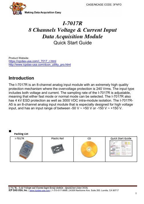
I-7017R - 8-ch Voltage and Current Input DAQ Module - QuickStart (May/2020)ICP DAS USA, Inc. | | 1-310-517-9888 | 24309 Narbonne Ave. Suite 200. Lomita, CA 90717I-7017R8 Channels Voltage & Current InputData Acquisition ModuleQuick Start GuideProduct Website:https:///i_7017_r.html/dcon_utility_pro.htmlIntroductionThe I-7017R is an 8-channel analog input module with an extremely high quality protection mechanism where the overvoltage protection is 240 Vrms. The input type includes both voltage and current. The sampling rate of the I-7017R is adjustable, meaning that either fast mode or normal mode can be selected. The I-7017R also has 4 kV ESD protection as well as 3000 VDC intra-module isolation. The I-7017R-A5 is an 8-channel analog input module that is especially designed for high voltage input, and has an input range of between -50 V ~ +50 V or -150 V ~ +150 V.Packing ListI-7017RPlastic RailCDQuick Start GuideI-7017R - 8-ch Voltage and Current Input DAQ Module - QuickStart (May/2020)ICP DAS USA, Inc. | | 1-310-517-9888 | 24309 Narbonne Ave. Suite 200. Lomita, CA 90717⏹Internal I/O Structure < I-7017R >⏹Pin Assignments < I-7017R, I-7017R >⏹Internal I/O Structure (I-7017R)⏹Modbus Table (M-7017R only)Address Description R/W 10129 ~Over/under range status of channel 0R 10136to 7 for 4 ~ 20mA or 0 ~ 20mA ranges 00129 ~0013630001 ~Analog input value of channel 0 to 7R 3000840001 ~4000840481Firmware version (low word)R 40482Firmware version (high word)R 40483Module name (low word)R 40484Module name (high word)R 40485Module address, valid range: 1 ~ 247R/W 40486Bits 5:0R/WBaud rate, 0x03 ~ 0x0ACode0x030x040x050x06Baud1200240048009600Code0x070x080x090x0ABaud192003840057600115200Bits 7:600: no parity, 1 stop bit01: no parity, 2 stop bit10: even parity, 1 stop bit11: odd parity, 1 stop bit40487Type code R/W Address Description R/W 40488Modbus response delay time in ms,R/W valid range: 0 ~ 3040489Host watchdog timeout value, 0 ~R/W 255, in 0.1s40490Channel enable/disable, 00h ~ FFh R/W 40492Host watchdog timeout count, write 0R/W to clear00257Protocol, 0: DCON, 1: Modbus RTU R/W 00259Filter setting, 0: 60Hz rejection, 1:R/W 50Hz rejection002611: enable, 0: disable host watchdog R/W 00269Modbus data format, 0: hex, 1:R/W engineering00270Host watch dog timeout status, write R/W1 to clear host watch dog timeoutstatus002711: enable, 0: disable fast mode R/W 00273Reset status, 1: first read after R powered on, 0: not the first read afterpowered on⏹DCON ProtocolFunctions Command Response NotesRead module name$AAM!AA(Data)AA: address number Read module firmware version$AAF!AA(Data)Read all analog input data#aa>(data)Read analog input data of each channel (<=16 channel)#aai>(data)i: channel number (Hex) Read analog input data of each channel (>16 channel)#aaii>(data)ii: channel number (Hex) If you want to know the detail DCON protocol, please check it from CD or webCD path: \\napdos\7000\manual\Web: ftp:///pub/cd/8000cd/napdos/7000/manual/I-7017R - 8-ch Voltage and Current Input DAQ Module - QuickStart (May/2020)ICP DAS USA, Inc. | | 1-310-517-9888 | 24309 Narbonne Ave. Suite 200. Lomita, CA 90717I-7017R - 8-ch Voltage and Current Input DAQ Module - QuickStart (May/2020)ICP DAS USA, Inc. | | 1-310-517-9888 | 24309 Narbonne Ave. Suite 200. Lomita, CA 90717⏹Module test and configurationStep 1: INIT switch Operation Step 2: Install & Run DCON Utility 1. Please Install DCON Utility firstYou can find the software in the CD.CD path:<Driver>:\napdos\driver\dcon_utility\Web link:/pub/cd/8000cd/napdos/driver/dcon_utility/ 2. Run DCON utility1. Find out the INIT switch( back of the module),and turn to INIT.2. Reboot the moduleStep 3: Set search configuration & search module Select COM Port Number1. Click “COM Port”2. Assign the communication information and click“OK”Module Default Setting COM Port Refer converter Port Number Baud Rate 9600ProtocolDCON for I-7000Modbus RTU for M-7000Parity Option N,8,13. Click “Search” and select “Start Searching”Software will search the modules from COM Port 4. Click “Search“ and select “stop searching”Manual stop when the modules searchedNote:When no module can be searched, please check the wire and communication informationStep 4: Select Module for testing and configurationDouble click “select module”Step 5: Configuration Settings & Channel SettingsChannel StatusModule SettingsProtocol DCON / ModbusAddress1~255 (0:INIT)Baud rate1200~115200Parity option N,8,1Input range Depends on signalsourcesStep 6: Change to normal mode and keep the settings1.Turn the INIT Switch to Normal.2.Reboot the moduleI-7017R - 8-ch Voltage and Current Input DAQ Module - QuickStart (May/2020)ICP DAS USA, Inc. | | 1-310-517-9888 | 24309 Narbonne Ave. Suite 200. Lomita, CA 90717Trouble ShootingQ1. How to do when forgot module address or baud rate?Please turn to INIT mode, and run DCON Utility to search.The module supports DCON protocol at the INIT mode.And the address is 0. The communication setting is “9600,N,8,1”.Q2. How to configure the I-7000 and M-7000 modules?ICP DAS provide DCON Utility to configure I-7000 and M-7000 modules.Please download the last version from: /pub/cd/8000cd/napdos/driver/dcon_utility/Q3. How to calibrate the analog input module?Usually it is not necessary to calibrate the analog input module.However, in case you need to perform this operation, we provide a function to calibrate the module.Please refer to user manual 1.10.Notice:1.Please update DCON Utility to version 5.2.3 or more.2.Keep the module running more than 30 minutes to warm-up.Q4. How to measure the current?I-7017R and I-7017R require optional external resistance (125Ω) for current measurement.Please refer wired connections diagram.And then select a suitable input range by DCON Utility.Or please use our I-7017RC or I-7017RC modules.Q5. How to programming with I-7000 or M-7000 by C#, VB, VC?ICP DAS I-7000 and M-7000 series both support DCON protocol. And Only M-7000 series supports Modbus protocol.For DCON protocol, please download SDK and Demo from:/pub/cd/8000cd/napdos/driver/dcon_dll_new/For Modbus protocol, please refer this web link:/products/PAC/i-8000/modbus.htmIfthereisanyotherquestion,pleasefeelfreetocontactus.Email:******************Website: /contact_us/contact_us.htmlI-7017R - 8-ch Voltage and Current Input DAQ Module - QuickStart (May/2020)ICP DAS USA, Inc. | | 1-310-517-9888 | 24309 Narbonne Ave. Suite 200. Lomita, CA 90717。

This publication adds the Eight Channel RTD module to the Ovation I/O Reference Manual. It should be placed between Sections 19 and 20.Date: 04/03IPU No.243Ovation ® Interim Publication UpdatePUBLICATION TITLEOvation I/O Reference ManualPublication No. R3-1150Revision 3, March 2003Section 19A. Eight Channel RTDModule19A-1. DescriptionThe Eight (8) channel RTD module is used to convert inputs from Resistance Temperature Detectors (RTDs) to digital data. The digitized data is transmitted to the Controller.19A-2. Module Groups19A-2.1. Electronics ModulesThere is one Electronics module group for the 8 channel RTD Module:n5X00119G01 converts inputs for all ranges and is compatible only with Personality module 5X00121G01 (not applicable for CE Mark certified systems).19A-2.2. Personality ModulesThere is one Personality module groups for the 8 channel RTD Module:n5X00121G01 converts inputs for all ranges and is compatible only with Electronics module 5x00119G01 (not applicable for CE Mark certified systems).19A-2.3. Module Block Diagram and Field Connection WiringDiagramThe Ovation 8 Channel RTD module consists of two modules an electronics module contains a logic printed circuit board (LIA) and a printed circuit board (FTD). The electronics module is used in conjunction with a personalty module, which contains a single printed circuit board (PTD). The block diagram for the 8 channel RTD moduleis shown in Figure 19A-1.Table 19A-1. 8 Channel RTD Module Subsystem ChannelsElectronic Module Personality Module85X00119G015X00121G01Figure 19A-1. 8 Channel RTD Module Block Diagram and Field Connection Wiring Diagram19A-3. SpecificationsElectronics Module (5X00119)Personality Module (5X00121)Table 19A-2. 8 Channel RTD Module SpecificationsDescription ValueNumber of channels8Sampling rate50 HZ mode: 16.67/sec. normally. In 3 wire mode, leadresistance measurement occurs once every 6.45 sec.during which the rate drops to 3/sec.60 HZ mode: 20/sec. normally. In 3 wire mode, leadresistance measurement occurs once every 6.45 sec.during which the rate drops to 2/sec.Self Calibration Mode: Occurs on demand only. The ratedrops to 1/sec. once during each self calibration cycle.RTD ranges Refer to Table 19A-3.Resolution12 bitsGuaranteed accuracy (@25°C)0.10% ±[0.045 (Rcold/Rspan)]% ± [((Rcold + Rspan)/4096 OHM)]% ± [0.5 OHM/Rspan]% ±10 m V ± 1/2LSBwhere:Rcold and Rspan are in Ohms.Temperature coefficient 10ppm/°CDielectric isolation:Channel to channel Channel to logic 200V AC/DC 1000 V AC/DCInput impedance100 M OHM50 K OHM in power downModule power 3.6 W typical; 4.2 W maximumOperating temperature range0 to 60°C (32°F to 140°F)Storage temperature range-40°C to 85°C (-40°F to 185°F)Humidity (non-condensing)0 to 95%Self Calibration On Demand by Ovation ControllerCommon Mode Rejection120 dB @ DC and nominal power line frequency+/- 1/2%Normal Mode Rejection100 dB @ DC and nominal power line frequency+/- 1/2%Table 19A-3. 8 Channel RTD RangesScale #(HEX)Wires Type Tempo FTempo CRcold(ohm)Rhot(ohm)Excitationcurrent(ma)Accuracy± ±countsAccuracy± ±% ofSPAN1310OhmPL0 to1200–18 t o6496106.3 1.090.222310OhmCU 0 to302–18 t o1508.516.5 1.0 130.32D350OhmCU 32 to2840 to1405080 1.0110.2711350OhmCU 32 to2300 to1105378 1.0120.30193100Ohm PL –4 to334–16 t o16892163.671.0110.27223100Ohm PL 32 to5200 to269100200 1.0100.25233100Ohm PL 32 to10400 to561100301 1.0100.25253120Ohm NI –12 t o464–11 t o240109360 1.0100.25263120Ohm NI 32 to1500 to70120170 1.0130.32283120Ohm NI 32 to2780 to122120225 1.0110.27804100Ohm PL 32 to5440 to290100 208 1.0100.25814100Ohm PL 356 t o446180 t o230168 186 1.0300.74824200Ohm PL 32 to6980 to370200 473 1.0120.30834200Ohm PL 514 t o648268 t o342402452 1.0290.71844100Ohm PL 32 to1240 to51100120 1.0190.47854100Ohm PL 32 to2170 to103100 140 1.0130.3286 4100Ohm PL 32 to4120 to211100 180 1.0110.27874100Ohm PL 32 to7140 to379100 240 1.0100.25884120Ohm PL 511 t o662266 t o350200230 1.0240.5919A-4. 8 Channel RTD Terminal Block Wiring Information19A-4.1. Systems Using Personality Module 5X00121G01 Each Personality module has a simplified wiring diagram label on its side, which appears above the terminal block. This diagram indicates how the wiring from the field is to beconnected to the terminal block in the base unit. The following table lists and defines the abbreviations used in this diagram.Table 19A-4. Abbreviations Used in the DiagramAbbreviation Definition+IN, -IN Positive and negative sense input connectionEarth ground terminal. Used for landing shields when the shield is to begrounded at the module.PS+, PS-Auxiliary power supply terminals.RTN Return for current source connection.SH Shield connector. used for landing shields when the shield is to begrounded at the RTD.SRC Current source connection.Note:PS+ and PS- are not used by this module.19A-5. 8 Channel RTD Module Address Locations19A-5.1. Configuration and Status RegisterWord address 13 (D in Hex) is used for both module configuration and module status. The Module Status Register has both status and diagnostic information. The bit information contained within these words is shown in Table 19A-5.Definitions for the Configuration/Module Status Register bits:Bit 0:This bit configures the module (write) or indicates the configuration state of the module (read). A “1” indicates that the module is configured. Note that until the module is configured, reading from addresses #0 through #11 (B in Hex) will produce an attention status.Bit 1:This bit (write “1”) forces the module into the error state, resulting in the error LED being lit. The read of bit “1” indicates that there is an internal module error,or the controller has forced the module into the error state. The state of this bit is always reflected by the module’s Internal Error LED. Whenever this bit is set,an attention status is returned to the controller when address #0 through #11(B in Hex) are read.Table 19A-5. 8 Channel RTD Configuration/Status Register (Address 13 0xD in Hex)Bit Data Description -Configuration Register (Write)Data Description -Status Register (Read)0Configure Module Module Configured(1 = configured; 0 = unconfigured)1Force errorInternal or forced error(1 = forced error; 0 = no forced error)250/60 Hz select (0 = 60Hz, 1 = 50Hz)50/60 Hz System (1 = 50Hz) d(read back)3SELF_CAL (Initiates Self Calibration)Warming bit (set during power up or configuration)40050060Module Not Calibrated 708CH.1 _ 3/4 Wire.CH.1 _ 3/4 Wire - Configuration (read back)9CH.2 _ 3/4 Wire.CH.2 _ 3/4 Wire - Configuration (read back)10CH.3 _ 3/4 Wire.CH.3 _ 3/4 Wire - Configuration (read back)11CH.4 _ 3/4 Wire.CH.4 _ 3/4 Wire - Configuration (read back)12CH.5 _ 3/4 Wire.CH.5 _ 3/4 Wire - Configuration (read back)13CH.6 _ 3/4 Wire.CH.6 _ 3/4 Wire - Configuration (read back)14CH.7 _ 3/4 Wire.CH.7 _ 3/4 Wire - Configuration (read back)15CH.8 _ 3/4 Wire.CH.8 _ 3/4 Wire - Configuration (read back)Bit 2:The status of this bit (read) indicates the conversion rate of the module, write to this bit configures the conversion rate of A/D converters as shown below.see Table 19A-6.Bit3:Write: This bit is used to initiate self-calibration. Read: This bit indicates that the module is in the “Warming” state. this state exists after power up and ter-minates after 8.16 seconds. the module will be in the error condition during the warm up period.Bit4 & 5:These bits are not used and read as “0” under normal operation.Bit 6:This bit (read) is the result of a checksum test of the EEPROM. A failure of this test can indicate a bad EEPROM, but it typically indicates that the module has not been calibrated. A “0” indicates that there is no error condition. If an error is present, the internal error LED is lit and attention status will be returned for all address offsets 0-11 (0x0 - 0xB). The “1” state of this bit indicates an unre-coverable error condition in the field.Bit 7:This bits is not used and read as “0” under normal operation.Bit 8 - 15:These bits are used to configure channels 1 - 8 respectively for 3 or 4 wire op-eration. A “0” indicates 3 wire and a “1” indicates 4 wire operation, see Table 19A-7 and Table 19A-8).Word address 12 (0xC) is used to configure the appropriate scales for Channels 1 - 4 (refer to Table 19A-7 and Table 19A-8).Table 19A-6. Conversion Rate Conversion Rate (1/sec.)Bit 260 (for 60Hz systems)050 (for 50Hz systems)1Table 19A-7. Data Format for the Channel Scale Configuration Register(0xC)Bit Data Description Configuration (Write)Data Description Status (Read)0 Configure Channel #1scale - Bit 0Channel #1 scale configuration (read back) - Bit 01Configure Channel #1scale - Bit 1Channel #1 scale configuration (read back) - Bit 12Configure Channel #1scale - Bit 2Channel #1 scale configuration (read back) - Bit 23Configure Channel #1scale - Bit 3Channel #1 scale configuration (read back) - Bit 34Configure Channel #2 scale - Bit 0Channel #2 scale configuration (read back) - Bit 05Configure Channel #2 scale - Bit 1Channel #2 scale configuration (read back) - Bit 16Configure Channel #2 scale - Bit 2Channel #2 scale configuration (read back) - Bit 27Configure Channel #2 scale - Bit 3Channel #2 scale configuration (read back) - Bit 38Configure Channel #3 scale - Bit 0Channel #3 scale configuration (read back) - Bit 09Configure Channel #3 scale - Bit 1Channel #3 scale configuration (read back) - Bit 1Caution:Configuring any or all channel scales while the system is running will cause all channels to return attention status for up to two seconds following the reconfiguration.Caution:Configuring any or all channel scales while the system is running will cause all channels to return attention status for up to two seconds following the reconfiguration.10Configure Channel #3 scale - Bit 2Channel #3 scale configuration (read back) - Bit 211Configure Channel #3 scale - Bit 3Channel #3 scale configuration (read back) - Bit 312Configure Channel #4 scale - Bit 0Channel #4 scale configuration (read back) - Bit 013Configure Channel #4 scale - Bit 1Channel #4 scale configuration (read back) - Bit 114Configure Channel #4 scale - Bit 2Channel #4 scale configuration (read back) - Bit 215Configure Channel #4 scale - Bit 3Channel #4 scale configuration (read back) - Bit 3Table 19A-8. Data Format for the Channel Scale Configuration Register(0xE)Bit Data Description Configuration (Write)Data Description Status (Read)0 Configure Channel #5 scale - Bit 0Channel #5 scale configuration (read back) - Bit 01Configure Channel #5 scale - Bit 1Channel #5 scale configuration (read back) - Bit 12Configure Channel #5 scale - Bit 2Channel #5 scale configuration (read back) - Bit 23Configure Channel #5 scale - Bit 3Channel #5 scale configuration (read back) - Bit 34Configure Channel #6 scale - Bit 0Channel #6 scale configuration (read back) - Bit 05Configure Channel #6 scale - Bit 1Channel #6 scale configuration (read back) - Bit 16Configure Channel #6 scale - Bit 2Channel #6 scale configuration (read back) - Bit 27Configure Channel #6 scale - Bit 3Channel #6 scale configuration (read back) - Bit 38Configure Channel #7 scale - Bit 0Channel #7 scale configuration (read back) - Bit 09Configure Channel #7 scale - Bit 1Channel #7 scale configuration (read back) - Bit 110Configure Channel #7 scale - Bit 2Channel #7 scale configuration (read back) - Bit 211Configure Channel #7 scale - Bit 3Channel #7 scale configuration (read back) - Bit 312Configure Channel #8 scale - Bit 0Channel #8 scale configuration (read back) - Bit 013Configure Channel #8 scale - Bit 1Channel #8 scale configuration (read back) - Bit 114Configure Channel #8 scale - Bit 2Channel #8 scale configuration (read back) - Bit 215Configure Channel #8 scale - Bit 3Channel #8 scale configuration (read back) - Bit 3Table 19A-7. Data Format for the Channel Scale Configuration Register(0xC)19A-6. Diagnostic LEDsTable 19A-9. 8 Channel RTD Diagnostic LEDsLED DescriptionP (Green)Power OK LED. Lit when the +5V power is OK.C (Green)Communications OK LED. Lit when the Controller is communicatingwith the module.I (Red)Internal Fault LED. Lit whenever there is any type of error with themodule except to a loss of power. Possible causes are:n - Module initialization is in progress.n - I/O Bus time-out has occurred.n - Register, static RAM, or FLASH checksum error.n - Module resetn - Module is uncalibrated.n - Forced error has been received from the Controllern - Communication between the Field and Logic boards failedCH1 - CH 8 (Red)Channel error. Lit whenever there is an error associated with a channel or channels. Possible causes are:n - Positive overrangen - Negative overrangen Communication with the channel has failed。
简单i o口扩展实验报告简单I/O口扩展实验报告引言在现代科技发展的浪潮下,电子设备的功能和复杂性不断提升。
然而,对于初学者来说,了解和掌握电子设备的基本原理和操作方法是非常重要的。
本实验旨在通过简单的I/O口扩展实验,帮助初学者更好地理解和应用I/O口扩展技术。
一、实验目的本实验的主要目的是通过使用I/O口扩展技术,实现电子设备与外部设备的交互功能。
具体目标包括:1. 了解I/O口扩展的基本原理和应用场景;2. 学习使用I/O口扩展芯片进行输入输出控制;3. 实现简单的电子设备与外部设备的交互功能。
二、实验器材1. Arduino开发板;2. I/O口扩展芯片;3. 电阻、电容等基本电子元件;4. 连接线、面包板等实验工具。
三、实验步骤1. 连接电路将Arduino开发板与I/O口扩展芯片通过连接线连接起来,按照电路图进行正确的连接。
确保电路连接无误后,将其连接到电源。
2. 编写程序在Arduino开发环境中,编写程序以实现所需的输入输出控制功能。
通过调用相应的库函数,配置I/O口扩展芯片的输入输出模式,并编写相应的逻辑控制代码。
3. 烧录程序将编写好的程序烧录到Arduino开发板中,确保程序能够正确运行。
4. 实验验证运行程序后,通过操作外部设备,如按钮、LED灯等,验证I/O口扩展功能的正确性。
观察外部设备的状态变化,以及Arduino开发板的响应情况。
四、实验结果与分析通过实验,我们成功实现了I/O口扩展技术的应用。
通过编写程序,我们可以根据需要配置I/O口扩展芯片的输入输出模式,并通过控制逻辑实现与外部设备的交互功能。
在实验过程中,我们发现通过I/O口扩展技术,可以实现大量的输入输出控制。
例如,我们可以通过按钮控制LED灯的开关,通过传感器获取环境温度并进行相应的控制,通过继电器控制电机等。
这些功能的实现,不仅提高了电子设备的灵活性和可扩展性,也为我们提供了更多的创造空间。
然而,我们也发现在实际应用中,I/O口扩展技术还存在一些挑战和限制。
CCS3.3中常见问题解决(待续)(2013-05-22 18:05:59)转载▼问题1:用CCS3.3编译时出现“entry point other than _c_int00 specified”的错误的问题解决出现的错误如下:[Linking...] \"D:\\CCStudio_v3.1\\C2000\\cgtools\\bin\\cl2000\" -@\"Debug.lkf\">> warning: entry point other than _c_int00 specifiedBuild Complete,0 Errors, 1 Warnings, 0 Remarks.此错误在Autoinit Model:Project>Build Options…>Linker>Basic选择Run-Time Autoinitialization不变,只需把Code Entry Point:项的code_start 改为:c_int0问题2:用CCS3.3编译时出现“last line of file ends without a newline”的错误的问题解决出现的错误如下:"expFile.c", line 7: warning: last line of file ends without a newline[Linking...] "C:\CCStudio_v3.3\C2000\cgtools\bin\cl2000" -@"Debug.lkf"Build Complete,0 Errors, 1 Warnings, 0 Remarks.此错误在程序.C代码的最后一行打几个回车问题3:用CCS3.3编译时出现“linking files with incompatible memory models (*\\rts2800.lib', member'args_main.obj')”的错误的问题解决出现的错误如下:>> error: linking files with incompatible memory models (library 'C:\\CCStudio_v3.3\\C2000\\cgtools\\lib\\rts2800.lib', member 'args_main.obj')>> Compilation failureBuild Complete,n Errors, 0 Warnings, 0 Remarks.此错误将库文件rts2800.lib移除(右击rts2800.lib>Remove from projet),然后添加rts2800_ml.lib库(右击Libraries>Add Files to project...>CCstdio_v3.3\C2000\cgtools\librts2800_ml.lib)。
KFD2-SR2-Ex1.W06.03.2002Transformer Isolated BarriersOutput: RelayTechnical dataKFD2-SR2-Ex1.W103367_e n g06.03.2002Power supply Connection typePower Rail or terminals 14+, 15-Rated operational voltage 20 ... 30 V DC Rated operational current 20 ... 23 mA Safety maximum voltage U m 40 V DC Ripple£ 10 %Input (intrinsically safe)Connection type terminals 1+, 2+, 3-Nominal datain accordance with IEC 60947-5-6 (NAMUR, DIN 19234); see system description for electrical dataQuiescent voltage/Short-circuit current approx. 8 V DC / approx. 8 mA Switching point/Switching hysteresis 1.2 ... 2.1 mA / approx. 0.2 mA Input pulse length/Input pulse interval Š 20 ms / Š 20 msLead monitoringbreakage J £ 0.1 mA , short-circuit J > 6 mADetails of certificate of conformity Certification numberPTB 00 ATEX 2080 ; for additional certifications refer to the approval list Group, category, ignition protection method¬ II (1) G D [EEx ia] IIC Voltage U 010.5 V Current I 013 mA PowerP 034 mWAllowable circuit valuesIgnition protection class, category [EEx ia and EEx ib]Explosion groupIIA IIB IIC External capacitance 75 µF 16.8 µF 2.41 µF External inductance1000 mH 840 mH 210 mH Entity parameter Certification number J.I.3002773FM control drawingNo. 116-0035Suitable for installation in division 2 yesConnection type terminals 1, 3; 2, 3; 4, 6; 5, 6Input IVoltage V OC12.9 V Current I SC19.8 mAExplosion groupA&B C&E D, F&G Max. external capacitance C a 1.273 µF 3.82 µF 10.18 µF Max. external inductance L a84.8 mH 254.4 mH 678.4 mH Safety parameter UL control drawing E 106378CSA control drawing LR 36087-13Control drawing No. 116-0047Connection type terminals 1, 3; 2, 3; 4, 6; 5, 6Input ISafety parameter 12.6 V / 650 Ohm Voltage V OC12.9 V Current I SC19.8 mAExplosion groupA&B C&E D, F&G Max. external capacitance C a 1.273 µF 3.82 µF 10.18 µF Max. external inductance L a84.88 mH 298.7 mH 744.4 mHOutput (not intrinsically safe)Connection type terminals 7, 8, 9Outputsignal ; relayContact loading253 V AC / 2 A / cos j > 0.7; 40 V DC / 2 A ohmic load; from january 2002 increase of the con-tact rating to 4A for 115 V AC switching voltage. The respective connection data are shown on the type plate.Mechanical life107 switchingsEnergized/De-energized delay approx. 20 ms / approx. 20 ms Transfer characteristics Switching frequency < 10 HzGalvanic isolation Input/Outputsafe galvanic isolation acc. to EN 50020, voltage peak value 375 V Input/Power supplysafe galvanic isolation acc. to EN 50020, voltage peak value 375 V103367_e n g 06.03.2002Output/Power supply safe isolation acc. to DIN VDE 0106, design isolation voltage 253 V eff Ambient conditions Ambient temperature -20 ... 60 °C (253 ... 333 K)Standard conformity Inputin accordance with IEC 60947-5-6 (NAMUR, DIN 19234); see system description for electrical dataCoordination of insulation accord. to DIN EN 50178Galvanic isolation accord. to DIN EN 50178Climatic conditionsaccord. to DIN IEC 721Electromagnetic compatibility accord. to EN 50081-2 / EN 50082-2, NAMUR NE 21Mechanical specifications Massapprox. 150 gPower Rail PR 05Power Rail UPR 05Power feed module KFD2-EB2The devices are supplied with 24 V DC due to the power feed module KFD2-EB2 and via the Power Rail PR 05 or UPR 05, simultaneously the combined fault indication will be evaluated.Each power feed module serves the fusing and monitoring of groups with up to 100 single devices. The PR 05 Power Rail is an inset component for the DIN rail. The UPR 05 Power Rail is a complete unit consisting of the electrical insert and an aluminum 35 x 15 x 2000 mm DIN rail.Devices are simply snapped onto it for an electrical connection.Without the use of a Power Rail, the power supply to the device is directly through the device terminals.Accessories:103367_e n g 06.03.2002。
Simulator for Z80+ Release 09.2023TRACE32 Online HelpTRACE32 DirectoryTRACE32 IndexTRACE32 Documents ......................................................................................................................TRACE32 Instruction Set Simulators ..........................................................................................Simulator for Z80+ (1)TRACE32 Simulator License (4)Quick Start of the Simulator (5)Peripheral Simulation (7)Troubleshooting (8)FAQ (8)Emulation Modes (9)SYStem.Mode Establish the communication with the simulator9 SYStem.CPU CPU type10General SYStem Settings and Restrictions (11)SYStem.Option.BASE Base address of internal registers11Using the MMU for Z180 (12)Memory Classes (14)Version 10-Oct-2023All general commands are described in the “PowerView Command Reference” (ide_ref.pdf) and “General Commands Reference”.TRACE32 Simulator License[build 68859 - DVD 02/2016] The extensive use of the TRACE32 Instruction Set Simulator requires a TRACE32 Simulator License.For more information, see /sim_license.html.Quick Start of the SimulatorTo start the simulator, proceed as follows:1.Select the device prompt for the Simulator and reset the system.The device prompt B:: is normally already selected in the TRACE32 command line . If this is not the case, enter B:: to set the correct device prompt. The RESet command is only necessary if you do not start directly after booting TRACE32.2.Specify the CPU specific settings.The default values of all other options are set in such a way that it should be possible to work without modification. Please consider that this is probably not the best configuration for your target.B::RESetSYStem.CPU <cpu_name>3.Enter debug mode.SYStem.UpThis command resets the CPU and enters debug mode. After this command is executed it is possible to access memory and registers.4.Load the program.Data.LOAD.<file_format> <file>; load program and symbols See the Data.LOAD command reference for a list of supported file formats. If uncertain about the required format, try Data.LOAD.auto.A detailed description of the Data.LOAD command and all available options is given in the referenceguide.5.Start-up exampleA typical start sequence is shown below. This sequence can be written to a PRACTICE script file(*.cmm, ASCII format) and executed with the command DO<file>.B::; Select the ICD device promptWinCLEAR; Clear all windowsSYStem.CPU <cpu_name>; Select CPU typeSYStem.Up; Reset the target and enter; debug modeData.LOAD.<file_format> <file>; Load the applicationRegister.Set pc main; Set the PC to function mainPER.view; Show clearly arranged; peripherals in window *) List.Mix; Open source code window *)Register.view /SpotLight; Open register window *)Frame.view /Locals /Caller; Open the stack frame with; local variables *) Var.Watch %Spotlight flags ast; Open watch window for; variables *) *) These commands open windows on the screen. The window position can be specified with the WinPOS command.Peripheral SimulationFor more information, see “API for TRACE32 Instruction Set Simulator” (simulator_api.pdf).TroubleshootingNo information available.FAQPlease refer to https:///kb.Emulation ModesSYStem.Mode Establish the communication with the simulatorFormat:SYStem.Mode <mode>SYStem.Down (alias for SYStem.Mode Down)SYStem.Up (alias for SYStem.Mode Up)<mode>:DownNoDebugGoUpDefault: Down.Selects the target operating mode.Down The CPU is in reset. Debug mode is not active. Default state and state after fatalerrors.NoDebug The CPU is running. Debug mode is not active. Debug port is tristate. In thismode the target should behave as if the debugger is not connected.Go The CPU is running. Debug mode is active. After this command the CPU can bestopped with the break command or if any break condition occurs.Up The CPU is not in reset but halted. Debug mode is active. In this mode the CPUcan be started and stopped. This is the most typical way to activate debugging.If the mode Go is selected, this mode will be entered, but the control button in the SYStem.state window jumps to the mode Up.SYStem.CPU CPU type Format:SYStem.CPU <mode><mode>:Z80 | Z180 | Z181 | Z182Selects the processor type. The ROM debugger requires also a modification in the debug monitor fordifferent processor types.General SYStem Settings and RestrictionsSYStem.Option.BASE Base address of internal registers Format:SYStem.Option.BASE <address>Defines the base address of the internal registers.Using the MMU for Z180This command and the commands MMU support the built-in MMU of the Z180 processors.The analyzer and all memory systems and breakpoints are based on the physical address. The display in the analyzer can be both physical or logical addresses. A logical address can have two formats: smaller than 64K or larger. Smaller addresses are assumed to be an logical address as seen by the CPU in the current MMU configuration. If an address is larger than 64K, the address bits A16 to A23 define the bank base address used for the BBR or CBR register. Logical above 64K addresses should only be used, if the MMU registers were already setup. The following schematic shows these relations for some examples:preset: CBAR=84,BBR=10, CBR=20logical address:504567(Hex)16 bitCBR/BBR =50logical CPU address-->physical address:54567logical address:001567(Hex)16 bitcurrent-mmu logical CPU address-->physical address:1567logical address:004567(Hex)16 bitcurrent-mmu logical CPU address-->MMU Bank Area-->physical address:04567+BBR10---=14567logical address:00c d e f(Hex)16 bitcurrent-mmu logical CPU address-->COMMON1 Area-->physical address:0cdef+CBR+20---=2cdefT o activate the correct address translation for breakpoints, the MMU command must be activated. The following example loads a banked application:mmu.offmap.rom 0x0--0x7ffff…mmu.ond.load.u iarz180.dbgThe next example loads a banked application in two logical units:CBAR=84, CBR=0, BBR=10 or 20mmu.resetsymbol.resetmap.rom 0x--0x7ffff…mmu.create 0x104000--0x107fffmmu.create 0x204000--0x207fffmmu.ond.load.b bank1.cod 0x104000 /nosymbold.load.b bank2.cod 0x204000 /nosymbold.load.b common.cod 0x2000 /nosymbold.load.sym bank1.sym /noclearsymbol.reloc p:100000 0x4000--0x4fffd.load.sym bank2.sym /noclearsymbol.reloc p:200000 0x4000--0x4fffd.load.sym common.sym /noclearMemory ClassesMemory Class DescriptionD DataP ProgramC Memory access by CPUE Emulation memory accessA Absolute (physical) memory access。
Technical Data Sheet
Additin®RC 2317EP Additive
Type EP additive; light coloured, low odoured, low viscosity, active sulphur carrier
Technical Data Composition
Appearance
Colour (ASTM-D 1500)
Sulphur
Active sulphur (ASTM-D 1662)
Copper corrosion (ASTM-D 130)
5 % weight Additin RC 2317 in a
paraffinic base oil, 3 h/100 °C
Viscosity, 40°C (ASTM-D 445)
Density, 20°C (ASTM-D 1298)
Flash point, COC (ASTM-D 92)sulphurized vegetable fatty acid esters, mineral oil-free
light brown, clear, low viscosity liquid typ. 4.5
approx. 17 % weight
approx. 8 % weight
3a - 3b
approx. 55 mm²/s
approx. 1.01 g/ml
> 180°C
Application- medium and heavy duty cutting oils
- deep hole drilling oils
- honing oils
- grinding oils
- broaching oils
Additin RC 2317 is a light-coloured, near odourless, low viscosity sulphur
carrier. It is used for manufacturing metalworking fluids for cutting operations.
Due to its low viscosity Additin RC 2317 is ideally suited for formulating
metalworking fluids such as deep hole drilling and honing oils from which an
excellent flushing effect is required. By virtue of specially selected raw material
Additin RC 2317 exhibits a very low pourpoint and extended solubility in various
base fluids compared to conventional sulphur carriers. Therefore Additin RC
2317 is ideally suited for metalworking oils based on hydrocrack oils.
The performance of metalworking fluids containing Additin RC 2317 can be
increased by combination with zinc dithiophosphates, e.g. Additin RC 3038,
phosphoric acid partial esters or ashless phosphorus-sulphur additives e.g.
RC 3880.
Solubility Soluble in mineral oils and synthetic base oils. However, it is necessary to
verify the solubility in the base oils used and the compatibility with other
additives.
Test Results
Paraffinic base oil,ISO VG
ISO VG 15
base oil,
no additives +2%b.w.
RC
RC 2317
+5%b.w.
RC
RC 2317
+10
10 %b.w.
RC
RC 2317
+15
15 %b.w.
RC
RC 2317
Four-ball test
(DIN 51350, part 2)
weld load600 - 700 N1800 - 2000 N2000 - 2200 N2800 - 3000 N3200 - 3400 N Four-ball test
(DIN 51350, part 3)
scar diameter
1h/300N
0.70 mm0.50 mm0.60 mm0.63 mm0.75 mm
Four-ball test
(ASTM D-2783)
weld point LWI 200 kg
38 kg
250 kg
42 kg
Load-carrying test
according to Brugger
load capacity< 20 N/mm²approx.
45 N/mm²
approx.
60 N/mm²
approx.
85 N/mm²
approx.
95 N/mm²
Packing Unit200 kg bunghole drums
Storage Conditions In a dry place at room temperature approx. 12 months.
Handling Consult material safety data sheet (MSDS)
for additional handling information on Additin RC 2317.
® = registered trade mark * The analytical data are
guide values. Additin RC 2317 is on EINECS and
TSCA inventory.
Version: 1/12. Dec 2000
Our technical advice - whether verbal, in writing or by way of trials - is given in good faith but without warranty, and this also applies where proprietary rights of third parties are involved. It does not release you from the obligation to test the products supplied by us as to their suitability
for the intended processes and uses. The
application, use and processing of the
products are beyond our control and,
therefore, enti- rely your own responsibility.
Should, in spite of this,
liability be established for any damage, it
will be limited to the value of the goods
delivered by us and used by you. We will, of
course, provide products of consistent
quality within the scope of our General
Conditions of Sale and Delivery.
Rhein Chemie Rheinau GmbH Duesseldorfer Strasse 23-27 68219 Mannheim, Germany Tel.: +49-621-8907-0
Fax: +49-621-8907-675
E-Mail: @。