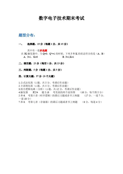
电子科技大学,数字电路 期末总复习提纲
- 格式:pdf
- 大小:705.74 KB
- 文档页数:21
1.PPT
2.
3.
Chapter 2 Number Systems and Codes
1)decimal binary octal and hexadecimal numbers
and their conversion one another.
2addition and subtraction of nondecimal numbers
R R
Chapter 2 Number Systems and Codes
3signed binary numbers signed-magnitude system two s-complement one s-complement and their conversion one
another; two s-complement addition and
subtraction
3
3
1.
1
3signed binary numbers signed-magnitude system two s-complement one s-complement and their conversion one
another; two s-complement addition and
subtraction
Chapter 2 Number Systems and Codes 4) binary codes for decimal numbers(BCD), Gray
Code,and the conversions between them and binary numbers.
8421BCD3
8421BCD
BCD
3
?
Chapter 3 Digital Circuits 1.
2.CMOS
1
2CMOS
3
4
5
6) CMOS
Chapter 4 Combinational Logic Design Principles
1.
2.
--
3.
4.
Chapter 4 Combinational Logic Design Principles
5 .
6.
7.
Chapter 6 Combinational Logic Design Practices 1.
2.MSI2-474x139
74x13874x49 74x148
74x151
3.
4.
5. MSI
Chapter 7 Sequential Logic Design Principles
1.D J-K T
2.
Mealy Moore
3.
1Determine the next-state functions F (excitation equations) and output functions G. F(
G
2To get the next state equation of Q* (transition equations) by using flip-flop s characteristic equation.
F Q*,
3To produce transition/output table and state/output table by using transition equations and output equations.
// 4Plot out state diagram and timing diagram. ( optional)
5Check circuit whether it is self-correcting.
6Describe circuit s function.
4.
1construct a original state/output table or state diagram corresponding to the word description or specification.
/
2minimize original state/output table. and plot out the minimized state/out table.
(/
/
4.
3choose a set of state variables and assign state-variable combinations to the named states coded
state
4create a transition/output table.
//
5write out the transition equations and output equation.
/
6)choose a flip-flop type.
D J-K
4.
7derive the excitation equations.
method derive the excitation equations according to transition equations and characteristic equation. )
8draw a logic circuit diagram corresponding to the excitation equations and output equations.
9the disposition of unused states:
minimal risk: self-correcting circuit
minimal cost: don t-care terms, simplify the circuit.
4.
Chapter 8 Sequential Logic Design Practices
1. :
1
2SSI (D JK T
3MSI : 74X16374X16174X16074X162 ,74X169 4MSI
Chapter 8 Sequential Logic Design Practices
2. :
MSI : 74X16474X16674X19474X299
3.
1ring counters n
2Johnson counters n
3MSI ( 74X194
Chapter 8 Sequential Logic Design Practices
Chapter 8 Sequential Logic Design Practices
5.
1SSI D JK
274X194
374X194
Chapter 9 Memory (
1. to know about the basic principles of ROM
SRAM and their structures
ROM,SRAM
2. to grip memory s application in digit system hardware realization
3.
4. ROM
5.
This document was created with Win2PDF available at . The unregistered version of Win2PDF is for evaluation or non-commercial use only. This page will not be added after purchasing Win2PDF.。