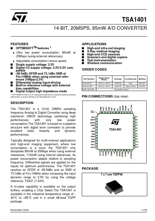
1/19FEATURESsOPTIMWATT TM features 1lUltra low power consumption: 85mW at 20Msps (using external references).lAdjustable consumption versus speed.s Single supply voltage: 2.5Vs Digital I/O supply voltage: 2.5V/3.3V com-patibles -90.5dBc SFDR and 73.1dBc SNR at Fin=10MHz when using external refer-ences (VINpp=2.5V)s Differential analog input-drivings Built-in reference voltage with external bias capabilitiessDigital output high impedance mode1) OPTIMWATT(TM) is a ST deposited trademark for products features allowing optimization of power efficiency at chip/application level.DESCRIPTIONThe TSA1401 is a 14-bit, 20MHz sampling frequency Analog to Digital Converter using deep submicron CMOS technology combining high performances with very low power consumption.The TSA1401 is based on a pipeline structure with digital error correction to provide excellent static linearity and dynamic performances.Typically designed for multi-channel applications and high-end imaging equipment, where low consumption is a must, the TSA1401 only dissipates 85mW at 20Msps when using external references, 110mW using internal references. Its power consumption adapts relative to sampling frequency. Differential signals are applied on the inputs for optimum performance. The TSA1401reaches an SFDR of -90.5dBc and an SNR of 73.1dBc at Fin=10MHz when increasing the input dynamic range to 2.5V by using the voltage reference, TS431 (1.24V).A tri-state capability is available on the output buffers, enabling a Chip Select.The TSA1401 is available in the industrial temperature range of -40°C to +85°C and in a small 48-lead TQFP package.APPLICATIONSs High-end infra-red imaging s X-Ray medical imaging s High-end CCD camerass Scanners and digital copiers s Test instrumentation sWireless communicationORDER CODESPIN CONNECTIONS (top view)PACKAGEPart Number Temperature Range Package ConditioningMarking TSA1401IF -40°C to +85°C TQFP48Tray SA1401TSA1401IFT -40°C to +85°CTQFP48Tape & ReelSA1401EVAL1401/ABEvaluation boardTSA1401TSA140114-BIT, 20MSPS, 85mW A/D CONVERTER1/19December 2003TSA1401ABSOLUTE MAXIMUM RATINGS1 ABSOLUTE MAXIMUM RATINGSOPERATING CONDITIONS BLOCK DIAGRAMSymbolParameterValuesUnitAVCC, DVCC, VCCBI Analog, digital, digital buffer Supply voltage 11)All voltage values, except differential voltage, are with respect to network ground terminal. The magnitude of input and output voltages must not exceed -0.3V or VCC -0.3V to 3.3V V VCCBEDigital buffer Supply voltage 10V to 3.6V V VIN, VINB, VREFP, VREFM, VINCM Analog inputs-0.3V to AVCC+0.3V V IDout Digital output current -100mA to 100mAmA Tstg Storage temperature+150°C ESDElectrical Static Discharge - HBM: Human Body Model 2- CDM-JEDEC Standard2)ElectroStatic Discharge pulse (ESD pulse) simulating a human body discharge of 100 pF through 1.5k Ω2000700VLatch-upClass 33)ST Microelectronics Corporate procedure number 0018695ASymbolParameterTest conditions MinTypMaxUnitAVCC Analog Supply voltage 2.25 2.5 2.7V DVCC Digital Supply voltage 2.25 2.5 2.7V VCCBI Digital buffer Supply voltage 2.25 2.5 2.7V VCCBEDigital buffer Supply voltage2.252.53.3VIPOL VREFMVREFP CLKVIN VINBDFSB OEBDR DOTO D13ORINCM GNDAREFMODEABSOLUTE MAXIMUM RATINGSTSA1401PIN DESCRIPTIONS Pin Name I/ONoPin DescriptionIPOL I1Analog bias current input - adjusts polarization current versus Fs.VREFP I/O 2Top Reference Voltage - may be used as a voltage generator output or used as aninput to adjust the input dynamic range (VIN-VINB=2x(VREFP-VREFM)).VREFM I 3Bottom Reference Voltage. Usually connected to GND (see AN p12 for details)AGND I 4, 6, 8, 10, 48Analog ground.VIN I 5Positive Analog input.VINB I 7Negative Analog Input.INCM I/O 9Internal Common Mode - may be used as a voltage generator output for input sig-nal common mode or used as an input to force the internal common mode (see ANp12 for more details).AVCC I 11, 12, 46, 47Analog Power Supply (2.5V).DVCC I 13, 14Digital Power Supply (2.5V) (Clock).DGND I 15, 17,19Digital Ground (Clock).CLK I 16CMOS Clock Input.NC NA 18, 42Non Connected Pin.GNDBI I 20Digital Ground (Internal Buffer).GNDBE I 21,40Digital Ground (External Buffer).VCCBE I 22, 39Digital Power Supply (External Buffer, 2.5V/3.3V).OR O 23Over Range Indicator, if D0-D13=’1’ or ‘0’, OR=’1’.D13(MSB)-D0(LSB)O 24-37Data CMOS Outputs (2.5V/3.3V).DR O 38Data Ready Signal (2.5V/3.3V).VCCBI I 41Digital Power Supply (Internal Buffers 2.5V).REFMODE I 43REFMODE=’VIL’, internal references active.REFMODE=‘VIH’, external references must be applied.OEB I 44Output Enable Input. If OEB=’VIH’ then D0-D13 in ‘High Z’ state.DFSBI45Data Format Select Input - If DFSB=’VIH’ then D13 is standard binary output cod-ing; if DFSB=’VIL’ then D13 is two’s complemented.TSA1401ELECTRICAL CHARACTERISTICS2 ELECTRICAL CHARACTERISTICSAVCC = DVCC = VCCBI =VCCBE = 2.5V, Fs= 20MHz, Fin= 10MHz, VIN-VINB@ -1.0dBFS, VREFM=0V, VREFP=1V, INCM=0.5V (external references), Tamb = 25°C (unless otherwise specified)Timing CharacteristicsTiming DiagramSymbolParameterTest conditions MinTyp MaxUnitFS Sampling Frequency 0.520MHz DC Clock Duty Cycle 50%TC1Clock pulse width (high)25ns TC2Clock pulse width (low)25nsTod Data Output Delay (Fall of Clock to Data Valid)10pF load capacitance 67.511ns Tpd Data Pipeline delay8.5cycles Ton Falling edge of OEB to digital output valid data1ns ToffRising edge of OEB to digital output tri-state1nsELECTRICAL CHARACTERISTICS TSA1401Dynamic CharacteristicsAccuracyAnalog InputsInternal Reference VoltageSymbolParameter Test conditionsMin TypMaxUnitSFDR 1Spurious Free Dynamic Range Fin=10MHz, VREFP=1VFin=10MHz, VREFP=1.24V (TS431)Fin=10MHz, internal references-89-91.5-91-74dBFSSNR 1Signal to Noise Ratio Fin=10MHz, VREFP=1VFin=10MHz, VREFP=1.24V (TS431)Fin=10MHz, internal references6871.573.170dBcTHD 1Total Harmonic Distortion Fin=10MHz, VREFP=1VFin=10MHz, VREFP=1.24V (TS431)Fin=10MHz, internal references-85-85.9-86-71dBcSINAD 1Signal to Noise and Distortion RatioFin=10MHz, VREFP=1V Fin=10MHz, VREFP=1.24V (TS431)Fin=10MHz, internal references667172.8569.9dBcENOB 1Effective Number of BitsFin=10MHz, VREFP=1VFin=10MHz, VREFP=1.24V (TS431)Fin=10MHz, internal references10.911.71211.5bits1)Typical values have been measured using the evaluation board on a dedicated test bench.SymbolParameter Min TypMax UnitOE Offset Error -3LSB GE Gain Error0.04%DNL Differential Non Linearity ±0.8LSB INL Integral Non Linearity±2LSB-Monotonicity and no missing codesGuaranteedSymbolParameterTest conditions Min TypMax Unit VIN-VINB Analog Input Voltage, Differential 2Vpp Cin Analog Input capacitance 4.0pF Zin Analog Input impedance Fs=20MHz3.3k ΩBWAnalog Input Bandwidth (-3dB)Full power, VIN-VINB=2.0Vpp, Fs=20MHz1000MHzTSA1401ELECTRICAL CHARACTERISTICSExternal Reference VoltagePower ConsumptionRrefOReference output impedanceREFMODE=’0’: int references18.7ΩSymbolParameterTest conditionsMin TypMax UnitSymbolParameterTest conditionsMinTyp MaxUnitVREFP Forced Top reference voltage REFMODE=’1’0.8 1.3V VREFM Bottom reference voltage 00.2V VINCM Forced common mode voltage 0.41V RrefI Reference input impedance 7.5k ΩVpolAnalog bias voltageREFMODE=’1’1.221.271.34VSymbolParameterTest conditionsMin TypMaxUnitICCA Analog Supply current REFMODE=’0’REFMODE=’1’403037mA ICCD Digital Supply Current 595700µA ICCBI Digital Buffer Supply Current 1 1.5mA ICCBE Digital Buffer Supply Current 2.36mA ICCBEZ Digital Buffer Supply Current in High Impedance Mode10150µA PdPower consumption in normal opera-tion mode REFMODE=’0’REFMODE=’1’110851110mWPdZPower consumption in High Imped-ance mode REFMODE=’0’REFMODE=’1’10479196mW RthjaThermal resistance (TQFP48)80°C/W1)Typical values have been measured using the evaluation board on a dedicated test bench.ELECTRICAL CHARACTERISTICS TSA1401Digital Inputs and OutputsSymbolParameterTest conditions Min Typ Max UnitClock inputsVIL Logic "0" voltage DVCC=2.5V0.8V VIH Logic "1" voltage 2.0V IIL Low input current TBD µA IIHHigh input currentTBDµADigital inputsVIL Logic "0" voltage VCCBE=2.5V0.25VCCBEV VIH Logic "1" voltage 0.75VCCBEV IIL Low input current TBD µA IIHHigh input currentTBDµADigital OutputsVOL Logic "0" voltage VCCBE=2.5V, Iol=10µA 0.1V VOHLogic "1" voltageVCCBE=2.5V, Ioh=10µA2.45VTSA1401DEFINITIONS OF SPECIFIED PARAMETERS3 DEFINITIONS OF SPECIFIED PARAMETERS 3.1 Static ParametersStatic measurements are performed through the method of histograms on a 2MHz input signal,sampled at 20Msps, which is high enough to fully characterize the test frequency response. An input level of +1dBFS is used to saturate the signal.Differential Non Linearity (DNL)The average deviation of any output code width from the ideal code width of 1LSB.Integral Non linearity (INL)An ideal converter presents a transfer function as being the straight line from the starting code to the ending code. The INL is the deviation for each transition from this ideal curve.3.2 Dynamic ParametersDynamic measurements are performed by spectral analysis, applied to an input sine wave of various frequencies and sampled at 20Msps.Spurious Free Dynamic Range (SFDR)The ratio between the amplitude of fundamental tone (signal power) and the power of the worst spurious signal (not always an harmonic) over the full Nyquist band. It is expressed in dBc.Total Harmonic Distortion (THD)The ratio of the rms sum of the first five harmonic distortion components to the rms value of the fundamental line. It is expressed in dB.Signal to Noise Ratio (SNR)The ratio of the rms value of the fundamental component to the rms sum of all other spectral components in the Nyquist band (F s /2) excluding DC, fundamental and the first five harmonics.SNR is reported in dB.Signal to Noise and Distortion Ratio (SINAD)Similar ratio as for SNR but including the harmonic distortion components in the noise figure (not DC signal). It is expressed in dB.From the SINAD, the Effective Number of Bits (ENOB) can easily be deduced using the formula:SINAD= 6.02 × ENOB + 1.76 dB.When the applied signal is not Full Scale (FS), but has an A 0 amplitude, the SINAD expression becomes:SINAD= 6.02 × ENOB + 1.76 dB + 20 log (2A 0/FS)The ENOB is expressed in bits.Analog Input BandwidthThe maximum analog input frequency at which the spectral response of a full power signal is reduced by 3dB. Higher values can be achieved with smaller input levels.Effective Resolution Bandwidth (ERB)The band of input signal frequencies that the ADC is intended to convert without loosing linearity i.e.the maximum analog input frequency at which the SINAD is decreased by 3dB or the ENOB by 1/2bit.Pipeline delayDelay between the initial sample of the analog input and the availability of the corresponding digital data output, on the output bus. Also called data latency. It is expressed as a number of clock cycles.4 TYPICAL PERFORMANCE CHARACTERISTICSFig. 1: Linearity vs. Fin, Internal ReferencesFs=20MHz; Icca=40mAFig. 2: Distortion vs. Fin, Internal ReferencesFs=20MHz; Icca=40mA; Internal referencesFig. 3: 2nd. and 3rd. harmonic vs. Fin, InternalFig. 4: Linearity vs. Fin, External References(REFP=1V) Fs=20MHz; Icca=28mAFig. 5: Distortion vs. Fin, External References(RefP=1V) Fs=20MHz; Icca=28mAFig. 6: 2nd. and 3rd. harmonic vs. Fin, ExternalReferences (REFP=1V) Fs=20MHz; Icca=28mAFig. 7: SFDR vs. input amplitude (FS=2x0.86V)Fs=20Msps; Fin=5Mhz;Icca=40mA,Fig. 8: Single-tone 16K FFT at Fs=20 Msps, Internal referencesFig. 9: Single-tone 16K FFT at Fs=20Msps, External References TS4041Fin=5MHz, Icca=40mA, Vin@-1dBFS, VREFP=1.225VSFDR=-87.5dBc, THD=-85.4dBc, SNR=73.3dB, SINAD=73dB, ENOB=11.84 bitsTYPICAL PERFORMANCE CHARACTERISTICSTSA1401Static parameter: Differential Non LinearityFs=20MSPS; Fin=1MHz; Icc=40mA;N=524288ptsStatic parameter: Integral Non LinearityFs=20MSPS; Fin=1MHz; Icc=40mA; N=524288ptsTSA1401APPLICATION INFORMATION5 APPLICATION INFORMATIONThe TSA1401 is a High Speed Analog to Digital converter based on a pipeline architecture and the latest deep sub micron CMOS process to achieve the best performances in terms of linearity and power consumption.The pipeline structure consists of 14 internal conversion stages in which the analog signal is fed and sequentially converted into digital data.Each of the 14 stages consists of an Analog to Digital converter, a Digital to Analog converter, a Sample and Hold and an amplifier (gain=2). A 1.5-bit conversion resolution is achieved in each stage. Each resulting LSB-MSB couple is then time-shifted to recover from the delay caused by conversion. Digital data correction completes the processing by recovering from the redundancy of the (LSB-MSB) couple for each stage. The corrected data are outputted through the digital buffers.Signal input is sampled on the rising edge of the clock while digital outputs are delivered on the falling edge of the clock.The advantages of such a converter reside in the combination of pipeline architecture and the most advanced technologies. The highest dynamic performances are achieved while consumption remains at the lowest level.5.1 Analog Input Configuration5.1.1 Analog input level and referencesTo maximize the TSA1401’s high-resolution and speed, it is advisable to drive the analog input differentially. The full scale of TSA1401 is adjusted through the voltage value of VREFP and VREFM:VIN-VINB=2(VREFP-VREFM)The differential analog input signal always presents a common mode voltage, CM:CM=(VIN+VINB)/2In order for the user to select the right full scale according to the application, a control pin,REFMODE, allows to switch from internal to external references.Internal references, common mode:When REFMODE is set to VIL level, TSA1401operates with its own reference voltage generated by its internal bandgap. VREFM pin is connected externally to the Analog Ground while VREFP is set to its internal voltage (0.86V). The full scale of the ADC when using internal references is 1.8Vpp (to reduce the full scale if desired, VREFM may be forced externally).In this case VREFP and INCM are low impedance outputs. INCM pin (voltage generator 0.46V) may be used to supply the common mode, CM of the analog input signal.External references, common mode:In applications requiring a different full scale magnitude, it is possible to force externally VREFP and INCM (REFM must be connected to analog ground or forced externally).REFMODE set to VIH level will put in standby mode the internal references. In this case,VREFP, INCM are high impedance inputs and have to be forced by external references.TSA1401 shows better performances when the full scale is increased by the use of external references (see Figure 10 and 11).Fig. 10: Linearity vs. VREFPFin=5MHz;Fs=20Mhz;Icca=26mA;INCM=0.45VAPPLICATION INFORMATIONTSA1401Fig. 11: Distortion vs. VREFPFin=5MHz;Fs=20Mhz;Icca=26mA;INCM=0.46VAn external reference voltage device may be used for specific applications requiring even better linearity, accuracy or enhanced temperature behavior.Using the STMicroelectronics TS821, TS4041-1.2or TS431 Voltage Reference devices leads to optimum performances when configured as shown in Figure 12. The full scale is increased to 2.5Vpp differential and SNR and SINAD are enhanced as shown in Figure 13 .Fig. 12: External reference settingIn multi-channel applications, the high impedance input of the references permits to drive several ADCs with only one Voltage Reference device.Fig. 13: Linearity vs. Fs at Fin=5MHz, usingTS4041 Icca optimised; VREFP=1.225V; VREFM=GND; INCM=0.65V,Fig. 14: Distortion vs. Fs at Fin=5MHz, usingTS4041 Icca optimised; VREFP=1.225V; VREFM=GND; INCM=0.65VThe magnitude of the analog input common mode, CM should stay close to VREFP/2. Higher level will introduce more distortion.5.1.2 - Driving the analog inputThe TSA1401 has been designed to be differentially driven for better noise immunity.Some measurements have been done with single-ended signals. It degrades a little bit the performances, with an SFDR of -75dBc and an ENOB of 11.2 bits at 20Msps, Fin at 10MHz.The switch-capacitor input structure of TSA1401,presents a high input impedance (3.3k Ω at Fs=20MHz) but not constant in time (see equivalent input circuit Figure 15). Indeed at theend of each conversion, the charge update of theTSA1401APPLICATION INFORMATIONsampling capacitor will draw/inject a small current transient on the input signal.One method to mask this transient current is a low-pass RC filter as shown on Figures 16 and Figure 17. A larger capacitor value compared to the sampling capacitor (appoximately 2pF)mounted in parallel of the two analog inputs signals will absorb the transient glitches.Fig. 15: ADC input equivalent circuitSingle-ended signal with transformer:Using an RF transformer is a good means to achieve high performance.Figures 16 describes the schematics. The input signal is fed to the primary of the transformer,while the secondary drives both ADC inputs.Fig. 16: Differential input configuration withtransformerThe internal common mode voltage of the ADC (INCM) is connected to the center-tap of the secondary of the transformer in order to bias the input signal around this common voltage,internally set to 0.46V. The INCM is decoupled to maintain a low noise level on this node. AC coupled differential input:Figure 17 represents the biasing of a differential input signal in AC-coupled differential inputconfiguration. Both inputs VIN and VINB are centered around the common mode voltage CM,that can be forced through INCM or supplied externally (in this case the internal common mode of the TSA1401 may be left internal at 0.45V,different from the input common mode value).Fig. 17: AC-coupled differential input5.2 - Clock managementThe converter performances are very dependant on clock input accuracy, in terms of aperture delay and jitter. The voltage error induced by the jitter of the clock is:V error =SR.T j ,where T j is the jitter of the clock (system clock and ADC) and,SR is the slew rate of the input signal:SR max=2Π.F in .FS (FS full scale, F in input signal frequency)V error should be less than an LSB to guarantee no missing codes. At the end we have:V error =2Π.F in .FS.T j and Verror< FS/2n T j <FS/(2Π.Fs.F in .2n ).For TSA1401 at 10MHz input frequency, we haveT j <1ps. Consequently to target the maximum performances of the TSA1401, the clock applied should have a jitter below 1ps.The clock power supplies must be separated from the ADC output ones to avoid digital noise modulation at the output.It is strongly advised not to switch off the clock when the circuit is active (power supply on).APPLICATION INFORMATIONTSA14015.3 - Power consumption optimizationThe internal architecture of the TSA1401 enables the optimization of the power consumption according to the sampling frequency of the application. For this purpose, a resistor (value Rpol) is placed between IPOL and the analog Ground pins. At 20MHz sampling frequency, the Rpol for optimized consumption is equal to 41k Ω.Optimized power consumption of the circuit versus the sampling frequency are shown in two configurations (Figure 18):l REFMODE=0 internal references lREFMODE=1 external referencesFig. 18: Analog Current consumption vs. FsAccording value of Rpol polarization resistances: internal references5.4 - Digital outputsData Format Select (DFSB)When set to low level (VIL), the digital input DFSB provides a two’s complement digital output MSB.This can be of interest when performing some further signal processing.When set to high level (VIH), DFSB provides a standard binary output coding.Output Enable (OEB)When set to low level (VIL), all digital outputs remain active and are in low impedance state.When set to high level (VIH), all digital outputs buffers are in high impedance state. It results in lower consumption while the converter goes on sampling.When OEB is set to low level again, the data is then valid on the output with a very short Ton delay(1ns).The timing diagram page 4 summarizes this operating cycle.Out of Range (OR)This function is implemented on the output stage in order to set up an "Out of Range" flag whenever the digital data is over the full scale range.Typically, there is a detection of all the data being at ’0’ or all the data being at ’1’. This ends up with an output signal OR which is in low level state (VOL) when the data stay within the range, or in high level state (VOH) when the data are out of the range.Data Ready (DR)The Data Ready output is an image of the clock being synchronized on the output data (D0 to D13). This is a very helpful signal that simplifies the synchronization of the measurement equipment or the controlling DSP.As digital output, DR goes in high impedance state when OEB is asserted to High level as described in the timing diagram page 4.5.5 - Layout precautionsTo use the TSA1401 circuit in the best manner at high frequencies, some precautions have to be taken for power supplies:- The separation of the analog signal from the digital part and from the buffers power supply is essential to prevent noise from coupling onto the input signal.- Power supply bypass capacitors must be placed as close as possible to the IC pins in order to improve high frequency bypassing and reduce harmonic distortion.- Proper termination of all inputs and outputs is needed; with output termination resistors, the amplifier load will be only resistive and the stability of the amplifier will be improved. All leads must be wide and as short as possible especially for the analog input in order to decrease parasiticcapacitance and inductance.TSA1401APPLICATION INFORMATION - To keep the capacitive loading as low aspossible at digital outputs, short lead lengthswhen routing are essential to minimize currentswhen the output changes. To minimize this outputcapacitance, buffers or latches close to the outputpins can relax this constraint. It is also helpful touse 47 to 56 ohms series resistors at the ADCoutput pins, located as close to the ADC outputpins as possible.- Choose component sizes as small as possible(SMD).EVAL1401 evaluation boardThe characterization of the board has been madewith a fully ADC devoted test bench.The schematic of the evaluation board is shownon figure 19. The analog signal must be filtered tobe very pure.The dataready signal is the acquisition clock of thelogic analyzer.All characterization measurement has been madewith an input amplitude of +0.2dB for staticparameters and -0.5dB for dynamic parametersAPPLICATION INFORMATION TSA1401 Fig. 19: TSA1401 Evaluation board schematicTSA1401APPLICATION INFORMATION Printed circuit board - List of componentsPACKAGE MECHANICAL DATA TSA1401 6mentioned in this publication are subject to change without notice. This publication supersedes and replaces all information previously supplied. STMicroelectronics products are not authorized for use as critical components in life support devices or systems without express written approval of STMicroelectronics.The ST logo is a registered trademark of STMicroelectronicsAll other names are the property of their respective owners.© 2003 STMicroelectronics - All Rights ReservedSTMicroelectronics GROUP OF COMPANIESAustralia - Belgium - Brazil - Canada - China - Czech Repubic - Finland - France - GermanyHong Kong - India - Israel - Italy - Japan - Malaysia - Malta - Morocco - Singapore - SpainSweden - Switzerland - United Kingdom - United States。