MAX6126B30+T中文资料
- 格式:pdf
- 大小:393.15 KB
- 文档页数:18
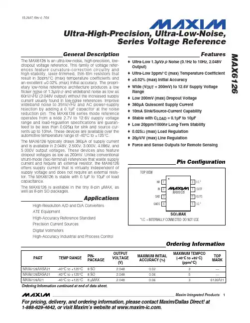
General DescriptionThe MAX6126 is an ultra-low-noise, high-precision, low-dropout voltage reference. This family of voltage refer-ences feature curvature-correction circuitry and high-stability, laser-trimmed, thin-film resistors that result in 3ppm/°C (max) temperature coefficients and an excellent ±0.02% (max) initial accuracy. The propri-etary low-noise reference architecture produces a low flicker noise of 1.3µV P-P and wideband noise as low as 60nV/√Hz (2.048V output) without the increased supply current usually found in low-noise references. Improve wideband noise to 35nV/√Hz and AC power-supply rejection by adding a 0.1µF capacitor at the noise reduction pin. The MAX6126 series mode reference operates from a wide 2.7V to 12.6V supply voltage range and load-regulation specifications are guaran-teed to be less than 0.025Ωfor sink and source cur-rents up to 10mA. These devices are available over the automotive temperature range of -40°C to +125°C.The MAX6126 typically draws 380µA of supply current and is available in 2.048V, 2.500V, 3.000V, 4.096V, and 5.000V output voltages. These devices also feature dropout voltages as low as 200mV. Unlike conventional shunt-mode (two-terminal) references that waste supply current and require an external resistor, the MAX6126offers supply current that is virtually independent of supply voltage and does not require an external resis-tor. The MAX6126 is stable with 0.1µF to 10µF of load capacitance.The MAX6126 is available in the tiny 8-pin µMAX, as well as 8-pin SO packages.ApplicationsHigh-Resolution A/D and D/A Converters ATE EquipmentHigh-Accuracy Reference Standard Precision Current Sources Digital VoltmetersHigh-Accuracy Industrial and Process ControlFeatures♦Ultra-Low 1.3µV P-P Noise (0.1Hz to 10Hz, 2.048V Output)♦Ultra-Low 3ppm/°C (max) Temperature Coefficient ♦±0.02% (max) Initial Accuracy♦Wide (V OUT + 200mV) to 12.6V Supply Voltage Range ♦Low 200mV (max) Dropout Voltage ♦380µA Quiescent Supply Current ♦10mA Sink/Source-Current Capability ♦Stable with C LOAD = 0.1µF to 10µF ♦Low 20ppm/1000hr Long-Term Stability ♦0.025Ω(max) Load Regulation ♦20µV/V (max) Line Regulation♦Force and Sense Outputs for Remote SensingMAX6126Ultra-High-Precision, Ultra-Low-Noise,Series Voltage Reference________________________________________________________________Maxim Integrated Products1Pin ConfigurationOrdering Information19-2647; Rev 4; 7/04For pricing, delivery, and ordering information,please contact Maxim/Dallas Direct!at 1-888-629-4642, or visit Maxim’s website at .Ordering Information continued at end of data sheet.M A X 6126Ultra-High-Precision, Ultra-Low-Noise, Series Voltage Reference 2_______________________________________________________________________________________ABSOLUTE MAXIMUM RATINGSStresses beyond those listed under “Absolute Maximum Ratings” may cause permanent damage to the device. These are stress ratings only, and functional operation of the device at these or any other conditions beyond those indicated in the operational sections of the specifications is not implied. Exposure to absolute maximum rating conditions for extended periods may affect device reliability.(All voltages referenced to GND)GNDS ....................................................................-0.3V to +0.3V IN...........................................................................-0.3V to +13V OUTF, OUTS, NR........-0.3V to the lesser of (V IN + 0.3V) or +6V Output Short Circuit to GND or IN..........................................60s Continuous Power Dissipation (T A = +70°C)8-Pin µMAX (derate 4.5mW/°C above +70°C) ............362mW 8-Pin SO (derate 5.88mW/°C above +70°C) ...............471mWOperating Temperature Range ........................-40°C to +125°C Junction Temperature .....................................................+150°C Storage Temperature Range ............................-65°C to +150°C Lead Temperature (soldering, 10s) ................................+300°CELECTRICAL CHARACTERISTICS—MAX6126_21 (V OUT = 2.048V)MAX6126Ultra-High-Precision, Ultra-Low-Noise,Series Voltage Reference_______________________________________________________________________________________3ELECTRICAL CHARACTERISTICS—MAX6126_21 (V OUT = 2.048V) (continued)ELECTRICAL CHARACTERISTICS—MAX6126_25 (V OUT = 2.500V)M A X 6126Ultra-High-Precision, Ultra-Low-Noise, Series Voltage ReferenceELECTRICAL CHARACTERISTICS—MAX6126_25 (V OUT = 2.500V) (continued)(V IN = 5V, C LOAD = 0.1µF, I OUT = 0, T A = T MIN to T MAX , unless otherwise noted. Typical values are at T A = +25°C.)ELECTRICAL CHARACTERISTICS—MAX6126_30 (V OUT = 3.000V)(V IN = 5V, C LOAD = 0.1µF, I OUT = 0, T A = T MIN to T MAX , unless otherwise noted. Typical values are at T A = +25°C.)MAX6126Ultra-High-Precision, Ultra-Low-Noise,Series Voltage Reference_______________________________________________________________________________________5ELECTRICAL CHARACTERISTICS—MAX6126_30 (V OUT = 3.000V) (continued)(V IN = 5V, C LOAD = 0.1µF, I OUT = 0, T A = T MIN to T MAX , unless otherwise noted. Typical values are at T A = +25°C.)ELECTRICAL CHARACTERISTICS—MAX6126_41 (V OUT = 4.096V)(V = 5V, C = 0.1µF, I = 0, T = T to T , unless otherwise noted. Typical values are at T = +25°C.)M A X 6126Ultra-High-Precision, Ultra-Low-Noise, Series Voltage Reference 6_______________________________________________________________________________________ELECTRICAL CHARACTERISTICS—MAX6126_41 (V OUT = 4.096V) (continued)(V= 5V, C = 0.1µF, I = 0, T = T to T , unless otherwise noted. Typical values are at T = +25°C.)MAX6126Ultra-High-Precision, Ultra-Low-Noise,Series Voltage Reference_______________________________________________________________________________________7ELECTRICAL CHARACTERISTICS—MAX6126_50 (V OUT = 5.000V)(V IN = 5.5V, C LOAD = 0.1µF, I OUT = 0, T A = T MIN to T MAX , unless otherwise noted. Typical values are at T A = +25°C.)M A X 6126Ultra-High-Precision, Ultra-Low-Noise, Series Voltage Reference 8_______________________________________________________________________________________ELECTRICAL CHARACTERISTICS—MAX6126_50 (V OUT = 5.000V) (continued)(V IN = 5.5V, C LOAD = 0.1µF, I OUT = 0, T A = T MIN to T MAX , unless otherwise noted. Typical values are at T A = +25°C.)Note 2:Thermal hysteresis is defined as the change in +25°C output voltage before and after cycling the device from T MAX to T MIN .Note 3:Dropout voltage is defined as the minimum differential voltage (V IN - V OUT ) at which V OUT decreases by 0.1% from itsoriginal value at V IN = 5.0V (V IN = 5.5V for V OUT = 5.0V).Typical Operating Characteristics(V IN = 5V for MAX6126_21/25/30/41, V IN = 5.5V for MAX6126_50, C LOAD = 0.1µF, I OUT = 0, T A = +25°C, unless otherwise specified.)(Note 5)MAX6126A_21OUTPUT VOLTAGE TEMPERATURE DRIFT(V OUT = 2.048V) (SO)TEMPERATURE (°C)O U T P U T V O L T A G E (V )100755025-252.04652.04702.04752.04802.04852.04902.0460-50125MAX6126A_21OUTPUT VOLTAGE TEMPERATURE DRIFT(V OUT = 2.048V) (µMAX)TEMPERATURE (°C)O U T P U T V O L T A G E (V )100755025-252.04802.04752.04852.04902.0470-50125MAX6126A_50OUTPUT VOLTAGE TEMPERATURE DRIFT(V OUT = 5.000V) (SO)TEMPERATURE (°C)O U T P U T V O L T A G E (V )100755025-255.0004.9995.0015.0024.998-50125Typical Operating Characteristics (continued)(V IN = 5V for MAX6126_21/25/30/41, V IN = 5.5V for MAX6126_50, C LOAD = 0.1µF, I OUT = 0, T A = +25°C, unless otherwise specified.)(Note 5)MAX6126Ultra-High-Precision, Ultra-Low-Noise,Series Voltage Reference_______________________________________________________________________________________9MAX6126A_50OUTPUT VOLTAGE TEMPERATURE DRIFT(V OUT = 5.000V) (µMAX)TEMPERATURE (°C)O U T P U T V O L T A G E (V )100755025-255.0004.9995.0015.0024.998-50125MAX6126_21LOAD REGULATIONOUTPUT CURRENT (mA)O U T PU T V O L T A G E (V )5-52.04652.04702.04752.04802.04852.0460-1010MAX6126_50LOAD REGULATIONOUTPUT CURRENT (mA)O U T P U T V O L T A G E (V)5-54.9974.9984.9995.0005.0014.996-1010MAX6126_50POWER-SUPPLY REJECTION RATIOvs. FREQUENCYM A X 6126 t o c 10FREQUENCY (kHz)P S R R (d B )1001010.10.01-100-80-60-40-200-1200.0011000MAX6126_21SUPPLY CURRENT vs. INPUT VOLTAGEINPUT VOLTAGE (V)S U P P L Y C U R R E N T (µA )121086421002003004005006000014MAX6126_50SUPPLY CURRENT vs. INPUT VOLTAGEINPUT VOLTAGE (V)S U P P L Y C U R R E N T (µA )121068421002003004005006007008009000014MAX6126_25DROPOUT VOLTAGE vs. SOURCE CURRENTSOURCE CURRENT (mA)D R O P O U T V O L T A GE (m V )12963501001502002503000015MAX6126_50DROPOUT VOLTAGE vs. SOURCE CURRENTSOURCE CURRENT (mA)D R O P O U T V O L T A GE (m V )1296350100150200250015MAX6126_21POWER-SUPPLY REJECTION RATIOvs. FREQUENCYM A X 6126 t o c 09FREQUENCY (kHz)P S R R (d B )1001010.10.01-100-80-60-40-200-1200.0011000Typical Operating Characteristics (continued)(V IN = 5V for MAX6126_21/25/30/41, V IN = 5.5V for MAX6126_50, C LOAD = 0.1µF, I OUT = 0, T A = +25°C, unless otherwise specified.)(Note 5)M A X 6126Ultra-High-Precision, Ultra-Low-Noise, Series Voltage Reference 10______________________________________________________________________________________MAX6126_21OUTPUT NOISE (0.1Hz TO 10Hz)1s/div 0.4µV/div V OUT = 2.048VMAX6126_50OUTPUT NOISE (0.1Hz TO 10Hz)1s/div1µV/divV OUT = 5VMAX6126_21LOAD TRANSIENTMAX6126 toc15200µs/div0mA10mA V OUTAC-COUPLED 100mV/divC LOAD = 0.1µF V IN = 5VI OUT 5mA/div I OUT = 0 TO 10mA V OUT = 2.048VMAX6126_21LOAD TRANSIENTMAX6126 toc16200µs/div C LOAD = 0.1µF V IN = 5VI OUT = -100µA TO 1mA V OUT = 2.048V-100µA1mA VOUTAC-COUPLED 20mV/divI OUT500µA/div MAX6126_21LOAD TRANSIENTMAX6126 toc17400µs/divC LOAD = 0.1µF V IN = 5VI OUT = -1mA TO -10mA V OUT = 2.048V-10mA-1mA V OUTAC-COUPLED 100mV/divI OUT 5mA/div MAX6126_21LOAD TRANSIENTMAX6126 toc181ms/div C LOAD = 10µF V IN = 5VI OUT = 0 TO 10mA V OUT = 2.048V0mA 10mA V OUTAC-COUPLED 20mV/divI OUT 5mA/divTypical Operating Characteristics (continued)(V IN = 5V for MAX6126_21/25/30/41, V IN = 5.5V for MAX6126_50, C LOAD = 0.1µF, I OUT = 0, T A = +25°C, unless otherwise specified.)(Note 5)MAX6126Series Voltage Reference______________________________________________________________________________________11MAX6126_21LOAD TRANSIENTMAX6126 toc191ms/divC LOAD = 10µF V IN = 5VI OUT = -100µA TO 1mA V OUT = 2.048V-100µA+1mA V OUTAC-COUPLED 10mV/div I OUT500µA/div MAX6126_21LOAD TRANSIENTMAX6126 toc20400µs/div C LOAD = 10µF V IN = 5VI OUT = -1mA TO -10mA V OUT = 2.048V-10mA-1mA V OUTAC-COUPLED 50mV/divI OUT5mA/div MAX6126_21LINE TRANSIENTMAX6126 toc212.7V3.2V V OUTAC-COUPLED 20mV/div V IN200mV/div 20µs/divV OUT = 2.048VC LOAD = 0.1µFMAX6126_50LINE TRANSIENTMAX6126 toc225.2V5.7V V OUTAC-COUPLED 10mV/divV IN200mV/div 400µs/div V IN = 5.2V TO 5.7V V OUT = 5VC LOAD = 0.1µFMAX6126_21TURN-ON TRANSIENTMAX6126 toc2320µs/divGND 5.5V V OUT 1V/divV IN 2V/div C LOAD = 0.1µF V OUT = 2.048VMAX6126_50TURN-ON TRANSIENTMAX6126 toc24GND 5.5V V OUT 2V/div V IN 2V/div GND200µs/divC LOAD = 0.1µF V OUT = 5VTypical Operating Characteristics (continued)(V IN = 5V for MAX6126_21/25/30/41, V IN = 5.5V for MAX6126_50, C LOAD = 0.1µF, I OUT = 0, T A = +25°C, unless otherwise specified.)(Note 5)M A X 6126Series Voltage Reference 12______________________________________________________________________________________MAX6126_21TURN-ON TRANSIENTMAX6126 toc25GND5.5V V OUT 1V/divV IN 2V/div 40µs/divC LOAD = 10µF V OUT= 2.048VMAX6126_50TURN-ON TRANSIENTMAX6126 toc26GND 5.5V V OUT 2V/div V IN 2V/divGND400µs/div C LOAD = 10µF V OUT = 5V2.49942.49982.49962.50022.50002.50042.500604002006008001000MAX6126B_25LONG-TERM STABILITY vs. TIME (SO)TIME (hr)V O U T (V )2.50102.50052.50002.49952.499004002006008001000MAX6126B_25LONG-TERM STABILITY vs. TIME (µMAX)TIME (hr)V O U T (V )4.99944.99984.99965.00025.00005.00045.000604002006008001000MAX6126B_50LONG-TERM STABILITY vs. TIME (SO)TIME (hr)V O U T (V )5.00105.00055.00004.99954.99904002006008001000MAX6126B_50LONG-TERM STABILITY vs. TIME (µMAX)TIME (hr)V O U T (V )Note 5:Many of the MAX6126 Typical Operating Characteristics are extremely similar. The extremes of these characteristics arefound in the MAX6126_21 (2.048V output) and the MAX6126_50 (5.000V output). The Typical Operating Characteristics of the remainder of the MAX6126 family typically lie between those two extremes and can be estimated based on their output voltages.MAX6126Series Voltage Reference______________________________________________________________________________________13Detailed DescriptionWideband Noise ReductionTo improve wideband noise and transient power-supply noise, add a 0.1µF capacitor to NR (Figure 1). Larger values do not improve noise appreciably. A 0.1µF NR capacitor reduces the noise from 60nV/√Hz to 35nV/√Hz for the 2.048V output. Noise in the power-supply input can affect output noise, but can be reduced by adding an optional bypass capacitor between IN and GND, as shown in the Typical Operating Circuit .Output BypassingThe MAX6126 requires an output capacitor between 0.1µF and 10µF. Locate the output capacitor as close to OUTF as possible. For applications driving switching capacitive loads or rapidly changing load currents, it is advantageous to use a 10µF capacitor in parallel with a 0.1µF capacitor. Larger capacitor values reduce tran-sients on the reference output.Supply CurrentThe quiescent supply current of the series-mode MAX6126 family is typically 380µA and is virtually inde-pendent of the supply voltage, with only a 2µA/V (max)variation with supply voltage.When the supply voltage is below the minimum speci-fied input voltage during turn-on, the device can drawup to 300µA beyond the nominal supply current. The input voltage source must be capable of providing this current to ensure reliable turn-on.Thermal HysteresisThermal hysteresis is the change of output voltage at T A = +25°C before and after the device is cycled over its entire operating temperature range. The typical ther-mal hysteresis value is 20ppm (SO package).Turn-On TimeThese devices typically turn on and settle to within 0.1% of their final value in 200µs to 2ms depending on the device. The turn-on time can increase up to 4ms with the device operating at the minimum dropout volt-age and the maximum load. A noise reduction capaci-tor of 0.1µF increases the turn-on time to 20ms.Output Force and SenseThe MAX6126 provides independent connections for the power-circuit output (OUTF) supplying current into a load, and for the circuit input regulating the voltage applied to that load (OUTS). This configuration allows for the cancellation of the voltage drop on the lines connect-ing the MAX6126 and the load. When using the Kelvin connection made possible by the independent current and voltage connections, take the power connection to the load from OUTF, and bring a line from OUTS to join the line from OUTF, at the point where the voltage accu-M A X 6126Series Voltage Reference 14______________________________________________________________________________________racy is needed. The MAX6126 has the same type of Kelvin connection to cancel drops in the ground return line. Connect the load to ground and bring a connection from GNDS to exactly the same point.Applications InformationPrecision Current SourceFigure 2 shows a typical circuit providing a precision current source. The OUTF output provides the bias cur-rent for the bipolar transistor. OUTS and GNDS sense the voltage across the resistor and adjust the current sourced by OUTF accordingly. For even higher preci-sion, use a MOSFET to eliminate base current errors.High-Resolution DAC and Reference froma Single SupplyFigure 3 shows a typical circuit providing the reference for a high-resolution, 16-bit MAX541 D/A converter.Temperature Coefficient vs. Operating Temperature Range for a 1 LSB MaximumErrorIn a data converter application, the reference voltage of the converter must stay within a certain limit to keep the error in the data converter smaller than the resolution limit through the operating temperature range. Figure 4shows the maximum allowable reference voltage tem-perature coefficient to keep the conversion error to less than 1 LSB, as a function of the operating temperature range (T MAX - T MIN ) with the converter resolution as a parameter. The graph assumes the reference voltage temperature coefficient as the only parameter affecting accuracy.In reality, the absolute static accuracy of a data con-verter is dependent on the combination of many para-meters such as integral nonlinearity, differential nonlinearity, offset error, gain error, as well as voltage reference changes.Figure 2. Precision Current SourceMAX6126Series Voltage Reference______________________________________________________________________________________15Figure 4. Temperature Coefficient vs. Operating Temperature Range for a 1 LSB Maximum ErrorChip InformationTRANSISTOR COUNT: 1171PROCESS: BiCMOSTypical Operating CircuitM A X 6126Series Voltage Reference 16______________________________________________________________________________________Ordering Information (continued)MAX6126Series Voltage Reference______________________________________________________________________________________17Package Information(The package drawing(s) in this data sheet may not reflect the most current specifications. For the latest package outline information,go to /packages .M A X 6126Series Voltage Reference Maxim cannot assume responsib ility for use of any circuitry other than circuitry entirely emb odied in a Maxim product. No circuit patent licenses are implied. Maxim reserves the right to change the circuitry and specifications without notice at any time.18____________________Maxim Integrated Products, 120 San Gabriel Drive, Sunnyvale, CA 94086 408-737-7600©2004 Maxim Integrated ProductsPrinted USAis a registered trademark of Maxim Integrated Products.Package Information (continued)(The package drawing(s) in this data sheet may not reflect the most current specifications. For the latest package outline information,go to /packages .。