电子元器件ZXCT1050中文资料_数据手册_IC数据表
- 格式:pdf
- 大小:558.38 KB
- 文档页数:9
ZXCT1010Enhanced high-side current monitorDescriptionOrdering informationThe ZXCT1010 is a high side current sense monitor. Using this device eliminates the need to disrupt the ground plane when sensing a load current.t is an enhanced version of the ZXCT1009offering reduced typical output offset and improved accuracy at low sense voltage.The wide input voltage range of 20V down to as low as 2.5V make it suitable for a range of applications. A minimum operating current of just 4A, combined with its SOT23-5 package make suitable for portable battery equipment.Features•Low cost, accurate high-side current sensing•Output voltage scaling •Up to 2.5V sense voltage • 2.5V – 20V supply range •300nA typical offset current • 3.5A quiescent current •1% typical accuracy •SOT23-5 packageApplications•Battery chargers •Smart battery packs •DC motor control •Over current monitor •Power management•Programmable current sourcePinout informationTypical application circuitDevicePackage Device marking Reel size (inches)Tape width (mm)Quantity per reel ZXCT1010E5TASOT23-5101783000https:///Pin informationAbsolute maximum ratingsOperation above the absolute maximum rating may cause device failure. Operation at the absolute maximum ratings, for extended periods, may reduce device reliability.Pin Name Description 1N/C Not connection2GND Ground connection3I OUTOutput current, proportional to V IN - V LOAD4V SENSE+Supply voltage5V SENSE-Connection to load/batteryVoltage on any pin (relative to GND pin)-0.6 to 20V (relative to GND)Continuous output current 25mAContinous sense voltageV IN + 0.5V > V SENSE > V IN - 5V Ambient operating temperature range -40 to 85°C Storage temperature -55 to 150°C Package power dissipation T amb = 25°C SOT23-5300mWhttps:///Electrical characteristicsTest conditions T amb = 25°C, V IN = 5V, R OUT = 100⍀NOTES:(a)Includes input offset voltage contribution (b)V SENSE = V IN -V LOAD(c)-20dBm = 63mVp-p into 50⍀Symbol ParameterConditionsLimits UnitMin.Typ.Max.V IN V CC range 2.520V I OUT (a)Output currentV SENSE = 0V 00.310A V SENSE = 10mV 85100115A V SENSE = 100mV 0.975 1.00 1.025mAV SENSE = 200mV 1.95 2.00 2.05mA V SENSE = 1V9.710.010.3mA I Q Ground pin current V SENSE = 0V3.58A V SENSE (b)Sense voltage2500mV I SENSE-V SENSE- input current 100nAAcc AccuracyR SENSE = 0.1⍀ V SENSE = 200mV-2.52.5%Gm Transconductance, I OUT /V SENSE 10000A/VBWBandwidthRF P IN = -20dBm (c)V SENSE = 10mV DC 300kHz VSENSE= 100mV DC 2MHzhttps:///Typical characteristicsPower dissipationThe maximum allowable power dissipation of the device Array for normal operation (P max), is a function of the packagejunction to ambient thermal resistance (⍜ja), maximumjunction temperature (Tj max), and ambient temperature(T amb), according to the expression:Pmax = (Tj max – T amb) / ⍜jaThe device power dissipation, P D is given by theexpression:P D=I OUT.(V IN-V OUT) WattsApplications informationThe following lines describe how to scale a load current to an output voltage.V SENSE = V IN - V LOADV OUT = 0.01 x V SENSE x R OUT(1)For example:https:/// A 1A current is to be represented by a 100mV output voltage:1Choose the value of R SENSE to give 50mV > V SENSE > 500mV at full load.For example V SENSE = 100mV at 1.0A. R SENSE = 0.1/1.0 => 0.1⍀.2Choose R OUT to give V OUT = 100mV, when V SENSE = 100mV.Rearranging (1)for R OUT gives:R OUT = V OUT /(V SENSE x 0.01)R OUT = 0.1 / (0.1 x 0.01) = 100⍀Schematic diagramTypical circuit applicationWhere R LOAD represents any load including DC Array motors, a charging battery or further circuitrythat requires monitoring, R SENSE can beselected on specific requirements of accuracy,size and power rating.Li-Ion charger circuitThe figure below shows the ZXCT1010 supporting the Benchmarq bq2954 charge managementIC. Most of the support components for the bq2954 are omitted for clarity. This design also usesthe Zetex FZT789A high current Super- PNP as the switching transistor in the DC-DC step downconverter and the FMMT451 as the drive NPN for the FZT789A. The circuit can be configured to https:///charge up to four Li-Ion cells at a charge current of 1.25A. Charge can be terminated on maximumvoltage, selectable minimum current, or maximum time out. Switching frequency of the PWMloop is approximately 120kHz.Bi-directional current sensingThe ZXCT1010 can be used to measure current bi-Array directionally, if two devices are connected as shownopposite.If the voltage V1 is positive with respect to the voltage V2the lower device will be active, delivering a proportionaloutput current to R OUT. Due to the polarity of the voltageacross Rsense, the upper device will be inactive and will notcontribute to the current delivered to R OUT. When V2 is morepositive than V1, current will be flowing in the oppositedirection, causing the upper device to be active instead.Non-linearity will be apparent at small values of V SENSE dueto offset current contribution. Devices can use separateoutput resistors if the current direction is to be monitoredindependently.https:///Bi-directional transfer functionPCB trace shunt resistor for low cost solution The figure opposite shows output characteristics of the device when using a PCB resistive trace for a low cost solution in replacement for a conventional shunt resistor. The graph shows the linear rise in voltage across the resistor due to the PTC of the material and demonstrates how this rise in resistance value over temperature compensates for the NTC of the device. The figure below shows a PCB layout suggestion.The resistor section is 25mm x 0.25mm giving approximately 150mW using 1oz copper. The data for the normalised graph was obtained using a 1A load current and a 100W output resistor. An electronic version of the PCB layout is available at /isenseLayout shows area of shunt resistor compared to ZSOT23-5package (not actual size).https:///https:///Intentionally left blankPackage outline - SOT23-5Note: Controlling dimensions are in millimeters. Approximate dimensions are provided in inchesDIM MillimetersInchesMin.Max.Min.Max.A 0.90 1.450.03540.0570A10.000.150.000.0059A20.90 1.300.03540.0511b 0.200.500.00780.0196C 0.090.260.00350.0102D 2.70 3.100.10620.1220E 2.20 3.200.08660.1181E1 1.301.800.05110.0708e 0.95 REF 0.0374 REF e1 1.90 REF0.0748 REFL 0.100.600.00390.0236a°0°30°0°30°https:///。
ZXCT1080High voltage high-side current monitorDescriptionOrdering informationThe ZXCT1080 is a high side current sense monitor with a gain of 10 and a voltage output. Using this device eliminates the need to disrupt the ground plane when sensing a load current.The wide input voltage range of 60V down to as low as 3V make it suitable for a range of applications; including systems operating from industrial 24-28V rails and -48V rails.The separate supply pin (V CC ) allows the device to continue functioning under short circuit conditions, giving an end stop voltage at the output.The ZXCT1080 has an extended ambient operating temperature range of -40°C to 125°C enabling it to be used in a wide range of applications including automotive.Features•3V to 60V continuous high side voltage •Accurate high-side current sensing •-40 to 125°C temperature range •Output voltage scaling x10• 4.5V to 12V V CC range •Low quiescent current:•70µA supply pin •50µA I SENSE+•SOT23-5 package Applications•Industrial applications current measurement •Battery management •Over current monitor •Power management•Automotive current measurementPin connectionsTypical application circuitDevicePackage Part mark Reel size (inches)Tape width (mm)Quantity perreelZXCT1080E5TASOT23-51080783000https://Absolute maximum ratingsContinuous voltage on S- and S+-0.6 and 65V Voltage on all other pins-0.6V and +14VDifferential sense voltage, V SENSE 800mV Operating temperature -40 to 125°C Storage temperature-55 to 150°C Maximum junction temperature 125°CPackage power dissipation300mW * at T A = 25°COperation above the absolute maximum rating may cause device failure. Operation at the absolute maximum ratings, for extended periods, may reduce device reliability.V SENSE is defined as the differential voltage between S+ and S- pins.*Assumes ⍜JA = 420°C/WRecommended operating conditionsPin function tableParameterMin.Max.Units V IN Common-mode sense+ input range 360V V CCSupply voltage range4.512V V SENSE Differential sense input voltage range 00.15V V OUT Output voltage range 0 1.5V T AAmbient temperature range-40125°CPin Name Description1V CC This is the analogue supply and provides power to internal circuitry 2GND Ground pin3OUT Output voltage pin. NMOS source follower with 20µA bias to ground 4S+This is the positive input of the current monitor and has an input range from 60V down to 3V. The current through this pin varies with differential sense voltage5S-This is the negative input of the current monitor and has an input range from 60V down to 3Vhttps://Electrical characteristicsTest conditions T A = 25°C, V IN = 12V, V CC = 5 V, V SENSE (a) = 100mV unless otherwise stated.NOTES:(a)V SENSE = "V SENSE+" - "V SENSE-"(b)The ZXCT1080 operates from a positive power rail and the internal voltage-current converter current flow is unidirectional; these result in the output offset voltage for V SENSE = 0V always being positive.(c)For V SENSE > 10mV, the internal voltage-current converter is fully linear. This enables a true offset to be defined and used. V O(10) is expressed as the variance about an output voltage of 100mV>(d)Temperature dependent measurements are extracted from characterization and simulation results.(e)All Min and Max specifications over full temperature range are guaranteed by design and characterisationSymbol ParameterConditions T A Min (e).Typ.Max (e).Units I CC V CC supply current V CC = 12V, V SENSE (a) = 0V 25°C 4080120µAfull range 145I S+S+ input current V SENSE (a) = 0V25°C 152742µA full range 60I S-S- input current25°C 154080nA V O(0)Zero V SENSE (a) error (b)25°C 035mV V O(10)Output offset voltage (c)V SENSE (a) = 10mV 25°C -25+25mV full range -55+55Gain⌬V OUT /⌬V SENSE (a)V SENSE (a) = 10mV to150mV 25°C 9.91010.1V/V full range9.810.2V OUT TC (d)V OUT variation withtemperature 30ppm/°C Acc Total output error -33%I OH Output source current⌬V OUT = -30mV 1mA I OL Output sink current⌬V OUT = +30mV20µA PSRR V CC supply rejection ratioV CC = 4.5V to 12V 5460dB CMRR Common-mode sense rejection ratio V IN = 60V to 3V 6880dB BW-3dB small signal bandwidthV SENSE (a) (AC) = 10mV PP500kHz https://Typical characteristicsTest conditions unless otherwise stated: T A = 25°C, V CC = 5V, V SENSE+ =12V, V SENSE = 100mVTypical characteristicsTest conditions unless otherwise stated: T A = 25°C, V CC = 5V, V SENSE+ =12V, V SENSE = 100mVTypical characteristicsTest conditions unless otherwise stated: T A = 25°C, V CC = 5V, V SENSE+ =12V, V SENSE = 100mVhttps://Application informationThe ZXCT1080 has been designed to allow it to operate with 5V supply rails while sensing common mode signals up to 60V. This makes it well suited to a wide range of industrial and power supply monitoring applications that require the interface to 5V systems while sensing much higher voltages.To allow this its V CC pin can be used independently of S+.Figure 1 shows the basic configuration of the ZXCT1080.Figure 1Typical configuration of ZXCT1080Load current from the input is drawn through R SENSE developing a voltage V SENSE across the inputs of the ZXCT1080.The internal amplifier forces V SENSE across internal resistance R GT causing a current to flow through MOSFET M1. This current is then converted to a voltage by R G . A ratio of 10:1 between R G and R GT creates the fixed gain of 10. The output is then buffered by the unity gain buffer.The gain equation of the ZXCT1080 is:The maximum recommended differential input voltage, V SENSE , is 150mV; it will howeverwithstand voltages up to 800m ⍀. This can be increased further by the inclusion of a resistor, R LIM ,between S- pin and the load; typical value is of the order of 10k .V OUT I L R SENSE R GRGT---------1×I L R SENSE ×10×==https://Figure 2Protection/error sources for ZXCT1080Capacitor C D provides high frequency transient decoupling when used with R LIM ; typical values are of the order 10pFFor best performance R SENSE should be connected as close to the S+ (and SE NSE ) pins;minimizing any series resistance with R SENSE .When choosing appropriate values for R SENSE a compromise must be reached between in-line signal loss (including potential power dissipation effects) and small signal accuracy.Higher values for R SENSE gives better accuracy at low load currents by reducing the inaccuracies due to internal offsets. For best operation the ZXCT1080 has been designed to operate with V SENSE of the order of 50mV to 150mV.Current monitors' basic configuration is that of a unipolar voltage to current to voltage converter powered from a single supply rail. The internal amplifier at the heart of the current monitor may well have a bipolar offset voltage but the output cannot go negative; this results in current monitors saturating at very low sense voltages.As a result of this phenomenon the ZXCT1080 has been specified to operate in a linear manner over a V SENSE range of 10mV to 150mV range, however it will still be monotonic down to VSENSE of 0V.It is for this very reason that Zetex has specified an input offset voltage (V O(10)) at 10mV. The output voltage for any V SENSE voltage from 10mV to 150mV can be calculated as follows:Alternatively the load current can be expressed as:V OUT V SENSE ()xG V O 10()+=I L V OUT V O 10()–()GxR SENSE------------------------------------------=https://Package details - SOT23-5Note: Controlling dimensions are in millimeters. Approximate dimensions are provided in inchesDIM MillimetersInchesMin.Max.Min.Max.A - 1.00-0.0393A10.010.100.00030.0039A20.840.900.03300.0354b 0.300.450.01180.0177c 0.120.200.00470.0078D 2.90 BSC 0.114 BSCE 2.80 BSC 0.110 BSC E1 1.60 BSC 0.062 BSC e 0.95 BSC 0.0374 BSC e1 1.90 BSC0.0748 BSCL 0.300.500.01180.0196L20.25 BSC 0.010 BSC a°4°12°4°12°https://ZXCT1080DefinitionsProduct changeZetex Semiconductors reserves the right to alter, without notice, specifications, design, price or conditions of supply of any product or service. Customers are solely responsible for obtaining the latest relevant information before placing orders.Applications disclaimerThe circuits in this design/application note are offered as design ideas. It is the responsibility of the user to ensure that the circuit is fit for the user’s application and meets with the user’s requirements. No representation or warranty is given and no liability whatsoever is assumed by Zetex with respect to the accuracy or use of such information, or infringement of patents or other intellectual property rights arising from such use or otherwise. Zetex does not assume any legal responsibility or will not be held legally liable (whether in contract,tort (including negligence), breach of statutory duty, restriction or otherwise) for any damages, loss of profit, business, contract,opportunity or consequential loss in the use of these circuit applications, under any circumstances.Life supportZetex products are specifically not authorized for use as critical components in life support devices or systems without the express written approval of the Chief Executive Officer of Zetex Semiconductors plc. As used herein:A. Life support devices or systems are devices or systems which:1.are intended to implant into the bodyor 2.support or sustain life and whose failure to perform when properly used in accordance with instructions for use provided in thelabelling can be reasonably expected to result in significant injury to the user.B. A critical component is any component in a life support device or system whose failure to perform can be reasonably expected tocause the failure of the life support device or to affect its safety or effectiveness.ReproductionThe product specifications contained in this publication are issued to provide outline information only which (unless agreed by the company in writing) may not be used, applied or reproduced for any purpose or form part of any order or contract or be regarded as a representation relating to the products or services concerned.Terms and ConditionsAll products are sold subjects to Zetex’ terms and conditions of sale, and this disclaimer (save in the event of a conflict between the two when the terms of the contract shall prevail) according to region, supplied at the time of order acknowledgement.For the latest information on technology, delivery terms and conditions and prices, please contact your nearest Zetex sales office.Quality of productZetex is an ISO 9001 and TS16949 certified semiconductor manufacturer.To ensure quality of service and products we strongly advise the purchase of parts directly from Zetex Semiconductors or one of our regionally authorized distributors. For a complete listing of authorized distributors please visit: /salesnetworkZetex Semiconductors does not warrant or accept any liability whatsoever in respect of any parts purchased through unauthorized sales channels.ESD (Electrostatic discharge)Semiconductor devices are susceptible to damage by ESD. Suitable precautions should be taken when handling and transporting devices.The possible damage to devices depends on the circumstances of the handling and transporting, and the nature of the device. The extent of damage can vary from immediate functional or parametric malfunction to degradation of function or performance in use over time.Devices suspected of being affected should be replaced.Green complianceZetex Semiconductors is committed to environmental excellence in all aspects of its operations which includes meeting or exceeding regulatory requirements with respect to the use of hazardous substances. Numerous successful programs have been implemented to reduce the use of hazardous substances and/or emissions.All Zetex components are compliant with the RoHS directive, and through this it is supporting its customers in their compliance with WEEE and ELV directives.Product status key:“Preview”Future device intended for production at some point. Samples may be available“Active”Product status recommended for new designs“Last time buy (LTB)”Device will be discontinued and last time buy period and delivery is in effect“Not recommended for new designs”Device is still in production to support existing designs and production“Obsolete”Production has been discontinuedDatasheet status key:“Draft version”This term denotes a very early datasheet version and contains highly provisional information, which may change in any manner without notice.“Provisional version”This term denotes a pre-release datasheet. It provides a clear indication of anticipated performance.However, changes to the test conditions and specifications may occur, at any time and without notice.“Issue”This term denotes an issued datasheet containing finalized specifications. However, changes tospecifications may occur, at any time and without notice.https://。
CTM1050广州致远电子有限公司 工业通讯网络事业部———————————————概述CTM1050是一款带隔离的高速CAN 收发器芯片,该芯片内部集成了所有必需的CAN 隔离及CAN 收、发器件,这些都被集成在不到3平方厘米的芯片上。
芯片的主要功能是将CAN 控制器的逻辑电平转换为CAN 总线的差分电平并且具有DC 2500V 的隔离功能及ESD 保护作用。
和TJA1050一样,该芯片符合ISO 11898标准,因此,它可以和其他遵从ISO 11898标准的CAN 收发器产品互操作。
——————————————产品特性 具有隔离、ESD 保护功能;完全符合ISO11898标准的CAN 收发器; 通讯速率最高达1Mbps; 隔离电压:DC 2500V; 电磁辐射EME 极低; 电磁抗干扰EMI 性极高; 无需外加元件可直接使用; 至少可连接110个节点;高低温特性好,能满足工业级产品技术要求。
注:CTM1050T 除具有以上特性外,还具有TVS 管 防总线过压。
————————————产品应用 ◆ 汽车电子 ◆ 仪器、仪表 ◆ 石油化工 ◆ 电力监控 ◆ ……—————————————订购信息型号温度范围 封装CTM1050 -40℃—+85℃ DIP-8Pin CTM1050T-40℃—+85℃DIP-8Pin————————————————————————————————典型应用图 1 CTM1050应用示例如图1所示为CTM1050的应用示例,该芯片可以连接任何一款CAN 协议控制器,实现CAN 节点的收发与隔离功能。
在以往的设计方案中需要光耦、DC/DC 隔离、CAN 收发器等其他元器件才能实现带隔离的CAN 收发电路,但现在您只需利用一片CTM1050接口芯片就可以实现带隔离的CAN 收发电路,隔离电压可以达到DC 2500V ,其接口简单,使用方便,是嵌入式系统的理想选择!共享修订历史版本日期原因Rev X1 2006/6/8 内部制定初稿Rev 1.0 2006/6/16 第一次发布Rev 1.1 2006/11/11 数据手册升级共享目录销售信息 (2)技术支持 (2)1. 功能简介 (3)2. 引脚信息 (4)2.1 CTM1050引脚信息 (4)3. CTM1050特性参数 (5)3.1 参数列表 (5)3.2 电气特性 (5)3.3 绝缘特性 (6)4. 机械尺寸 (7)4.1 CTM1050机械尺寸 (7)5. 电路连接 (8)5.1 CTM1050电路连接 (8)6. 声明 (9)共享销售信息如果需要购买本产品,请在办公时间(星期一至五上午8:30~11:50;下午1:30~5:30;星期六上午8:30~11:50)拨打电话咨询广州致远电子有限公司。
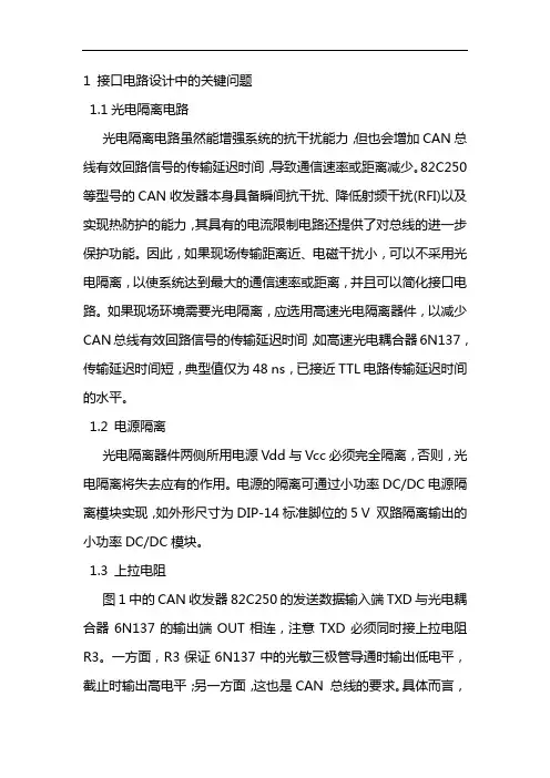
1 接口电路设计中的关键问题1.1光电隔离电路光电隔离电路虽然能增强系统的抗干扰能力,但也会增加CAN总线有效回路信号的传输延迟时间,导致通信速率或距离减少。
82C250等型号的CAN收发器本身具备瞬间抗干扰、降低射频干扰(RFI)以及实现热防护的能力,其具有的电流限制电路还提供了对总线的进一步保护功能。
因此,如果现场传输距离近、电磁干扰小,可以不采用光电隔离,以使系统达到最大的通信速率或距离,并且可以简化接口电路。
如果现场环境需要光电隔离,应选用高速光电隔离器件,以减少CAN总线有效回路信号的传输延迟时间,如高速光电耦合器6N137,传输延迟时间短,典型值仅为48 ns,已接近TTL电路传输延迟时间的水平。
1.2 电源隔离光电隔离器件两侧所用电源Vdd与Vcc必须完全隔离,否则,光电隔离将失去应有的作用。
电源的隔离可通过小功率DC/DC电源隔离模块实现,如外形尺寸为DIP-14标准脚位的5 V 双路隔离输出的小功率DC/DC模块。
1.3 上拉电阻图1中的CAN收发器82C250的发送数据输入端TXD与光电耦合器6N137的输出端OUT相连,注意TXD必须同时接上拉电阻R3。
一方面,R3保证6N137中的光敏三极管导通时输出低电平,截止时输出高电平;另一方面,这也是CAN 总线的要求。
具体而言,82C250的TXD端的状态决定着高、低电平CAN 电压输入/输出端CANH、CANL的状态(见表1)。
CAN总线规定,总线在空闲期间应呈隐性,即CAN 网络中节点的缺省状态是隐性,这要求82C25O 的TXD端的缺省状态为逻辑1(高电平)。
为此,必须通过R3确保在不发送数据或出现异常情况时,TXD端的状态为逻辑1(高电平)。
1.4总线阻抗匹配CAN总线的末端必须连接2个120Ω的电阻,它们对总线阻抗匹配有着重要的作用,不可省略。
否则,将大大降低总线数据通信时的可靠性和抗干扰性,甚至有可能导致无法通信。
1.5 其它抗干扰措施为提高接口电路的抗干扰能力,还可考虑以下措施:(1)在82C25O的CANH、CANL端与地之间并联2个30 pF的小电容,以滤除总线上的高频干扰,防止电磁辐射。
tja1050中文资料嵌入式架构有多重要?要做到嵌入式应用的代码逻辑清晰,且避免重复的造轮子,没有好的应用架构怎么行?如果没有好的架构,移植将会是一件很痛苦的事情。
如果没有好的架构,复用是最大的难题,没法更大限度的复用原有的代码。
如果没有好的架构,一旦驱动改了,所有的地方都要改,费时费力且很容易出错。
如果没有好的架构,应用层中穿插着硬件驱动层的代码,看着会是一片混乱,逻辑不清,代码维护起来会很困难。
接下来嵌入式ARM便和大家分享一下,嵌入式架构那些事儿……01嵌入式系统的基本架构嵌入式系统一般由软件和硬件两个部分组成,基中嵌入式处理器、存储器和外部设备构成整个系统的硬件基础。
嵌入式系统的软件部分可以分为三个层次,分别是系统软件、支撑软件和应用软件,其中系统软件和支撑软件是基础,应用软件是最能体现整个嵌入式系统的特点和功能部分。
硬件架构嵌入式系统的核心部件是各种类型的嵌入式处理器:(1)嵌入式微处理器:在功能上跟普通微处理器基本一致,但是它具有体积小、功耗低、成本低及可靠性高的优点。
(2)嵌入式微控制器:双称单片机,一般以某一种微处理器内核为核心,整个计算机系统都集成到一块芯片中,与嵌入式微处理器相比,最大特点是单片化。
(3)嵌入式数字信号处理器:一种专门用于信号处理的处理器,DSP (Digital Signal Processor)是芯片内部采用程序和数据分开的结构,具有专门的硬件乘法器,广泛采用流水线操作,提供特殊的DSP 指令。
(4)嵌入式片上系统:一种在一块芯片上集成很多功能模块的复杂系统,在大量生产时,生产成本也远远低于单片部件组成的电路板系统。
软件架构大多数人参与的是嵌入式软件设计,更多的是接触的是上层软件系统部分,可以分为两大类型嵌入式软件应用工程师以及嵌入式驱动工程师。
前者主要负责linux APP 设计,负责应用层业务开发,主要具备如下几个专业技能:1.熟悉网络编程、TCP/IP协议、IIC、SPI协议2.熟悉多线程管理、进程间通信、文件IO操作3.了解基本的shell编程4.熟悉数据库操作5.了解QT或者Android后者负责驱动开发,更加涉及底层。
CTM1050———————————————概述CTM1050是一款带隔离的高速CAN 收发器芯片,该芯片内部集成了所有必需的CAN 隔离及CAN 收、发器件,这些都被集成在不到3平方厘米的芯片上。
芯片的主要功能是将CAN 控制器的逻辑电平转换为CAN 总线的差分电平并且具有DC 2500V 的隔离功能及ESD 保护作用。
该芯片符合ISO 11898标准,因此,它可以和其他遵从ISO 11898标准的CAN 收发器产品互操作。
——————————————产品特性 具有隔离、ESD 保护功能;完全符合ISO11898标准的CAN 收发器; 通讯速率最高达1Mbps; 隔离电压:DC 2500V; 电磁辐射EME 极低; 电磁抗干扰EMI 性极高; 无需外加元件可直接使用; 至少可连接110个节点;高低温特性好,能满足工业级产品技术要求。
注:CTM1050T 除具有以上特性外,还具有TVS 管 防总线过压。
————————————产品应用 ◆ 汽车电子 ◆ 仪器、仪表 ◆ 石油化工 ◆ 电力监控 ◆ ……—————————————订购信息型号 温度范围 封装CTM1050 -40℃—+85℃ DIP-8Pin CTM1050T-40℃—+85℃DIP-8Pin————————————————————————————————典型应用图 1 CTM1050应用示例如图1所示为CTM1050的应用示例,该芯片可以连接任何一款CAN 协议控制器,实现CAN 节点的收发与隔离功能。
在以往的设计方案中需要光耦、DC/DC 隔离、CAN 收发器等其他元器件才能实现带隔离的CAN 收发电路,但现在您只需利用一片CTM1050接口芯片就可以实现带隔离的CAN 收发电路,隔离电压可以达到DC 2500V ,其接口简单,使用方便,是嵌入式系统的理想选择!修订历史版本日期原因Rev X1 2006/6/8 内部制定初稿Rev 1.0 2006/6/16 第一次发布Rev 1.1 2006/11/11 数据手册升级Rev 1.20 2006/06/30 数据手册模版升级目录1. 功能简介 (2)2. 引脚信息 (3)2.1 CTM1050引脚信息 (3)3. CTM1050特性参数 (4)3.1 参数列表 (4)3.2 电气特性 (4)3.3 绝缘特性 (5)4. 机械尺寸 (6)4.1 CTM1050机械尺寸 (6)5. 电路连接 (7)5.1 CTM1050电路连接 (7)5.2 网络拓扑结构 (7)6. 声明 (8)7. 销售与服务网络 (1)1.功能简介CTM1050芯片采用全灌封工艺,内部集成CAN-bus所必须的收发电路,完全电气隔离电路,隔离电压(DC2500V)。
tja1050中文资料集成电路(英语:integrated circuit,缩写作IC),或称微电路(microcircuit)、微芯片(microchip)、晶片/芯片(chip)在电子学中是一种把电路(主要包括半导体设备,也包括被动组件等)小型化的方式,并时常制造在半导体晶圆表面上。
晶体管发明并大量生产之后,各式固态半导体组件如二极管、晶体管等大量使用,取代了真空管在电路中的功能与角色。
到了20世纪中后期半导体制造技术进步,使得集成电路成为可能。
相对于手工组装电路使用个别的分立电子组件,集成电路可以把很大数量的微晶体管集成到一个小芯片,是一个巨大的进步。
集成电路的规模生产能力,可靠性,电路设计的模块化方法确保了快速采用标准化集成电路代替了设计使用离散晶体管。
集成电路对于离散晶体管有两个主要优势:成本和性能。
成本低是由于芯片把所有的组件通过照相平版技术,作为一个单位印刷,而不是在一个时间只制作一个晶体管。
性能高是由于组件快速开关,消耗更低能量,因为组件很小且彼此靠近。
2006年,芯片面积从几平方毫米到350 mm²,每mm²可以达到一百万个晶体管。
第一个集成电路雏形是由杰克·基尔比于1958年完成的,其中包括一个双极性晶体管,三个电阻和一个电容器,相较于现今科技的尺寸来讲,体积相当庞大。
电子显微镜下碳纳米管微计算机芯片体的场效应画面根据一个芯片上集成的微电子器件的数量,集成电路可以分为以下几类:小型集成电路(SSI英文全名为Small Scale Integration):逻辑门10个以下或晶体管100个以下。
中型集成电路(MSI英文全名为Medium Scale Integration):逻辑门11~100个或晶体管101~1k个。
大规模集成电路(LSI英文全名为Large Scale Integration):逻辑门101~1k个或晶体管1,001~10k个。
恩智浦半导体数据手册:技术数据文件编号:IMXRT1050CEC第1.3版,2019年3月恩智浦保留根据需要更改生产规格细节的权利,以改进其产品设计。
MIMXRT1051DVL6AMIMXRT1051DVL6BMIMXRT1051DVJ6BMIMXRT1052DVL6AMIMXRT1052DVL6BMIMXRT1052DVJ6B适用于消费类产品的i.MXRT1050跨界处理器封装信息塑料封装196引脚MAPBGA,10 x 10 mm,0.65 mm间距196引脚MAPBGA,12 x 12 mm,0.8 mm间距订购信息参见第5页的表11 i.MX RT1050简介i.MX RT1050处理器属于全新的处理器系列,采用恩智浦先进的Arm®Cortex®-M7内核,运行速度高达600 MHz,可提供高CPU性能和实时响应。
i.MX RT1050处理器具有512 KB片内RAM,可灵活配置为TCM或通用片内RAM。
i.MX RT1050集成了先进的电源管理模块、DCDC和LDO,可降低外部电源的复杂性并简化上下电序列。
i.MXRT1050还提供各类存储器接口,包括SDRAM、RAW NAND、闪存、NOR闪存、SD/eMMC、四通道SPI;以及各类外设连接接口,包括WLAN、Bluetooth™、GPS、显示器和摄像头传感器。
i.MXRT1050还提供丰富的音频和视频功能,包括LCD显示器、基本2D图形、摄像头接口、SPDIF和I2S音频接口。
1. i.MX RT1050简介 (1)1.1. 特性 (2)1.2. 订购信息 (5)2. 架构概述 (8)2.1. 功能框图 (8)3. 模块列表 (9)3.1. 特殊信号考量 (15)3.2. 未使用模拟接口的推荐连接 (16)4. 电气特性 (18)4.1. 芯片级条件 (18)4.2. 系统电源和时钟 (25)4.3. I/O参数 (30)4.4. 系统模块 (36)4.5. 外部存储器接口 (41)4.6. 显示和图形 (51)4.7. 音频 (54)4.8. 模拟 (57)4.9. 通信接口 (64)4.10. 定时器 (77)5. 启动模式配置 (79)5.1. 启动模式配置引脚 (79)5.2. 启动设备接口分配 (79)6. 封装信息和触点分配 (84)6.1. 10 x 10 mm封装信息 (84)6.2. 12 x 12 mm封装信息 (96)7. 修订记录 (108)i.MX RT1050简介i.MX RT1050配备模拟接口,例如ADC、ACMP和TSC。
CC1050Single Chip Very Low Power RF Transmitter Applications•Very low power UHF wireless data transmitters•315 / 433 / 868 and 915 MHz ISM/SRD band systems •RKE – Remote Keyless Entry •Home automation•Wireless alarm and security systems •AMR – Automatic Meter Reading •Low power telemetry•Game Controllers and advanced toysProduct DescriptionCC1050 is a true single-chip UHF trans-mitter designed for very low power and very low voltage wireless applications. The circuit is mainly intended for the ISM (Industrial, Scientific and Medical) and SRD (Short Range Device) frequency bands at 315, 433, 868 and 915 MHz, but can easily be programmed for operation at other frequencies in the 300-1000 MHz range.The main operating parameters of CC1050 can be programmed via an easy-to-interface serial bus, thus making CC1050 a very flexible and easy to use transmitter. In a typical system CC1050 will be used together with a microcontroller and a few external passive components. CC1050 is based on Chipcon’s SmartRF®technology in 0.35 µm CMOS.Features•True single chip UHF RF transmitter •Very low current consumption •Frequency range 300 – 1000 MHz •Programmable output power –20 to12 dBm•Small size (TSSOP-24 package)•Low supply voltage (2.1 V to 3.6 V) •Very few external components required •Single-ended antenna connection •FSK data rate up to 76.8 kBaud •Complies with EN 300 220 and FCC CFR47 part 15•Programmable frequency in 250 Hz steps makes crystal temperature driftcompensation possible without TCXO •Suitable for frequency hopping protocols•Development Kit available•Easy-to-use software for generating the CC1050 configuration dataTable of ContentsAbsolute Maximum Ratings (4)Operating Conditions (4)Electrical Specifications (4)Pin Assignment (7)Application Circuit (9)Configuration Overview (10)Configuration Software (11)3-wire Serial Configuration Interface (12)Microcontroller Interface (14)Signal interface (15)Frequency programming (17)VCO (17)VCO and PLL self-calibration (17)VCO current control (21)Power management (21)Output Matching (24)Output power programming (25)Crystal oscillator (26)Optional LC Filter (27)System Considerations and Guidelines (28)PCB Layout Recommendations (29)Antenna Considerations (29)Configuration registers (30)Package Description (TSSOP-24) (38)Soldering Information (38)Plastic Tube Specification (38)Carrier Tape and Reel Specification (38)Ordering Information (39)General Information (39)Address Information (40)Absolute Maximum RatingsParameter Min.Max. Units ConditionSupply voltage, VDD -0.3 5.0 VVoltage on any pin -0.3 VDD+0.3,max 5.0V Input RF level 10 dBmStorage temperature range -50 150 °CReflow soldering temperature 260 °C T = 10 sUnder no circumstances the absolute maximum ratings given above should be violated. Stress exceeding one or more of the limiting values may cause permanent damage to the device.Caution! ESD sensitive device.Precaution should be used when handlingthe device in order to prevent permanentdamage.Operating ConditionsParameter Min. Typ. Max. Unit Condition / NoteRF Frequency Range 300 1000 MHz Programmable in steps of 250 Hz Operating ambient temperature range -40 85 °CSupply voltage 2.1 3.0 3.6 V Note: The same supply voltageshould be used for digital (DVDD)and analogue (AVDD) power. Electrical SpecificationsTc = 25°C, VDD = 3.0 V if nothing else statedParameter Min. Typ. Max. Unit Condition / Note Transmit SectionTransmit data rate 0.6 76.8 kBaud NRZ or Manchester encoding.76.8 kBaud equals 76.8 kbit/susing NRZ coding. See page 15. Binary FSK frequency separation 0 65 kHz The frequency separation isprogrammable in 250 Hz steps.65 kHz is the maximumguaranteed separation at 1 MHzreference frequency. Largerseparations can be achieved athigher reference frequencies. Output power433 MHz 868 MHz -20-20128dBmdBmDelivered to 50 Ω load.The output power isprogrammable.RF output impedance 433/868 MHz 110 / 70 ΩTransmit mode. For matchingdetails see p.24.Parameter Min. Typ. Max. Unit Condition / NoteSpurious emission -36 dBm Complies with EN 300 220 Harmonics -20 dBc An external LC should be used toreduce harmonics emission tocomply with SRD requirements.See p.27.Frequency SynthesiserSectionCrystal Oscillator Frequency 3 16 MHz Crystal frequency can be 3-4, 6-8or 9-16 MHz. Recommendedfrequencies are 3.6864, 7.3728,11.0592 and 14.7456. See page26 for details.Crystal frequency accuracy requirement ± 50± 25ppm433MHz868 MHzThe crystal frequency accuracyand drift (ageing andtemperature dependency) willdetermine the frequency accuracyof the transmitted signal.Crystal operation Parallel C3 and C4 are loadingcapacitors, see page 26Crystal load capacitance 121212 221616303016pFpFpF3-8 MHz, 22 pF recommended6-8 MHz, 16 pF recommended9-16 MHz, 16 pF recommendedCrystal oscillator start-up time 41.52 msmsms3.6864 MHz, 16 pF load7.3728 MHz, 16 pF load16 MHz, 16 pF loadOutput signal phase noise -80 dBc/Hz At 100 kHz offset from carrier PLL lock time 200 µs Up to 1 MHz frequency stepPLL turn-on time, crystal oscillatoron in power down mode250 µs Crystal oscillator runningDigital Inputs/OutputsLogic "0" input voltage 00.3*VDD VLogic "1" input voltage 0.7*VDD VDD VLogic "0" output voltage 0 0.4 V Output current -2.5 mA,3.0 V supply voltageLogic "1" output voltage 2.5 VDD V Output current 2.5 mA,3.0 V supply voltageLogic "0" input current NA -1 µA Input signal equals GNDLogic "1" input current NA 1 µA Input signal equals VDDDI setup time 20 ns TX mode, minimum time DI mustbe ready before the positive edgeof DCLKDI hold time 10 ns TX mode, minimum time DI mustbe held after the positive edge ofDCLKParameter Min. Typ. Max. Unit Condition / Note Serial interface (PCLK, PDATA andPALE) timing specificationSee Table 2 page 13 Current ConsumptionPower Down mode 0.2 1 µA Oscillator core offCurrent Consumption,transmit mode 433/868 MHz:P=0.01mW (-20dBm) P=0.3mW (-5dBm)P=1mW (0dBm)P=3mW (5dBm)P=6mW (8dBm)P=16mW (12dBm)5.5/8.07.3/10.09.1/14.213.3/17.715.9/24.923.3/NAmAmAmAmAmAmAThe output power is delivered to a50Ω loadCurrent Consumption, crystal osc. Current Consumption, crystal osc. and biasCurrent Consumption, crystal osc., bias and synthesiser 30801054004.05.5µAµAµAµAmAmA3-8 MHz, 16 pF load9-14 MHz, 12 pF load14-16 MHz, 16 pF load< 500 MHz> 500 MHzPin AssignmentPin no. Pin name Pin type Description1 AVDD Power (A) Power supply (3 V) for analog modules (PA)2 AGND Ground (A) Ground connection (0 V) for analog modules (PA)3 AGND Ground (A) Ground connection (0 V) for analog modules (PA)4 AGND Ground (A) Ground connection (0 V) for analog modules (VCO and prescaler)5 L1 Analog inputConnection no 1 for external VCO tank inductor 6 L2 Analog input Connection no 2 for external VCO tank inductor7 AVDDPower (A) Power supply (3 V) for analog modules (VCO and prescaler) 8CHP_OUTAnalog outputCharge pump current output when external loop filter is used The pin can also be used as PLL Lock indicator. Output is high when PLL is in lock.9 R_BIASAnalog output Connection for external precision bias resistor (82 k Ω, ± 1%) 10 AGND Ground (A) Ground connection (0 V) for analog modules (backplane) 11 AVDD Power (A) Power supply (3 V) for analog modules (general) 12 AGND Ground (A) Ground connection (0 V) for analog modules (general) 13 XOSC_Q2 Analog output Crystal, pin 2 14 XOSC_Q1 Analog input Crystal, pin 1, or external clock input 15 AGND Ground (A) Ground connection (0 V) for analog modules (guard) 16 DGND Ground (D) Ground connection (0 V) for digital modules (substrate) 17 DVDD Power (D) Power supply (3 V) for digital modules 18 DGND Ground (D) Ground connection (0 V) for digital modules 19 DI Digital input Data input in transmit mode 20 DCLK Digital output Clock for data in transmit mode 21 PCLKDigital input Programming clock for 3-wire bus 22 PDATA Digital input/output Programming data for 3-wire bus. Programming data input for write operation, programming data output for read operation 23 PALE Digital input Programming address latch enable for 3-wire bus 24 RF_OUT RF output RF signal output to antennaA=Analog, D=Digital(Top View)AGND AGNDAGNDL1L2AVDDAGNDPALEPDATA PCLKDCLKDIDGNDDVDDDGNDAGND XOSC_Q1AGNDXOSC_Q2RF_OUT AVDDCHP_OUTR_BIASAVDDCircuit DescriptionFigure 1. Simplified block diagramA simplified block diagram of CC1050 is shown in Figure 1. Only signal pins are shown.The voltage controlled oscillator (VCO) output signal is fed directly to the power amplifier (PA). The RF output is frequency shift keyed (FSK) by the digital bit stream fed to the pin DI. The single ended PA makes the antenna interface and matching very easy. The frequency synthesiser generates the local oscillator signal which is fed to the PA in transmit mode. The frequency synthesiser consists of a crystal oscillator (OSC), phase detector (PD), charge pump (CHARGE PUMP), VCO, and frequency dividers (/R and /N). An external crystal must be connected to XOSC, and only an external inductor is required for the VCO.The 3-wire digital serial interface (CONTROL) is used for configuration.DCLKDICHP_OUTRF_OUTXOSC_Q1R_BIASApplication CircuitVery few external components arerequired for the operation of CC1050. A typical application circuit is shown Figure 2. Component values are shown in Table 1.Output matchingC1, C2 and L2 are used to match the transmitter to 50 Ω. See Output Matching p.24 for details.VCO inductorThe VCO is completely integrated except for the inductor L1. For further details see p. 17.Component values for the matching network and VCO inductor are easily calculated using the SmartRF® Studio software. Crystal oscillatorC3 and C4 are the loading capacitors for the crystal. See page 26 for details. Additional filteringAdditional filtering (e.g. a low pass LC-filter) may be used in order to reduce the harmonic emission. See also Optional LC Filter p.27 for further information.Power supply decoupling and filtering Power supply decoupling and filtering must be used (not shown in the application circuit). The placement and size of the decoupling capacitors and the power supply filtering are very important to achieve the optimum performance. Chipcon provides a reference design (CC1050EB) that should be followed very closely.Figure 2. Typical CC1050application circuitItem 315 MHz 433 MHz 868 MHz 915 MHzC1 5.6 pF, 5%, C0G, 0603 12 pF, 5%, C0G, 0603 4.7 pF, 5%, C0G, 0603 4.7 pF, 5%, C0G, 0603 C2 8.2 pF, 5%, C0G, 0603 6.8 pF, 5%, C0G, 0603 5.6 pF, 5%, C0G, 0603 5.6 pF, 5%, C0G, 0603 C3* 15 pF, 5%, C0G, 0603 15 pF, 5%, C0G, 0603 15 pF, 5%, C0G, 0603 15 pF, 5%, C0G, 0603 C4* 15 pF, 5%, C0G, 0603 15 pF, 5%, C0G, 0603 15 pF, 5%, C0G, 0603 15 pF, 5%, C0G, 0603 L1 56 nH, 5%, 0603 33 nH, 5%, 0603 5.6 nH, 5%, 0603 5.6 nH, 5%, 0603L2 20 nH, 10%, 0805 6.2 nH, 10%, 0805 2.5 nH, 10%, 0805 2.5 nH, 10%, 0805R1 82 kΩ, 1%, 0603 82 kΩ, 1%, 0603 82 kΩ, 1%, 0603 82 kΩ, 1%, 0603XTAL 14.7456 MHz crystal,16 pF load 14.7456 MHz crystal,16 pF load14.7456 MHz crystal,16 pF load14.7456 MHz crystal,16 pF loadNotes:Items shaded are different for different frequencies.Component values for 868 and 915 MHz are equal.*) C3 and C4 will depend on the crystal load capacitance, see page 26.Table 1. Bill of materials for the application circuit Configuration OverviewCC1050 can be configured to achieve the best performance for different applications. Through the programmable configuration registers the following key parameters can be programmed:•Transmit mode / power-down / power-up mode•RF output power• Frequency synthesiser key parameters: RF output frequency, FSKfrequency separation (deviation), crystal oscillator reference frequency •Crystal oscillator power-up / power down• Data rate and data format (NRZ, Manchester coded or UART interface) •Synthesiser lock indicator mode •Modulation spectrum shapingConfiguration SoftwareChipcon provides users of CC1050 with a software program, SmartRF® Studio (Windows interface) that generates all necessary CC1050 configuration data based on the user's selections of various parameters. These hexadecimal numbers will then be the necessary input to the microcontroller for the configuration of CC1050. In addition the program will provide the user with the component values needed for the output matching circuit and the VCO inductor.Figure 3 shows the user interface of the CC1050 configuration software.Figure 3. SmartRF® Studio user interface3-wire Serial Configuration InterfaceCC1050 is configured via a simple 3-wire interface (PDATA, PCLK and PALE). There are 19 8-bit configuration registers, each addressed by a 7-bit address. A Read/Write bit initiates a read or write operation. A full configuration of CC1050 requires sending 19 data frames of 16 bits each (7 address bits, R/W bit and 8 data bits). The time needed for a full configuration depend on the PCLK frequency. With a PCLK frequency of 10 MHz the full configuration is done in less than 30 µs. Setting the device in power down mode requires sending one frame only and will in this case take less than 2 µs. All registers are also readable.In each write-cycle 16 bits are sent on the PDATA-line. The seven most significant bits of each data frame (A6:0) are the address-bits. A6 is the MSB (Most Significant Bit) of the address and is sent as the first bit. The next bit is the R/W bit (high for write, low for read). During address and R/W bit transfer the PALE (Program Address Latch Enable) must be kept low. The 8 data-bits are then transferred (D7:0). See Figure 4.The timing for the programming is also shown in Figure 4 with reference to Table 2. The clocking of the data on PDATA is done on the negative edge of PCLK. When the last bit, D0, of the 8 data-bits has been loaded, the data word is loaded in the internal configuration register.The configuration data is stored in internal RAM and is valid after power-down mode, but not when the power-supply is turned off. The registers can be programmed in any order.The configuration registers can also be read by the microcontroller via the same configuration interface. The seven address bits are sent first, then the R/W bit set low to initiate the data read-back. CC1050 then returns the data from the addressed register. PDATA is in this case used as an output and must be tri-stated (or set high n the case of an open collector pin) by the microcontroller during the data read-back (D7:0). The read operation is illustrated in Figure 5.Figure 4. Configuration registers write operationPCLKPDATA PALET TFigure 5. Configuration registers read operationParameter SymbolMin Max UnitsConditionsPCLK, clock frequencyF CLOCK- 10 MHz PCLK low pulse durationT CL,min50nsThe minimum time PCLK must be low.PCLK high pulse durationT CH,min 50 ns The minimum time PCLK must be high.PALE setup timeT SA10 - ns The minimum time PALE must be low before negative edge of PCLK.PALE hold timeT HA 10 - ns The minimum time PALE must be held low after the positive edge of PCLK.PDATA setup time T SD 10 - ns The minimum time data on PDATA must be ready before the negative edge of PCLK.PDATA hold timeT HD 10 - ns The minimum time data must be held at PDATA, after the negative edge of PCLK.Rise time T rise 100 ns The maximum rise time for PCLK and PALEFall timeT fall100nsThe maximum fall time for PCLK and PALENote: The set-up- and hold-times refer to 50% of VDD.Table 2. Serial interface, timing specificationPCLKPALEPDATAMicrocontroller InterfaceUsed in a typical system, CC1050 will interface to a microcontroller. This microcontroller must be able to:• Program CC1050 into different modes via the 3-wire serial configurationinterface (PDATA, PCLK and PALE). •Interface to the synchronous data signal interface (DI and DCLK). •Optionally the microcontroller can do data encoding / decoding. •Optionally the microcontroller can monitor the frequency lock status frompin CHP_OUT (LOCK).Connecting the microcontrollerThe microcontroller uses 3 output pins for the configuration interface (PDATA, PCLK and PALE). PDATA should be a bi-directional pin for data read-back. The DI pin is used for data to be transmitted. DCLK providing the data timing should be connected to a microcontroller input. Optionally another pin can be used to monitor the LOCK signal (available at the CHP_OUT pin). This signal is logic level high when the PLL is in lock. SeeFigure 6. The microcontroller pins connected to PDATA and PCLK can be used for other purposes when the configuration interface is not used. PDATA and PCLK are high impedance inputs as long as PALE high. PALE has an internal pull-up resistor and should be left open (tri-stated by the microcontroller) or set to a high level during power down mode in order to prevent a trickle current flowing in the pull-up.Figure 6. Microcontroller interfaceSignal interfaceThe signal interface consists of DI and DCLK and is used for the data to be transmitted. DI is the data input line and DCLK provides a synchronous clock during data transmission.The CC1050 can be used with NRZ (Non-Return-to-Zero) data or Manchester (also known as bi-phase-level) encoded data.CC1050 can be configured for three different data formats:Synchronous NRZ mode. CC1050 provides the data clock at DCLK, and DI is used as data input. Data is clocked into CC1050 at the rising edge of DCLK. The data is modulated at RF without encoding. CC1050 can be configured for the data rates 0.6, 1.2, 2.4, 4.8, 9.6, 19.2, 38.4 or 76.8 kbit/s. See Figure 7.Synchronous Manchester encoded mode. CC1050 provides the data clock at DCLK, and DI is used as data input. Data is clocked into CC1050 at the rising edge of DCLK and should be in NRZ format. The data is modulated at RF with Manchester code. The encoding is done by CC1050. In this mode CC1050 can be configured for the data rates 0.3, 0.6, 1.2, 2.4, 4.8, 9.6, 19.2 or 38.4 kbit/s. The 38.4 kbit/s rate corresponds to the maximum 76.8 kBaud due to the Manchester encoding. See Figure 8.Transparent Asynchronous UART mode. In transmit mode DI is used as data input. The data is modulated at RF without synchronisation or encoding. Data rates in the range from 0.6 to 76.8 kBaud can be used. See Figure 9.Manchester encodingIn the Synchronous Manchester encoded mode CC1050 uses Manchester coding when modulating the data. The Manchester code is based on transitions; a “0” is encoded as a low-to-high transition, a “1” is encoded as a high-to-low transition. See Figure 10.The Manchester code ensures that the signal has a constant DC component, which is necessary in some FSK demodulators. Using this mode also ensures compatibility with CC400/CC900 designs.FSK modulating signal (NRZ),DCLK DI “RF”Clock provided by CC1050internal in CC1050Data provided by microcontrollerFigure 7. Synchronous NRZ modeFSK modulating signal (Manchester encoded),DCLK DI “RF”Clock provided by CC1050internal in CC1050Data provided by microcontroller (NRZ)Figure 8. Synchronous Manchester encoded modeFSK modulating signal,DCLK DI “RF”DCLK is not usedinternal in CC1050Data provided by UART (TXD)Figure 9. Transparent Asynchronous UART modeFigure 10. Manchester encodingFrequency programmingThe operation frequency is set byprogramming the frequency word in the configuration registers. There are two frequency words registers, termed A and B, which can be programmed to two different frequencies in order to switch fast between two different channels. Frequency word A or B is selected by theF_REG bit in the MAIN register.The frequency word is 24 bits (3 bytes) located in FREQ_2A:FREQ_1A:FREQ_0A and FREQ_2B:FREQ_1B:FREQ_0B for the A and B word respectively.The FSK frequency separation is programmed in the FSEP1:FSEP0 registers (11 bits).The frequency word FREQ is calculated by:163848192+⋅=FREQffrefVCOwhere the reference frequency is the crystal oscillator clock divided by REFDIV (4 bits in the PLL register), a number between 2 and 15:REFDIVff xoscref=The equation above gives the VCO frequency, that is, f VCO is the f0 frequency for transmit mode (lower FSK frequency).The upper FSK frequency is given by:f1 = f0 + f sepwhere f sep is set by the separation word:16384FSEPffrefsep⋅=VCOOnly one external inductor (L1) is required for the VCO. The inductor will determine the operating frequency range of the circuit. It is important to place the inductoras close to the pins as possible in order to reduce stray inductance. It is recommended to use a high Q, low tolerance inductor for best performance. Typical tuning range for the integrated varactor is 20-25%.Component values for various frequencies are given in Table 1. Component values for other frequencies can be found using the SmartRF® Studio software.VCO and PLL self-calibrationTo compensate for supply voltage, temperature and process variations the VCO and PLL must be calibrated. The calibration is done automatically and sets maximum VCO tuning range and optimum charge pump current for PLL stability. After setting up the device at the operating frequency, the self-calibration can be initiated by setting the CAL_START bit. The calibration result is stored internally in the chip, and is valid as long as power is not turned off. If large supply voltage variations (more than 0.5 V) or temperature variations (more than 40 degrees) occur after calibration, a new calibration should be performed. The self-calibration is controlled through the CAL register (see configuration registers description p. 30). The CAL_COMPLETE bit indicates complete calibration. The user can poll this bit, or simply wait for 26 ms (calibration wait time when CAL_WAIT = 1). The wait time is proportional to the internal PLL reference frequency. The lowest permitted reference frequency (1 MHz) gives 26 ms wait time, which is therefore the worst case.Referencefrequency [MHz]Calibration time[ms]2.4 112.0 131.5 181.0 26The CAL_COMPLETE bit can also be monitored at the CHP_OUT (LOCK) pin (configured by LOCK_SELECT[3:0]) and used as an interrupt input to the microcontroller.The CAL_START bit must be set to 0 by the microcontroller after the calibration is done.There are separate calibration values for the two frequency registers. If the two frequencies, A and B, differ more than 1 MHz, or different VCO currents are used (VCO_CURRENT[3:0] in the CURRENT register) the calibration should be done separately. The CAL_DUAL bit in the CAL register controls dual or separate calibration.The single calibration algorithm using separate calibration for two frequencies is illustrated in Figure 11.In Figure 12 the dual calibration algorithmis shown.Frequency register A and B are used forThe result of the calibration is stored‘Current’ is the VCO current to be usedCalibration time depend on the referenceThe result of the calibration is storedtwo different channelsforfrequency FREQ_A and can be read fromthe status registers TEST0 and TEST2when F_REG = 0for both frequenciesPA is turned off to prevent spurious emissionFrequency register B is calibrated secondfrequency, see text.forfrequency FREQ_B and can be read fromthe status registers TEST0 and TEST2when F_REG = 1Figure 11. Single calibration algorithm for two different frequenciesFrequency registers A and B are both usedfor both frequenciesfor Figure 12. Dual calibration algorithmVCO current controlThe VCO current is programmable and should be set according to operating frequency and output power. Recommended settings for the VCO_CURRENT bits in the CURRENT register are shown in the tables on page 32. The bias current for the PA buffers are also programmable. Recommended settings for the PA_DRIVE bits in the CURRENT register are shown in the tables on page 32.Power managementCC1050 offers great flexibility for power management in order to meet strict power consumption requirements in battery operated applications. Power Down mode is controlled through the MAIN register. There are separate bits to control the TX part, the frequency synthesiser and the crystal oscillator. This individual control can be used to optimise for lowest possible current consumption in a certain application. A typical power-on and initialising sequence for minimum power consumption is shown in Figure 13 and Figure 14.PALE should be tri-stated or set to a high level during power down mode in order to prevent a trickle current from flowing in the internal pull-up resistor.PA_POW should be set to 00h during power down mode to ensure lowest possible leakage current.Calibration is performed according Reset and turn on the *Time to wait depends on the crystal frequency to calibration algorithmcrystal oscillator coreand the load capacitanceFigure 13. Initializing sequence*Time to wait depends on the crystal frequencyand the load capacitanceWaiting for the PLL to lockWaiting for the PA to ramp upFigure 14. Sequence for activating TX modeOutput MatchingA few passive external components ensures match in TX mode. The matching network is shown in Figure 15. Component values for various frequenciesare given in Table 1. Component values for other frequencies can be found using the configuration software.Figure 15. Output matching networkCC1050AVDD=3VOutput power programmingThe RF output power is programmable and controlled by the PA_POW register. Table 3 shows the closest programmable value for output powers in steps of 1 dB. The typical current consumption is also shown. In power down mode the PA_POW should be set to 00h for minimum leakage current.RF frequency 433 MHz RF frequency 868 MHz Output power[dBm]PA_POW[hex] Current consumption,typ. [mA]PA_POW[hex]Current consumption,typ. [mA]-20 01 5.5 02 8.0-19 01 5.5 02 8.0-18 01 5.5 02 8.0-17 02 5.7 03 8.3-16 02 5.7 03 8.3-15 02 5.7 04 8.5-14 02 5.7 04 8.5-13 03 6.0 05 8.7-12 03 6.0 05 8.7-11 04 6.2 06 8.9-10 04 6.2 06 8.9-9 05 6.5 07 9.1 -8 05 6.5 08 9.4 -7 06 6.8 09 9.6 -6 07 7.0 0A 9.8 -5 08 7.3 0B 10.0 -4 09 7.5 0D 10.4 -3 0A 7.8 0E 10.6 -2 0C 8.3 0F 10.9 -1 0D 8.5 40 13.40 0F 9.1 50 14.21 40 10.5 60 15.02 50 11.5 70 15.73 50 11.5 80 16.34 60 12.4 90 17.05 70 13.3 A0 17.76 80 14.7 C0 19.17 90 15.1 E0 20.08 A0 15.9 FF 24.99 C0 17.610 E0 19.211 F0 20.012 FF 23.3Table 3. Output power settings and typical current consumption。
ZXCT1050Precision wide input range current monitorDescriptionOrdering informationThe ZXCT1050 is a wide input range current monitor, which operates over a range of input voltages from ground up to V CC -2V. As a result the ZXCT1050 can be used on the high or low side of the load.The ZXCT1050 provides variable gain by using two external resistors. The first of which sets the transconductance and the second setting the overall gain.The very low offset voltage enables a typical accuracy of 1% for sense voltages of only 30mV,giving better tolerances for small sense resistors necessary at higher currents.Features•Accurate down to end current sensing •Output voltage scaling x10•0 to V CC -2V sense input range • 2.7 to 20V supply range •50µA quiescent current •SOT23-5 packageApplications•Power supply•DC motor and solenoid control •Battery management •Over current monitor •Power management •Short circuit detectionPin connectionsTypical application circuitOrder code Pack Part mark Reel size(inches)Tape width (mm)Quantity per reel ZXCT1050E5TASOT23-51050783000Absolute maximum ratingsV CC max.20V Voltage on SENSE- and SENSE+-0.6 to V CCVoltage on all other pins -0.6V and V CC +0.6V V SENSE = ‘(V SENSE +) - (V SENSE -)’500mV Operating temperature -40 to 125°C Storage temperature-55 to 150°C Maximum junction temperature 150°CPackage power dissipation300mW * at T A = 25°C (De-rate to zero for T J = 150°C)Operation above the absolute maximum rating may cause device failure. Operation at the absolute maximum ratings, for extended periods, may reduce device reliability.Recommended operating conditionsRecommended resistor gain setting combinationsPin function tableParameterMin.Max.Units V SENSE+Common-mode sense input range 0V CC -2V V CC Supply voltage range2.720V V SENSE Differential sense input voltage range 10300mV V OUTOutput voltage range 0V CC -2V T AAmbient temperature range-40125°CGain R SH R G 107.5k ⍀ 3.75k ⍀207.5k ⍀7.5k ⍀507.5k ⍀18.7k ⍀1007.5k ⍀37.5k ⍀20 3.75k ⍀ 3.75k ⍀50 1.5k ⍀ 3.75k ⍀100750⍀3.75k ⍀PIN Name Description1V CC This is the analog supply and provides power to internal circuitry.2GND Ground pin.3OUT Output pin. A resistor, R GAIN , connected from this pin pin down to ground develops an output voltage.4SENSE+This is the positive input of the current monitor and has an input range from 0V up to V CC – 2V.5SENSE-This is the negative input of the current monitor and has an input range from 0V up to V CC – 2V. The current through this pin varies with differential sense voltage. A resistor, R SHUNT , from this pin to the rail being sensed set the transconductance of the current monitor.Electrical characteristicsTest conditions T A = 25°C, V SENSE+ = 10V, V CC = 12V, V SENSE = 100mV, R SH = 7.5k ⍀, R G = 3.75k ⍀.SymbolParameter Conditions Min.Typ.Max.Units I Q V CC pin current V SENSE = 0V 4570µA V OUTOutput voltageV SENSE = 0V =30mV =100mV =150mV02850.971.4533001.001.50153151.031.55mVmV V V I SENSE+V SENSE+ input current V SENSE = 0V 60150nA I SENSE-V SENSE- input current V SENSE = 0V 15150nA V OUT TC V OUT variation with temperature See note (*)NOTES:(*)Temperature dependent measurements are extracted from characterisation and simulation results.300ppm/°CGain V OUT /V SENSE 10Accuracy Total output error -33%BWBandwidthV SENSE(DC) = 10mV V SENSE(AC) = 10mV PPCL = 5pF , 300kHz VSENSE(DC)= 100mV0.8MHz PSRR Power supply rejection ratio V CC = 2.7V to 20V V SENSE+ = 0.7V 60dB CMRRCommon mode rejection ratioV CC = 20VV SENSE+ = 0 to 18V70dBTypical characteristicsR G = 3.75k⍀, R SH = 7.5k⍀ unless otherwise stated.Typical characteristicsR G = 3.75k⍀, R SH = 7.5k⍀ unless otherwise stated.Typical characteristicsR G = 3.75k⍀, R SH = 7.5k⍀ unless otherwise stated.Applications informationThe ZXCT1050 is a current output version of the ZXCT1051 and as such uses a separate power supply pin. All biasing for the internal amplifiers comes from its separate V CC input and is not ‘line powered’, unlike the ZXCT1021.This means that at very small sense voltages the ZXCT1050 draws very little current (<1A) from the lines being sensed.The separate V CC pin enables the ZXCT1050 to be operated at sense line voltages down to 0V,where the ZXCT1021 would switch off. This feature enables the ZXCT1050 to be used to sense the currents flowing through lines that have been shorted to ground.Basic operationLoad current, I L , from V RAIL is drawn through R SENSE developing a voltage V SENSE across the sense inputs of the ZXCT1050.The internal amplifier forces V SENSE across external resistance R SH (internal on the ZXCT1051)causing a current to flow through transistor Q1 and out of the output pin, OUT. This current is then converted to a voltage by a resistor, R G , between OUT and GND.The overall gain of the ZXCT1050 is determined by the following expression:A ratio of 1:2 between R SH and R G creates the fixed gain of 10 with an output impedance equal to RG (see electrical characteristics for output current-voltage characteristics).The ZXCT1050 has both R G and R SH external. This allows R G and R SH to be varied so that the required gain can be achieved at the required output impedance.For low power applications both R G and R SH can be increased whereas for driving low impedance R G and R SH can be decreased.The maximum recommended value for R G is 40k ⍀ and the maximum recommended value for RSH is 10k ⍀. Large values of R SH start increasing the effective input offset error, while large values of R G can created load errors and reduce bandwidths.The maximum differential input voltage, V SENSE , is 150mV (I L * R SENSE ); however voltages up to 500mV will not damage it. This can be increased further by the inclusion of a resistor, R LIM ,between the SENSE+ pin and the rail being sensed, V RAIL .For best performance R SENSE should be connected as close to the SENSE+ and SENSE- pins thus minimizing any series resistance with R SENSE .GAIN 20R GR SH----------×=Package outline - SOT23-5Note: Controlling dimensions are in millimeters. Approximate dimensions are provided in inchesDIM MillimetersInchesMin.Max.Min.Max.A - 1.00-0.0393A10.010.100.00030.0039A20.840.900.03300.0354b 0.300.450.01180.0177c 0.120.200.00470.0078D 2.90 BSC 0.114 BSCE 2.80 BSC 0.110 BSC E1 1.60 BSC 0.062 BSC e 0.95 BSC 0.0374 BSC e1 1.90 BSC0.0748 BSCL 0.300.500.01180.0196L20.25 BSC 0.010 BSCa°4°12°4°12°DefinitionsProduct changeZetex Semiconductors reserves the right to alter, without notice, specifications, design, price or conditions of supply of any product or service. Customers are solely responsible for obtaining the latest relevant information before placing orders.Applications disclaimerThe circuits in this design/application note are offered as design ideas. It is the responsibility of the user to ensure that the circuit is fit for the user’s application and meets with the user’s requirements. No representation or warranty is given and no liability whatsoever is assumed by Zetex with respect to the accuracy or use of such information, or infringement of patents or other intellectual property rights arising from such use or otherwise. Zetex does not assume any legal responsibility or will not be held legally liable (whether in contract, tort (including negligence), breach of statutory duty, restriction or otherwise) for any damages, loss of profit, business, contract, opportunity or consequential loss in the use of these circuit applications, under any circumstances.Life supportZetex products are specifically not authorized for use as critical components in life support devices or systems without the express written approval of the Chief Executive Officer of Zetex Semiconductors plc. As used herein:A. Life support devices or systems are devices or systems which:1.are intended to implant into the bodyor2.support or sustain life and whose failure to perform when properly used in accordance with instructions for use provided in thelabelling can be reasonably expected to result in significant injury to the user.B. A critical component is any component in a life support device or system whose failure to perform can be reasonably expected tocause the failure of the life support device or to affect its safety or effectiveness.ReproductionThe product specifications contained in this publication are issued to provide outline information only which (unless agreed by the company in writing) may not be used, applied or reproduced for any purpose or form part of any order or contract or be regarded as a representation relating to the products or services concerned.Terms and ConditionsAll products are sold subjects to Zetex’ terms and conditions of sale, and this disclaimer (save in the event of a conflict between the two when the terms of the contract shall prevail) according to region, supplied at the time of order acknowledgement.For the latest information on technology, delivery terms and conditions and prices, please contact your nearest Zetex sales office.Quality of productZetex is an ISO 9001 and TS16949 certified semiconductor manufacturer.To ensure quality of service and products we strongly advise the purchase of parts directly from Zetex Semiconductors or one of our regionally authorized distributors. For a complete listing of authorized distributors please visit: /salesnetworkZetex Semiconductors does not warrant or accept any liability whatsoever in respect of any parts purchased through unauthorized sales channels. ESD(Electrostatic discharge)Semiconductor devices are susceptible to damage by ESD. Suitable precautions should be taken when handling and transporting devices. The possible damage to devices depends on the circumstances of the handling and transporting, and the nature of the device. The extent of damage can vary from immediate functional or parametric malfunction to degradation of function or performance in use over time. Devices suspected of being affected should be replaced.Green complianceZetex Semiconductors is committed to environmental excellence in all aspects of its operations which includes meeting or exceeding regulatory requirements with respect to the use of hazardous substances. Numerous successful programs have been implemented to reduce the use of hazardous substances and/or emissions.All Zetex components are compliant with the RoHS directive, and through this it is supporting its customers in their compliance with WEEE and ELV directives.Product status key:“Preview”Future device intended for production at some point. Samples may be available“Active”Product status recommended for new designs“Last time buy (LTB)”Device will be discontinued and last time buy period and delivery is in effect“Not recommended for new designs”Device is still in production to support existing designs and production“Obsolete”Production has been discontinuedDatasheet status key:“Draft version”This term denotes a very early datasheet version and contains highly provisional information, whichmay change in any manner without notice.“Provisional version”This term denotes a pre-release datasheet. It provides a clear indication of anticipated performance.However, changes to the test conditions and specifications may occur, at any time and without notice.“Issue”This term denotes an issued datasheet containing finalized specifications. However, changes tospecifications may occur, at any time and without notice.。