8125规格书 V1.0
- 格式:doc
- 大小:1.04 MB
- 文档页数:6
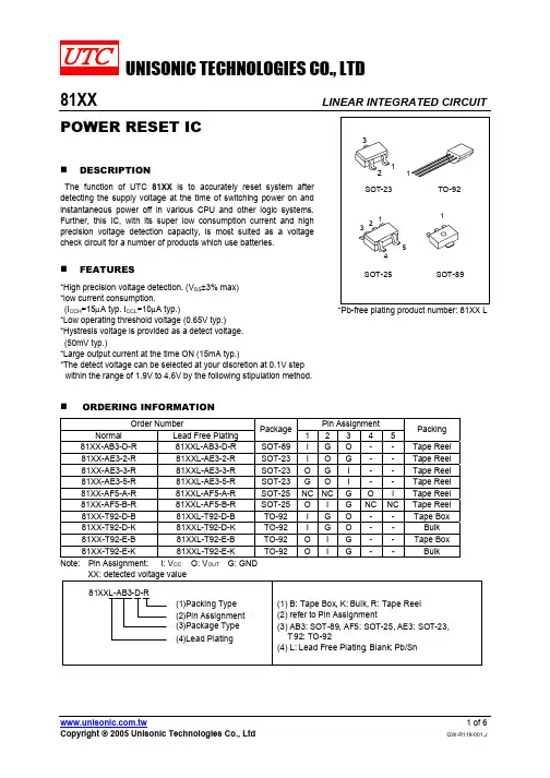
UNISONIC TECHNOLOGIES CO., LTD81XX LINEAR INTEGRATED CIRCUITPOWER RESET ICDESCRIPTIONThe function of UTC 81XX is to accurately reset system afterdetecting the supply voltage at the time of switching power on and instantaneous power off in various CPU and other logic systems. Further, this IC, with its super low consumption current and high precision voltage detection capacity, is most suited as a voltage check circuit for a number of products which use batteries.FEATURES*High precision voltage detection. (V SS ±3% max) *low current consumption.(I CCH =15µA typ. I CCL =10µA typ.)*Low operating threshold voltage (0.65V typ.)*Hystresis voltage is provided as a detect voltage. (50mV typ.)*Large output current at the time ON (15mA typ.)*The detect voltage can be selected at your discretion at 0.1V step within the range of 1.9V to 4.6V by the following stipulation method.*Pb-free plating product number: 81XX LORDERING INFORMATIONOrder Number Pin AssignmentNormal Lead Free Plating Package 12 3 4 5Packing81XX-AB3-D-R 81XXL-AB3-D-R SOT-89I G O - - Tape Reel 81XX-AE3-2-R 81XXL-AE3-2-R SOT-23I O G - - Tape Reel 81XX-AE3-3-R 81XXL-AE3-3-R SOT-23O G I - - Tape Reel 81XX-AE3-5-R 81XXL-AE3-5-R SOT-23G O I - - Tape Reel 81XX-AF5-A-R 81XXL-AF5-A-R SOT-25NC NC G O I Tape Reel 81XX-AF5-B-R 81XXL-AF5-B-R SOT-25O I G NC NC Tape Reel 81XX-T92-D-B 81XXL-T92-D-B TO-92 I G O - - Tape Box 81XX-T92-D-K 81XXL-T92-D-K TO-92 I G O - - Bulk 81XX-T92-E-B 81XXL-T92-E-B TO-92 O I G - - Tape Box 81XX-T92-E-K 81XXL-T92-E-K TO-92 O I G - - Bulk Note: Pin Assignment: I: V CC O: V OUT G: GNDMARKING INFORMATIONBLOCK DIAGRAMV CCOUTGNDThe Pin2 this product is SUB, so connect the pin to Ground.ABSOLUTE MAXIMUM RATINGSPARAMETER SYMBOL RATINGS UNITPower supply voltage V CC -0.3~+10 V Operating temperature T OPR -20~+75 °C Storage temperature T STG -40~+125 °C Note Absolute maximum ratings are those values beyond which the device could be permanently damaged.Absolute maximum ratings are stress ratings only and functional device operation is not implied.ELECTRICAL CHARACTERISTICS(Ta=25°C, The unit of resistance is Ω unless otherwise indicated.)PARAMETER SYMBOL (*1)TEST CONDITIONS MIN TYP MAX UNITUTC 8150 4.850 5.000 5.150UTC 8146 4.462 4.600 4.738UTC 8145 4.365 4.500 4.635UTC 8144 4.268 4.400 4.532UTC 8143 4.171 4.300 4.429UTC 8142 4.074 4.200 4.326UTC 8141 3.977 4.100 4.223UTC 8140 3.880 4.000 4.120UTC 8139 3.783 3.900 4.017UTC 8138 3.686 3.800 3.914UTC 8137 3.589 3.700 3.811UTC 8136 3.492 3.600 3.708UTC 8135 3.395 3.500 3.605UTC 8134 3.298 3.400 3.502UTC 8133 3.201 3.300 3.399UTC 8132 3.104 3.200 3.296UTC 8131 3.007 3.100 3.193UTC 8130 2.910 3.000 3.090UTC 8129 2.813 2.900 2.987UTC 8128 2.716 2.800 2.884UTC 8127 2.619 2.700 2.781UTC 8126 2.522 2.600 2.678UTC 8125 2.425 2.500 2.575UTC 8124 2.328 2.400 2.472UTC 8123 2.231 2.300 2.369UTC 8122 2.134 2.200 2.266UTC 8121 2.037 2.100 2.163UTC 8120 1.940 2.000 2.060UTC 8119 1.843 1.900 1.957Detection Voltage V SS 1 R L =470ΩV CC =H->L V OUT =V CCUTC 8118 1.746 1.800 1.854VHysteresis Voltage ∆V SS 1R L =470Ω, V CC =L->H->L,V OUT =V CC30 50 100 mV Detection Voltage TemperatureCoefficient V SS /∆T 1 R L =470Ω, Ta=-20~+75°C V OUT =V CC±0.01 %/°CLow Level Output Voltage V OL 1V CC =V SS min.-0.05V,R L =470Ω0.2 0.4 V Output Leakage Current I OH 2 V CC =10V , V OUT =V CC ±0.1 µA Circuit Current at ON Time I CCL 3 V CC =V SS min.-0.05V, R L =∞ 3 5 µA Circuit Current at OFF Time I CCH 3 V CC =V SS typ./0.85, R L =∞ 3 5 µAELECTRICAL CHARACTERISTICS(Cont.)PARAMETER SYMBOL (*1)TEST CONDITIONS MIN TYP MAX UNIT“H” Transmission Delay Time TpLH (*2) 4 C L =100pF, R L =4.7K Ω 20 60 µS “L” Transmission Delay Time TpHL (*3) 4 C L =100pF, R L =4.7k Ω 20 60 µSOperating Threshold Voltage V OPL 1 R L =4.7k Ω, V OL ≦0.4V 0.65 0.85 V Output current at ON Time 1 I OL 1 2R L =0, V CC =Vs min.-0.05V,V OUT =0.4V 5 mA Output current at ON Time 2 I OL 2 2 Ta=-20~+75°CR L =0, V CC =V SS min.-0.15V V OUT =0.4V3 mANote:(*1) MEASUREMENT CIRCUIT(*2) TpLH: V CC =(V SS Typ. –0.4V) -> (V SS Typ. +0.4V) (*3) TpHL: V CC =(V SS Typ. +0.4V) -> (V SS Typ. -0.4V)MEASURING CIRCUITSV 1)V CC2)V OUTV CC3)PULSE5.0V4)NOTE: 1.) A: DC AMMETER V: DC VOLTMETER CRT: OSCILLOSCOPE 2.) INPUT PULSEVsTyp. +0.4V VsTyp. -0.4V0V。
1 概述GM812X系列串口扩展芯片可为用户提供最简单和高性能的通用串口扩展方案,该系列芯片子串口最高波特率达38400bps。
该芯片提供两种工作模式,用户可根据需要灵活选择。
该芯片母串口和子串口的工作波特率可由软件调节,而不需要修改外部电路和晶振频率。
GM812X系列芯片的外部控制少,应用灵活,编程使用简单,适合于大多数需要多串口扩展的应用场合。
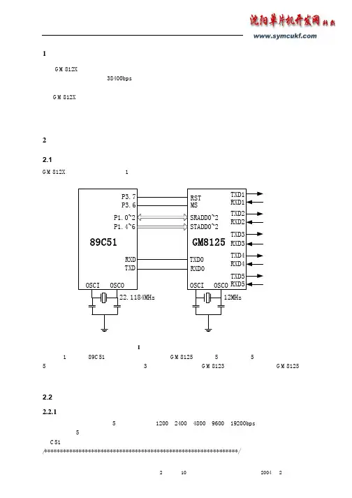
2 应用说明2.1 硬件接口GM812X系列的典型应用如图1所示:图1 典型硬件接口电路图1中选用89C51作为系统的主机,通过GM8125扩展了5个子串口,5个子串口可以与5个从机相接。
如果用户只需要扩展3个串口,则可采用GM8123,硬件连接方法和GM8125相同。
2.2 程序示例2.2.1 单通道工作模式程序示例此程序应用的环境是5个从机分别以1200、2400、4800、9600、19200bps的波特率工作,并且主机与5个从机的数据通讯采用分时的方式,即每次只对一个从机发送和接收数据。
程序以C51为例:/**************************************************************//*CPU:AT89C51 *//*晶体频率:22.1184MHz *//*机器周期:0.54uS *//*语言:C51 *//**************************************************************/#include <reg51.h>#define DELAY_TIME 60000 //Delay time/**********************I/O定义***********************/sbit MS=P3^6; //GM8125工作模式控制sbit RESET=P3^7; //GM8125复位引脚控制/******************数据变量定义*****************/unsigned char SendBuff[5]={0xaa,0x45,0x67,0xbc,0xc9};unsigned char ReceiveBuff[5]={0x00,0x00,0x00,0x00,0x00};unsigned char i=0 ,j=0 ,k=1,c=0;/*********************************************//*函数名称:delay.C *//*函数功能:延时程序*//*********************************************/void delay(unsigned int m){unsigned int n;n=0;while(n < m){n++;}return;}/******************************************************//*函数名称:MAIN.C *//*函数功能:主机主程序*//*********************************************/void main(void){TMOD = 0x20; //指定定时器1工作在方式2IE = 0x90; //开串行口中断SCON=0xc0; //串行口工作在方式3for(c=0;c<5;c++) //选择5个子串口以5种不同波特率工作{switch(c){case 0:{TH1=0xd0; //装入定时器1初值,设置工作波特率为1200bps TL1=0xd0;PCON=0x00;P1=0x11; //选择8125子通道1工作break;}case 1:{TH1 = 0xe8; //装入定时器1初值,设置工作波特率为2400bpsTL1 = 0xe8;PCON=0x00;P1=0x22; //选择8125子通道2工作break;}case 2:{TH1 = 0xf4; //装入定时器1初值,设置工作波特率为4800bpsTL1 = 0xf4;PCON=0x00;P1=0x33; //选择8125子通道3工作break;}case 3:{TH1 = 0xfa; //装入定时器1初值,设置工作波特率为9600bpsTL1 = 0xfa;PCON=0x00;P1=0x44; //选择8125子通道4工作break;}case 4:{TH1 = 0xfd; //装入定时器1初值,设置工作波特率为19200bpsTL1 = 0xfd;PCON=0x00;P1=0x55; //选择8125子通道5工作break;}default:break;}TR1=1; //启动定时器1MS=1; //GM8125工作在单通道工作模式下/*主控MCU发送/接收程序*/SBUF=SendBuff[i];while(TI==0);TI=0;i++;REN = 1;while(j!= k); //等待接收完成REN = 0; //停止接收k++;TR1=0; //T1停止}}void CommReceive(void) interrupt 4{if(RI){SBUF;ReceiveBuff[j]=RI = 0;j++;}}2.2.2 多通道工作模式程序示例此程序应用的环境是5个从机均以19200bps的波特率工作,要求主机对5个从机分别发送完数据后要等待从机向主机返回一个数据。

Installation, Maintenance& Parts ManualTable of ContentsWarnings – General Safety2. . . . . . . . . . . . . . . . . . . . . . . . . . .Introduction2 . . . . . . . . . . . . . . . . . . . . . . . . . . . . . . . . . . . . . . . Product Description3. . . . . . . . . . . . . . . . . . . . . . . . . . . . . . . . . Specifications3 . . . . . . . . . . . . . . . . . . . . . . . . . . . . . . . . . . . . . . Installation4 . . . . . . . . . . . . . . . . . . . . . . . . . . . . . . . . . . . . . . . .RequiredTools4. . . . . . . . . . . . . . . . . . . . . . . . . . . . . . . . . . .Recommended Installation Sequence4. . . . . . . . . . . . . . . . .Conveyors Up to 13 ft (3962 mm)5. . . . . . . . . . . . . . . . . . .Conveyors Longer Than 13 ft (3962 mm)5. . . . . . . . . . . . .Mounting Brackets6. . . . . . . . . . . . . . . . . . . . . . . . . . . . . . .Return Rollers7. . . . . . . . . . . . . . . . . . . . . . . . . . . . . . . . . . .Cleated Belt and 2–6¨ (51–152 mm) WideFlat Belt Conveyors7. . . . . . . . . . . . . . . . . . . . . . . . . . . .8–48¨ (203–1219 mm) WideFlat Belt Conveyors7. . . . . . . . . . . . . . . . . . . . . . . . . . . . Preventative Maintenance & Adjustment7. . . . . . . . . . . . . . . .Required Tools7. . . . . . . . . . . . . . . . . . . . . . . . . . . . . . . . . . .Standard Tools7. . . . . . . . . . . . . . . . . . . . . . . . . . . . . . . .Checklist7 . . . . . . . . . . . . . . . . . . . . . . . . . . . . . . . . . . . . . . .Lubrication 7. . . . . . . . . . . . . . . . . . . . . . . . . . . . . . . . . . . . .Maintaining Conveyor Belt 8. . . . . . . . . . . . . . . . . . . . . . . . .Troubleshooting 8. . . . . . . . . . . . . . . . . . . . . . . . . . . . . . .Cleaning 8. . . . . . . . . . . . . . . . . . . . . . . . . . . . . . . . . . . . .Conveyor Belt Replacement8. . . . . . . . . . . . . . . . . . . . . . . .Conveyor Belt Replacement Sequence 8. . . . . . . . . . . . . .Belt Removal for Conveyor WithoutStands or Gearmotor Mounting Package8. . . . . . . . . . . . . .Belt Removal for Conveyor WithStands and Gearmotor Mounting Package9. . . . . . . . . . . . .Belt Installation for Conveyor WithoutStands or Gearmotor Mounting Package9. . . . . . . . . . . . . .Belt Installation for Conveyor WithStands and Gearmotor Mounting Package10. . . . . . . . . . . .Conveyor Belt Tensioning10. . . . . . . . . . . . . . . . . . . . . . . . .Conveyor Belt Tracking11. . . . . . . . . . . . . . . . . . . . . . . . . .V – Guided Belts 11. . . . . . . . . . . . . . . . . . . . . . . . . . . . . .Non V–Guided Belts 11. . . . . . . . . . . . . . . . . . . . . . . . . . .Pulley Removal12. . . . . . . . . . . . . . . . . . . . . . . . . . . . . . . . .A–Idler Pulley Removal12. . . . . . . . . . . . . . . . . . . . . . .B–Drive Pulley Removal13. . . . . . . . . . . . . . . . . . . . . .C–Transfer Tail Pulley Removal16. . . . . . . . . . . . . . . .Bearing Replacement17. . . . . . . . . . . . . . . . . . . . . . . . . . . .Idler Bearing Replacement17. . . . . . . . . . . . . . . . . . . . . .Drive Bearing Removal and Replacement17. . . . . . . . . .Transfer Tail Pulley17. . . . . . . . . . . . . . . . . . . . . . . . . . . .Pulley Replacement17. . . . . . . . . . . . . . . . . . . . . . . . . . . . . .Idler Pulley17. . . . . . . . . . . . . . . . . . . . . . . . . . . . . . . . . .Drive Pulley17. . . . . . . . . . . . . . . . . . . . . . . . . . . . . . . . .Transfer Tail Pulley17. . . . . . . . . . . . . . . . . . . . . . . . . . . .Service Parts19 . . . . . . . . . . . . . . . . . . . . . . . . . . . . . . . . . . . . .Drive End Tail Assembly19. . . . . . . . . . . . . . . . . . . . . . . . .Transfer Tail Assembly20. . . . . . . . . . . . . . . . . . . . . . . . . . .Idler End Tail Assembly21. . . . . . . . . . . . . . . . . . . . . . . . . .Frame Assembly22. . . . . . . . . . . . . . . . . . . . . . . . . . . . . . . .–04 3” (76mm) Aluminum Side24. . . . . . . . . . . . . . . . . . . .–05 1.5” (38mm) Aluminum Side25. . . . . . . . . . . . . . . . . .–07 Low to Side Wiper26. . . . . . . . . . . . . . . . . . . . . . . . . . .–09 Low to High Side27. . . . . . . . . . . . . . . . . . . . . . . . . . .–10 .5” (13mm) Extruded Plastic28. . . . . . . . . . . . . . . . . . .–13 Adjustable Guiding29. . . . . . . . . . . . . . . . . . . . . . . . . ..5” (13mm) Cleated Guiding30. . . . . . . . . . . . . . . . . . . . . . .1” (25mm) Cleated Guiding31. . . . . . . . . . . . . . . . . . . . . . .2” (51mm) Cleated Guiding32. . . . . . . . . . . . . . . . . . . . . . .Flared Side Guiding33. . . . . . . . . . . . . . . . . . . . . . . . . . . . .Flat Belt Mounting Bracket34. . . . . . . . . . . . . . . . . . . . . . . .Cleated Belt Mounting Bracket34. . . . . . . . . . . . . . . . . . . . .Connecting Assembly without Stand Mount35. . . . . . . . . .Flat Belt Connecting Assembly withoutStand Mount35. . . . . . . . . . . . . . . . . . . . . . . . . . . . . . . . . . .Cleated Belt Connecting Assembly withoutStand Mount36. . . . . . . . . . . . . . . . . . . . . . . . . . . . . . . . . . .2” (51mm) to 6” (152mm) Flat Belt Return Roller36. . . . . .8” (203mm) to 48” (1219mm) Flat Belt Return Roller37. . .Cleated Belt Return Roller37. . . . . . . . . . . . . . . . . . . . . . . .Conveyor Belt Part Number Configuration38. . . . . . . . . . . Return Policy40 . . . . . . . . . . . . . . . . . . . . . . . . . . . . . . . . . . . . .851-512 Rev. A3200 Series End Drive Conveyor Installation, Maintenance & Parts Manual851-512 Rev. A2Dorner Mfg. Corp.IntroductionIMPORTANT: Some illustrations may showguards removed. DO NOT operate equipment with-out guards.Upon receipt of shipment:D Compare shipment with packing slip. Contact factory regarding discrepancies.D Inspect packages for shipping damage. Contact carrier regarding damage.D Accessories may be shipped loose. See accessory in-structions for installation.Dorner ’s Limited Warranty applies.Dorner 3200 series conveyors are covered by Patent Numbers 5,156,260, and corresponding patents and patent applications in other countries.Dorner reserves the right to make changes at any time without notice or obligation.Warnings – General Safety3200 Series End Drive Conveyor Installation, Maintenance & Parts ManualDorner Mfg. Corp.3851-512 Rev. ARefer to Figure 1 for typical conveyor components.A ConveyorB Gearmotor Mounting PackageC GearmotorD Guiding & AccessoriesE Mounting BracketsF Return RollersG Support StandH Variable Speed Controller I Drive EndJIdler/Tension EndTypical ComponentsFigure 1A DEEJF GHSpecificationsModels:Flat Belt 3200 Series ConveyorBelt Type*2 = Flat belt with V-guide tracking and supports3 = Flat belt with tracking cams4 = Flat belt with V –guide tracking=EnglishCleated Belt 3200 Series ConveyorCleat Spacing*=English2 = Flat belt with V-guide tracking and supports3 = Flat belt with tracking cams4 = Flat belt with V –guide tracking* See Ordering and Specifications Catalog for details.Conveyor Supports:Maximum Distances:K = 24¨ (610 mm) (Drive End)L = 12 ft (3658 mm)M = 36¨(914 mm) (Idler End)Figure 2Product Description3200 Series End Drive Conveyor Installation, Maintenance & Parts Manual851-512 Rev. A4Dorner Mfg. Corp.Specifications:NOTE: Maximum conveyor loads based on:D Non-accumulating productD Product moving towards gearmotor D Conveyor being mounted horizontal*See Ordering and Specifications Catalog for details.InstallationNOTE: Conveyor MUST be mounted straight, flatand level within confines of conveyor. Use a level (N of Figure 3) for setup.Figure 3NRequired ToolsD Hex-key wrenches:4 mm, 5 mm D LevelD Torque wrenchRecommended Installation SequenceD Install support stands (see accessory instructions)D Assemble conveyor (if required)D Attach mounting brackets to conveyor D Attach conveyor to standsD Install return rollers on conveyor (optional)DMount gearmotor mounting package (see accessory instructions)D Attach guides/accessories (see page 24 through 32 of “Service Parts ” section for details)Specifications3200 Series End Drive Conveyor Installation, Maintenance & Parts ManualDorner Mfg. Corp.5851-512 Rev. AConveyors Up to 13 ft (3962 mm)No assembly is required. Install mounting brackets and return rollers. Refer to “Mounting Brackets ” on page 6and “Return Rollers ” on page 7.Conveyors Longer Than 13 ft (3962 mm)1.Locate conveyor sections (O Figure 4)O Conveyor frame with drive end P Conveyor frame with idler end Q BeltRConnector bracketInstallation Component ListFigure 4OPRQ2.On tension end of the conveyor, identified by thepinion locking screw (S of Figure 5), push in head plate assembly (U): Loosen the pinion locking screw (S), adjust the pinion torque screw (V of Figure 6).On both sides of conveyor, loosen the two tail clamp bolts (T of Figure 5), and push head plate assembly (U) inward.Figure 5TUSFigure 6V3.Roll out conveyor belt and place conveyor framesections (O of Figure 7) into belt loop.Figure 7OO4.Join conveyor sections and install connector brack-ets (W of Figure 8) or connector/mount brackets (WA) and screws (X) on both sides as indicated.Tighten screws to 60 in-lb (7 Nm).Figure 8WXWAInstallation3200 Series End Drive Conveyor Installation, Maintenance & Parts Manual851-512 Rev. A6Dorner Mfg. Corp.NOTE: For Conveyors longer than 20 ft (6096 mm)use the process outlined in the “Conveyor Belt Ten-sioning ” section on page 10. Extend the Drive End Tail Assembly to the zero mark of the tension indica-tor (AR of Figure 9) before proceeding to step 5. The zero mark for the tension indicator is when the indi-cator begins to turn black.Figure 9AR 5.Tighten conveyor belt, refer to “Conveyor BeltTensioning ” on page 10.6.Install mounting brackets and return rollers. Refer to “Mounting Brackets ” on page 6 and “Return Roller ” on page7.Mounting Brackets1.Locate brackets. Exploded views shown in Fig-ures 10 & 11.Figure 10Mounting Brackets for Flat Belt ConveyorFigure 11Mounting Brackets for Cleated Belt Conveyor2.Remove screws (Y & Z of Figures 10 & 11), washers(AA), nuts (AB) and T-bars (AC) from brackets.3.Insert T-bars (AC of Figures 10 & 11) into conveyorside slots (AC of Figure 12). Fasten brackets (AD of Figure 12) to conveyor with mounting screws (Y).Figure 12AA Z ACYADABNOTE: Mounting brackets for flat belt conveyorsshown.4.Fasten brackets to support stand with mountingscrews (Z of Figure 12), washers (AA) and nuts (AB).5.Tighten screws (Y & Z of Figure 12) to 60 in-lb(7 Nm).Installation3200 Series End Drive Conveyor Installation, Maintenance & Parts ManualDorner Mfg. Corp.7851-512 Rev. AReturn RollersCleated Belt and 4–6¨ (51–152 mm) Wide Flat Belt Conveyors1.Locate return rollers. Exploded views shown inFigures 13 & 14.Figure 13Figure 14Return Rollers for Cleated Belt Conveyor2.Remove screws (AE of Figures 13 & 14) and clips(AF) from roller assembly.3.Install roller assemblies (AG of Figure 15) as shown.Tighten screws (AE) to 60 in-lb (7 Nm).Figure 15AEAGAG8–48¨ (203–1219 mm) Wide Flat Belt Conveyors 1.Locate return rollers. Exploded view shown inFigure 16.Figure 162.Remove screws (AH of Figure 16) and clips (AI)from roller assembly.3.Install roller assembly as shown (AJ of Figure 17).Tighten screws (AH) to 60 in-lb (7 Nm).Figure 17AHAJPreventive Maintenance and AdjustmentRequired ToolsStandard ToolsD Hex-key wrenches:2.5 mm, 4 mm, 5 mmChecklistD Keep service parts on hand (see “Service Parts ” sec-tion for recommendations)D Keep supply of belt cleaner (part # 625619)D Clean entire conveyor and knurled pulley while dis-assembledD Replace worn or damaged partsLubricationNo lubrication is required. Replace bearings if worn.Installation3200 Series End Drive Conveyor Installation, Maintenance & Parts Manual851-512 Rev. A8Dorner Mfg. Corp.Maintaining Conveyor BeltTroubleshootingInspect conveyor belt for:D Surface cuts or wear D Stalling or slipping D Damage to V-guide Surface cuts and wear indicate:D Sharp or heavy parts impacting belt D Jammed partsD Improperly installed bottom wipers (if installed)D Accumulated dirt in wipers (if installed)D Foreign material inside the conveyor D Improperly positioned accessories DBolt-on guiding is pinching beltStalling or slipping indicates:D Excessive load on beltD Conveyor belt or drive timing belt are not properly tensionedD Worn knurl or impacted dirt on drive pulley D Intermittent jamming or drive train problems Damage to V-guide indicates:D Twisted or damaged conveyor frame D Dirt impacted on pulleysD Excessive or improper side loadingNOTE: Visit for complete list oftroubleshooting solutions.CleaningIMPORTANT: Do not use belt cleaners that con-tain alcohol, acetone, Methyl Ethyl Ketone (MEK) or other harsh chemicals.Use Dorner Belt Cleaner (part # 625619). Mild soap and water may also be used. Do not soak the belt.For /05 woven polyester and /06 black anti-static belts,use a bristled brush to improve cleaning.Conveyor Belt ReplacementConveyor Belt Replacement SequenceD Remove old conveyor belt:-Conveyor without Stands or Gearmotor Mounting Package-Conveyor with Stands and Gearmotor Mounting Package D Install new conveyor belt D Tension conveyor beltBelt Removal for Conveyor Without Stands or Gearmotor Mounting Package1.If equipped, remove return rollers and guiding andaccessories from one side of conveyor.2.On tension end of the conveyor, identified by thepinion locking screw (S of Figure 18), push in head plate assembly (U): Loosen the pinion locking screw (S), adjust the pinion torque screw (V of Figure 19).On both sides of conveyor, loosen the two tail clamp bolts (T of Figure 18), and push head plate assembly (U) inward.Figure 18TUSPreventive Maintenance and Adjustment3200 Series End Drive Conveyor Installation, Maintenance & Parts ManualDorner Mfg. Corp.9851-512 Rev. AFigure 19V3.Remove conveyor belt.Belt Removal for Conveyor With Stands andGearmotor Mounting Package1.Place temporary support stands (AK of Figure 20) atboth ends of the conveyor. Place an additional support stand under the drive motor (AL), if equipped. See WARNING .Figure 20AK ALAK AMAM2.Remove mounting brackets (AM of Figure 20) fromone side of conveyor. (Reverse steps 3 & 4 of “Mounting Brackets ” section on page 6).3.If equipped, remove return rollers, guiding andaccessories from side opposite drive cover.4.On tension end of the conveyor, identified by thepinion locking screw (S of Figure 21), push in head plate assembly (U): Loosen the pinion locking screw (S), adjust the pinion torque screw (V of Figure 22).On both sides of conveyor, loosen the two tail clamp bolts (T of Figure 21), and push head plate assembly (U) inward.Figure 21TU SFigure 22V5.Remove belt (AN of Figure 23) from conveyor.Figure 23ANANBelt Installation for Conveyor without Stands or Gearmotor Mounting Package1.Orient belt so splice leading fingers (AO of Fig-ure 24) point in the direction of belt travel as identi-fied by the conveyor directional label (AP).Preventive Maintenance and Adjustment3200 Series End Drive Conveyor Installation, Maintenance & Parts Manual851-512 Rev. A10Dorner Mfg. Corp.Figure 242.Slide belt onto the conveyor frame assembly.3.Tension belt. Refer to “Conveyor Belt Tensioning ” onpage 10.4.If equipped, install wipers, return rollers and guid-ing.Belt Installation for Conveyor with Stands andGearmotor Mounting Package1.Ensure temporary support stands (AK of Figure 20)are placed at both ends of the conveyor. Place an additional support stand under the drive motor (AL),if equipped. See WARNING .2.Orient belt so splice leading fingers (AO of Fig-ure 24) point in the direction of belt travel as identi-fied by the conveyor directional label (AP).3.Install belt (AN of Figure 25) on conveyor. Liftconveyor slightly to avoid pinching belt on tempo-rary support stands.Figure 25ANAN4.Re-install conveyor mounting brackets. Refer“Mounting Brackets ” on page 6, steps 3 through 5.5.Tension belt. Refer to “Conveyor Belt Tensioning ” onpage 10.6.If equipped, re-install return rollers and guiding.Conveyor Belt TensioningNOTE: For conveyors longer than 20 ft (6096 mm)the belt tensioning proceedure outlined below may be preformed on both the Drive and Idler Ends of the conveyor.1.On tension end of the conveyor, identified by thepinion locking screw (S of Figure 26), loosen the two tail clamp bolts(T), on both sides of conveyor.Figure 26TU S2.With 5mm hex wrench, hold pinion torque screw (Vof Figure 27). Loosen the pinion locking screw (S of Figure 26) and turn the pinion torque screw(V) to extend head plate assembly.Figure 27VPreventive Maintenance and AdjustmentNOTE: On pinion gear, do not exceed a torque of 100 in-lb (11.3 N–m). Over tensioning the conveyor belt could cause excessive pulley bearing load and early failure.3.Extend head plate assembly until proper tension inthe belt is achived. If proper tensioning can not be obtained before the belt life indicator is all black (AR of Figure 28) the belt must be replaced.Figure 28AR4.After adjusting proper tensioning, tighten the pinionlocking screw (S of Figure 26) to 69 in–lbs (7.8 N–m), and tighten tail clamp bolts (T of Figure 26) on both sides of conveyor to 146 in-lb (16.5 N–m).5.If belt tracking is neccesary, refer to “Conveyor BeltTracking” on page 11.Conveyor Belt TrackingV-Guided BeltsV-guided belts do not require tracking adjustment. Non V-Guided BeltsNon V-guided belt conveyors are equipped with belt tracking assemblies.When adjusting belt tracking, always adjust the dis-charge end of the conveyor first. To adjust belt tracking: 1.Ensure tensioning racks are extended and touchingthe idler pulley headplates: loosen the pinion locking screw (S of Figure 26) and rotate the pinion torque screw (V of Figure 27) clockwise until contact with the head plate is made, then tighten the pinion locking screw (S) to 69 in–lbs (7.8 N–m)2.On the side of conveyor to be adjusted, loosen two(2) tail clamp screws(T of Figure 29).Figure 29TS3.With the conveyor running, use wrench (AS ofFigure 30) to rotate the tracking screw (A T of Figure31) in small increments until the belt tracks in thecenter of the conveyor.Figure 30ASFigure 314.Re-tighten the head plate fastening screws (T) witha 5 mm hex-key wrench to 146 in-lb (16.5 Nm).Preventive Maintenance and AdjustmentFigure 32TPulley RemovalRemove conveyor belt to access pulley(s). See “Convey-or Belt Replacement ” on page 8. Remove the desired pulley following the corresponding instructions below:D A – Idler Pulley Removal D B – Drive Pulley Removal D C – Transfer Tail Pulley RemovalA – Idler Pulley Removal1.Temporarily support the idler pulley.Figure 332.On one side of conveyor, loosen the two (2) backfastening screws (T of Figure 34) and remove two (2) front fastening screws (AU).Figure 34TAU3.Pull back the outer headplate (U of Figure 35) andremove the inner spacer (A V).Figure 35AVUAV4.Slide the idler pulley assembly (AW of Figure 36)out of the headplate on the opposite side.Figure 36AWPreventive Maintenance and Adjustment5.Remove the pulley shaft assembly: remove the clipring (AX of Figure 37) and washer (AY) from one side of the pulley assembly.Figure 37AXAY6.Slide the shaft assembly (AZ of Figure 38) out of thepulley (AW).Figure 38AZAWB –Drive Pulley Removal1.Remove the gearmotor mounting package:a – Top and Bottom Mount Packagesb – Side Mount PackagesNOTE: Bottom Mount Package shown, Top MountPackage similar.a .Top and Bottom Mount Packages1)Use a temporary support (BA of Figure 39)tosupport Gearmotor.Figure 392)Remove four (4) screws (BB of Figure 40) and remove cover (BC).Figure 40BB3)Loosen tensioner (BD of Figure 41).Figure 41BDBEPreventive Maintenance and Adjustment4)Remove taper-lock screws (BF of Figure 42) on the driven pulley (BE of Figure 41). Insert one (1) of taper lock screws (BF of Figure 42) in remaing hole (BG). Tighten screw (BF) until pulley is loose.Remove pulley, taper hub assembly and timing belt.Figure 425)Remove four (4) M5 mounting screws (BH of Figure 43) and two (2) M8 mounting screws (BI).Figure 43BIBHBJ6)Remove gearmotor and mounting plate assembly (BJ of Figure 43).b .Side Mount Package1)Temporarily support Gearmotor2)Loosen the four (4) lock screws (BK of Figure 44).Figure 443)Rotate and remove the gear motor and guard assembly (BL of Figure 45).Figure 45BL4)Remove the four (4) lock screws (BK of Figure 46) and the short side drive guard (BM).Figure 462.Loosen set screw (BN of Figure 46) and remove3–jaw coupling (BO).3.Temporarily support the drive pulley.Figure 474.Remove four shaft cover screws (BP of Figure 48).Remove the shaft cover (BQ).Preventive Maintenance and AdjustmentFigure 48BPBQ5.Loosen the bearing collar set screw (BR of Figure49) and remove bearing collar (BS). Repeat on driveshaft side of pulley (BR and BS of Figure 50).Figure 49Figure 50BRBS6.On the drive headplate, remove two (2) screws (T ofFigure 51).Figure 51T7.Remove the outer headplate assembly (BT of Figure52), and inner spacer (A V).Figure 52BTAV8.Slide the drive pulley (BU of Figure 53) out of theheadplate on the opposite side.Figure 53BUPreventive Maintenance and AdjustmentC – Transfer Tail Pulley Removal1.Temporarily support the transfer tail assembly.Figure 542.On one side of conveyor, remove the two (2) backfastening screws (T of Figure 55), and the two (2)front fastening screws (AU).Figure 55TAU3.Remove the inner spacer (A V of Figure 56).Figure 56U4.Slide the transfer tail pulley assembly (BV of Figure57) out of the headplate on the opposite side.Figure 57BV5.Remove hex nuts (BW of Figure 58).Figure 58BW6.Remove support plates (BX of Figure 59) andwashers (BY).Figure 59BXBY7.Remove pulleys (BZ of Figure 60) and additionalwashers (CA).Figure 60BZ8.To remove additonal pulleys, repeat steps 6 through7.Preventive Maintenance and AdjustmentBearing ReplacementD A– Idler BearingD B– Drive BearingD C– Transfer Tail BearingA– Idler Bearing ReplacementThe bearings in a 3200 Series Idler Pulley can not be removed. Replace the entire pulley assembly when worn.B–Drive Bearing Removal and Replacement Removal1.Turn bearing (CB of Figure 61) to align with slots(CC) in bearing housing. Then remove bearing.Figure 61CBCCReplacement1.Inspect bearing housing bearing surface. If worn ordamaged, replace. See “Service Parts” on page 19.2.Insert bearing (CB of Figure 62) into housing slot(CC). Locate anti–rotation nub (CD) to align withslot (CE), and twist bearing into housing.Figure 62CBCE CCC– Transfer Tail Bearing ReplacementThe bearings in a 3200 Series Transfer Tail Pulleycan not be removed. Replace the entire pulleyassembly when worn.Pulley ReplacementIdler PulleyTo replace the idler pulley, reverse the “Idler PulleyRemoval” proceedure on page 12.Drive PulleyTo replace the drive pulley, reverse the “Drive PulleyRemoval” proceedure on page 13.Transfer Tail PulleyTo replace the transfer tail pulley, reverse the “TransferTail Pulley Removal” proceedure on page 16. Preventive Maintenance and AdjustmentNOTE: For replacement parts other than those shown in this section, contact an authorized Dorner Service Center or the factory.Drive End Tail Assembly375813109124141561211Transfer Tail Assembly78231294141318191101761116515Idler End Assembly32136127891411510Frame Assembly4911135678102Frame LLLLL =Conveyor Length LLLL X 12 – Tail Adder # of Sections of ConveyorTail Adder =00600 for each Tension End00425for each Non –Tension EndBed Plate LLLLL = Frame LLLLL – 00013Bed Plate and Frame Formulas–04 3” (76mm) Aluminum Side2143Length FormulasLLLLL=Tail Factor =XXXX = Conveyor Length (XX.XX ft)Example17’4” End Drive Conveyor with Standard Tails Conveyor Length = 1733Tail Factor = 00200# of Sections (round up)== 1.36 = 2 SectionsLLLLL== 10298(1733 – 0100)1200(1733 x 12) – 002002–05 1.5”(38mm) Aluminum Side3214Length FormulasLLLLL=Tail Factor =XXXX = Conveyor Length (XX.XX ft)Example17’4” End Drive Conveyor with Standard Tails Conveyor Length = 1733Tail Factor = 00200# of Sections (round up)== 1.36 = 2 SectionsLLLLL== 10298(1733 – 0100)1200(1733 x 12) – 002002–07Low to Side Wiper51234Length FormulasLLLLL=Tail Factor =XXXX = Conveyor Length (XX.XX ft)Example17’4” End Drive Conveyor with Standard Tails Conveyor Length = 1733Tail Factor = 00200# of Sections (round up)== 1.36 = 2 SectionsLLLLL== 10298(1733 – 0100)1200(1733 x 12) – 002002–09Low to High Side1234Length FormulasLLLLL=Tail Factor =XXXX = Conveyor Length (XX.XX ft)Example17’4” End Drive Conveyor with Standard Tails Conveyor Length = 1733Tail Factor = 00200# of Sections (round up)== 1.36 = 2 SectionsLLLLL== 10298(1733 – 0100)1200(1733 x 12) – 002002–10 .5”(13mm) Extruded Plastic32145Length FormulasLLLLL=Tail Factor =XXXX = Conveyor Length (XX.XX ft)Example17’4” End Drive Conveyor with Standard Tails Conveyor Length = 1733Tail Factor = 00200# of Sections (round up)== 1.36 = 2 SectionsLLLLL== 10298(1733 – 0100)1200(1733 x 12) – 002002。
USB2.0 HUB控制器集成电路USB 2.0 HIGH SPEED 4-PORT HUB CONTROLLERSL2.2s数据手册Data Sheet内容目录第一章管脚分配 (3)1.1 SL2.2S管脚图 (3)1.2 SL2.2S管脚定义 (3)第二章 功能叙述 (5)2.1综述 (5)2.2指示灯 (5)2.2.1单灯方案 (5)2.2.2多灯方案 (6)2.2.3 LED指示定义 (6)2.3过流保护 (6)2.4充电支持 (6)2.5I2C接口 (7)2.6EEPROM设置 (7)第三章电气特性 (8)3.1极限工作条件 (8)3.2工作范围 (8)3.3直流电特性 (8)3.4HS/FS/LS电气特性 (8)3.5ESD特性 (8)附录一封装 (9)表格目录表格1: 端口LED定义 (6)表格 2 : ACTIVE LED定义 (6)表格3:EEPROM数据结构定义 (7)表格4: 最大额定值 (8)表格5: 工作范围 (8)表格6: 直流电特性 (8)插图目录图1:SSOP28 管脚图 (3)图2:单灯方案配置 (5)图3: 5灯方案配置 ............................................................................... (6)图 4:附录 封装图 ................................................................................... .9第一章管脚分配1.1SL2.2s管脚图图1:SSOP28 管脚图1.2SL2.2s管脚定义管脚名称28Die IO类型定义Pin#VSS 1 P 芯片地XOUT 2 O晶振PAD XIN 3 IDM4 4 B下行口4的USB信号DP4 5 BDM3 6 B下行口3的USB信号DP3 7 BDM2 8 B下行口2的USB信号DP2 9 BDM1 10 B下行口1的USB信号DP1 11 BVDD18 12 P 模拟1.8vVDD33 13 P 模拟3.3v - 14 NCUDM 15 B上行口的USB信号UDP 16 BRESET_N 17 I,Pu 芯片外部复位输入- 18 NCPSELF 19 I,Pu 高为自供电,低为总线供电VDD5 20 P 5v输入VDD33 21 P 3.3v输出DRV 22 B,Pu 点灯驱动信号LED1 23 B,Pu 点灯驱动信号LED2 24 B,Pu 点灯驱动信号PWRN 25 B,Pu 下行口电源输出控制,低有效OVCRN/SDA 26 B,PuI2C SDA数据线,内部上拉;芯片初始化完成后作为过流保护输入脚,低有效SCL 27 B,Pu I2C SCL时钟输出VDD18 28 P 数字1.8v注释:O,输出;I 输入;B 双向;P 电源/接地;Pu 上拉;Pd 下拉;NC 悬空;第二章 功能叙述2.1综述SL2.2s 是一颗高集成度,高性能,低功耗的USB2.0集线器主控芯片;该芯片采用STT 技术,单电源供电方式,芯片供电电压为5v , 内部集成5V 转3.3V,只需在外部电源添加滤波电容;芯片自带复位电路,低功耗技术让他更加出众。
CMS80F251x数据手册ArrayCMS8S78xx数据手册增强型闪存8位1T 8051微控制器Rev. 1.01请注意以下有关CMS知识产权政策*中微半导体(深圳)股份有限公司(以下简称本公司)已申请了专利,享有绝对的合法权益。
与本公司MCU或其他产品有关的专利权并未被同意授权使用,任何经由不当手段侵害本公司专利权的公司、组织或个人,本公司将采取一切可能的法律行动,遏止侵权者不当的侵权行为,并追讨本公司因侵权行为所受的损失、或侵权者所得的不法利益。
*中微半导体(深圳)股份有限公司的名称和标识都是本公司的注册商标。
*本公司保留对规格书中产品在可靠性、功能和设计方面的改进作进一步说明的权利。
然而本公司对于规格内容的使用不负责任。
文中提到的应用其目的仅仅是用来做说明,本公司不保证和不表示这些应用没有更深入的修改就能适用,也不推荐它的产品使用在会由于故障或其它原因可能会对人身造成危害的地方。
本公司的产品不授权适用于救生、维生器件或系统中作为关键器件。
本公司拥有不事先通知而修改产品的权利,对于最新的信息,请参考官方网站。
1. 产品特性1.1 功能特性◆兼容MCS-51的1T指令系统- 系统时钟频率最高支持48MHz- 机器周期最快支持1T SYS @ F SYS≤24MHz - 机器周期最快支持2T SYS @ F SYS=48MHz ◆内存- 程序FLASH:16K×8Bit- Data FLASH:1K×8Bit- 通用RAM:256×8Bit- 通用XRAM:1K×8Bit- 支持BOOT功能区,1K/2K/4K可选- 程序FLASH支持分区保护◆4种振荡方式- HSI-内部高速振荡:48MHz- HSE-外部高速振荡:8MHz/16MHz- LSE-外部低速振荡:32.768KHz- LSI-内部低速振荡:125KHz◆GPIO- 最多可达26个GPIO- 均支持上/下拉电阻功能- 均支持边沿(上升沿/下降沿/双沿)中断- 均支持唤醒功能◆中断源- 支持所有的外部端口中断- 7个定时器中断- 其它外设中断◆定时器- WDT定时器(看门狗定时器)- Timer0/1,Timer2,Timer3/4- LSE_Timer(支持休眠唤醒功能)- WUT(唤醒定时器)- BRT(串口波特率时钟发生器)◆蜂鸣器驱动- 50%占空比,频率可自由设置◆增强型PWM- 4通道增强型PWM- 4个相互独立周期计数器- 支持独立/互补/同步/成组模式- 支持边沿对齐/中心对齐方式- 支持互补模式死区延时功能- 支持刹车功能以及刹车恢复功能◆通信模块- 1xSPI(通讯速率最高可达6Mb/s)- 1xI2C(通讯速率最高可达400Kb/s)- 1xUART(波特率最高可达1Mb/s)◆工作电压范围- 2.1V~5.5V◆工作温度范围- -40℃~105℃◆低压复位功能(LVR)- 1.8V/2.0V/2.5V/3.5V◆低压检测功能(LVD)- 2.0V~4.6V 16级可选◆内置温度传感器(TS)◆高精度12位ADC- 最多可达26个AD外部通道- 参考电压可选(1.2V/2.0V/2.4V/3.0V/VDD)- 可检测内部1.2V基准电压- 支持硬件触发启动转换功能- 支持一组结果数字比较功能◆支持软件LCD驱动- 软件驱动1/3偏置- 最多支持24COM或24SEG◆支持软件LED驱动- COM SEG驱动电流可选- 最多支持26COM或26SEG◆两路模拟比较器(ACMP0/1)- 正端最多可达4种选择,负端可选内部1.2V/VDD分压- 比较器支持单边/双边迟滞- 负端内部1.2V/VDD分压可接内部ADC通道◆低功耗模式- 空闲模式(IDLE)- 休眠模式(STOP)◆支持96位唯一ID号(UID)- 每颗芯片有独立的ID号◆支持两线串行编程与调试1.2 产品对比注:(1)通过系统配置寄存器设置APROM和BOOT空间大小,APROM与BOOT空间总共最大为16K。


u Multiplex bus controls two independent buses uAux Power terminals that can be used for remote devicesuProgrammed with D5060 Handheld Programmer (not required for "i" class modules)u Operation monitoring LED uConnect to Zonex 1 or Zonex 2The D8125MUX Multiplex Bus Interface Module and associated modules are used to expand the compatible Bosch control panels beyond theirstandard number of onboard initiating zones or points.The D8125MUX module is installed in the control panel enclosure, and is connected to either Zonex 1 or Zonex 2 on the control panel where it scans themultiplex (MUX) points connected to it and reports the points’ status to the control panel. Point indexprogramming then determines if an action on the part of the control panel is required (alarm response,trouble response, and so on).FunctionsTwo Independent BusesThe multiplex bus interface can control twoindependent buses. A fault on one MUX bus does not prevent the other from operating normally.Aux Power TerminalsThe D8125MUX has Aux Power terminals labeled Power A (+,-) and Power B (+,-) that can be used for remote devices that require an uninterrupted source of power. Up to 200 mA are available at these terminals.NoticeObserve correct polarity when connecting devices to these power terminals.D5060 Hand-held ProgrammerUse the D5060 Multiplex Point Programmer to program multiplex bus points. The D5060 is not required when programming "i" class modules. In addition to programming points, use the D5060 to view the MUX device point number.Certifications and approvalsCompatible Control Panels•B9512G/B9512G-E •B8512G/B8512G-E•D9412GV4/D7412GV4/D7212GV4•D9412GV3/D7412GV3/D7212GV3•D9412GV2/D7412GV2/D7212GV2•D9412G/D7412G/D7212G•D9124 Fire Alarm Control Panel •FPD-7024 Fire Alarm Control PanelCompatibility Multiplex Modules•DS7432 Series Eight-input Remote Modules •DS7457i Series Single-zone Input Modules •DS7460i Dual-zone Input Module •DS7461i Single-zone Input Module •DS7465i Input-output ModuleCompatible Programmers •D5060 Multiplex ProgrammerWiringMaximum Wire Impedance: 33 ΩThe recommended wiring from the control panel to the module is quad (four-wire) cable. Do not use shielded or twisted-pair cable. If used in fire applications,18 AWG wire is required.Maximum Impedance: 4.05 Ω at +20°C (+68°F) nominalUse non-shielded wire for data loops. Do not exceed 75 mA on each MUX Bus output.Parts includedQuantity Component1Multiplex Bus interface 1Hardware pack 1Literature packEnvironmental ConsiderationsPropertiesPower RequirementsTrademarksAll hardware and software product names used in this document are likely to be registered trademarks and must be treated accordingly.Ordering informationD8125MUX Multiplex Bus InterfaceControls two independent buses.Order number D8125MUXRepresented by:Europe, Middle East, Africa:North America:Asia-Pacific:Bosch Security Systems B.V.P.O. Box 800025600 JB Eindhoven, The Netherlands Phone: + 31 40 2577 284****************************** Bosch Security Systems, Inc.130 Perinton ParkwayFairport, New York, 14450, USAPhone: +1 800 289 0096Fax: +1 585 223 9180*******************.comRobert Bosch (SEA) Pte Ltd, Security Systems11 Bishan Street 21Singapore 573943Phone: +65 6571 2808Fax: +65 6571 2699*****************************© Bosch Security Systems 2016 | Data subject to change without notice 2537982603 | en, V7, 20. Jul 2016。

串口扩展芯片GM8125在多功能车载移动终端中的应用曹忠成【摘要】当前,基于微处理器的嵌入式系统得到了广泛的应用,许多外围电路功能模块也具备了UART串口通讯功能,而现阶段的微处理器芯片通常只有1~2个串口,很少带有3个或3个以上的串口,很难满足多串口通讯的需要.基于此,介绍了一种1转5的串口扩展芯片GM8125,并分析了其功能特性.该方案已经成功应用到多功能车载移动终端中,并取得了满意的效果.【期刊名称】《现代电子技术》【年(卷),期】2006(029)013【总页数】3页(P132-133,136)【关键词】单片机;串口扩展;GM8125;车载终端【作者】曹忠成【作者单位】胜利油田,钻井工艺研究院,山东,东营,257017【正文语种】中文【中图分类】TN406多功能车载移动终端,主要由单片机及全球定位系统GPS模块、通用无线分组业务GPRS模块、指纹识别、汽车黑匣子等模块组成。
单片机与这些模块之间进行串行通讯,直接利用单片机的功能特点,无法满足这一需要,利用一片串口扩展芯片GM8125则可以很好地解决这个问题。
1 GM8125介绍GM8125具有将1个全双工串口扩展为5个全双工串口的功能,其封装形式有单电源和多电源之分。
多电源封装的GM8125 多用在航空等工程应用中,实际中采用的是单电源封装的GM8125 ,图1是其引脚图。
图1 GM8125引脚排列图5个子串口的波特率可调,最高可达38 400 b/s,通信协议的帧长度可调,分为10位1帧或者11位1帧两种模式。
GM8125共有6个串口,1个母串口,5个子串口,允许同时接收或者发送数据。
5个子串口分别与5个外围设备相连,母串口与单片机的串口相连,由此实现了只有1个串口的单片机与5个设备的连接。
GM8125 有3根发送地址线和3根接收地址线,用来确定数据的接收或者发送操作是发生在哪个子串口。
GM8125 扩展后,单片机向串口设备发送信息的过程如下:(1) 单片机先向地址STADD2~0 置入希望发送数据的子串口地址,再通过单片机的TXD口向母串口发送希望传输的数据。
CS1258 芯片用户手册带24bits ADC 和BIM 的高性能AFEREV0.2 通讯地址:深圳市南山区蛇口南海大道1079 号花园城数码大厦A座9楼邮政编码:518067公司电话:+(86 755)86169257传真:+(86 755)86169057公司网站:CS1258 芯片用户手册版本历史修改记录日期0.1 预览版本2016/3/15 0.2 .更新了电气特性2016/3/29.更新了典型应用图.更新了封装图目录版本历史 (2)目录 (3)图目录 (5)表目录 (5)1 简介 (6)1.1 主要特性 (6)1.2 应用场合 (6)1.3 功能说明 (6)1.4 极限值 (8)1.5 电气特性 (9)1.6 可靠性指标 (10)1.7 产品型号及引脚 (11)1.8 典型应用电路 (12)2 功能寄存器说明 (13)2.1 功能寄存器列表 (13)2.2 功能寄存器说明 (13)2.2.1 SYS —系统配置寄存器 (13)2.2.2 ADC0— ADC 配置寄存器 (14)2.2.3 ADC1— ADC 配置寄存器1 (14)2.2.4 ADC2— ADC 配置寄存器2 (15)2.2.5 ADC3— ADC 配置寄存器3 (15)2.2.6 ADC4— ADC 配置寄存器4 (16)2.2.7 ADC5— ADC 配置寄存器5 (16)2.2.8 BIM0— BIM 配置寄存器0 (17)2.2.9 BIM1— BIM 配置寄存器 (17)2.2.10 ADO— ADC 转换数据寄存器 (18)2.2.11 ADS— ADC 转换数据读取标准寄存器 (18)3 功能描述 (19)3.1 输入选择 (19)3.2 输入电平移位器 (19)3.3 IDAC1/IDAC0 和输入通道 (20)3.4 PGA 和ADC (21)3.5 数字滤波器 (23)3.5.1 频率响应 (23)3.5.2 建立时间 (23)3.6 人体阻抗测量 (25)3.6.1 正弦信号发生器 (25)3.6.2 激励电极及测量电极 (26)3.6.3 整流 (26)3.6.4 阻抗校准 (27)3.7 参考电压源 (28)3.8 内部时钟源 (28)3.9 温度传感器 (28)3.10 测量模式及其切换 (28)3.11 多种工作模式 (29)3.12 复位和断电(POR&power down) (30)4 转换有效位 (31)5 典型特性 (32)5.1 ADC 典型特性 (32)5.2 LDO/VREF 典型特性 (32)5.3 内部时钟典型特性 (32)5.4 IDAC 典型特性 (32)5.5 BIM 典型特性 (32)6 三线串行通讯接口 (37)6.1.1 读时序 (38)6.1.2 写时序 (38)7 封装 (40)图目录图 1.1 CS1258 原理框图 (7)图 1.2 CS1258 引脚图 (11)图 1.3 CS1258 典型应用电路 (12)图 3.1 模拟输入结构图 (19)图 3.2 电平移位模块 (20)图 3.3 IDAC1/IDAC0 结构及与输入通道关系 (20)图 3.4 PGA 和ADC 结构图 (21)图 3.5 COMB 滤波器的频率响应特性(Fs=331Hz,DR=10Hz,3 阶COMB) (23)图 3.6 COMB 建立过程 (24)图 3.7 BIM 模块结构图 (25)图 3.8 CS1258 低功耗工作示意图 (29)图 5.1 内部时钟全电压全温度范围的典型特性 (32)图 5.2 FWR 模式下220 欧姆纯电阻网络的测试结果 (33)图 5.3 FWR 模式下1000 欧姆纯电阻网络的测试结果 (33)图 5.4 FWR 模式下1958 欧姆纯电阻网络的测试结果 (34)图 5.5 FWR+MIX 模式510ohm+470pF 并联网络的阻抗绝对值测试结果 (34)图 5.6 FWR+MIX 模式510ohm+470pF 并联网络的相位角测试结果 (35)图 5.7 FWR+MIX 模式1018Ohm+10nF 并联网络的阻抗绝对值测试结果 (35)图 5.8 FWR+MIX 模式1018Ohm+10nF 并联网络的相位角测试结果 (36)图 6.1 读操作时序1(读AD 值) (38)图 6.2 读操作时序2(除AD 值之外的寄存器) (38)图 6.3 写操作时序 (39)图7.1 芯片LQFP32 封装尺寸信息(天水) (40)表目录表 1.1 CS1258 极限值 (8)表 1.2 CS1258 电气特性 (9)表 1.3 CS1258 引脚说明 (11)表 2.1 功能寄存器列表 (13)表 2.2 SYS 寄存器说明 (13)表 2.3 ADC0 寄存器说明 (14)表 2.4 ADC1 寄存器说明 (14)表 2.5 ADC2 寄存器说明 (15)表 2.6 ADC3 寄存器说明 (15)表 2.7 ADC4 寄存器说明 (16)表 2.8 ADC5 寄存器说明 (16)表 2.9 BIM0 寄存器说明 (17)表 2.10 BIM1 寄存器说明 (17)表 4.1 ADC 信号链不同GAIN 及DR 下的有效位(ENOB)1) (31)表 6.1 串口通讯命令列表 (37)表 6.2 三线串行通讯接口时序表 (39)版权所有,侵权必究芯海科技(深圳)股份有限公司第 5 页,共40 页1 简介1.1 主要特性◆输入●支持单端输入●支持组成多个差分输入对●支持输入电平移位功能◆PGA●1/2/4/8/16/32/64/128 倍可选增益●高达100Mohm 的等效输入阻抗◆BIM●支持4/6/8 电极测量●支持5K/10K/25K/50K/100K/250KHz 多档频率测量●支持阻抗绝对值和相角测量◆ADC●24 bit 分辨率●输出速率10~1280Hz 8 档可选◆有效位● 2.35V 参考、40Hz 速率、128 倍增益下19.5bits 有效位◆LDO 及内部参考电压●自带LDO,输出2.35/2.45/2.8/3.0V 可选,精度±1%●自带低漂移基准,内部参考电压2.048V 可选,精度±1%◆支持性能、普通、低功耗、休眠模式◆支持电压测量、温度测量、BIM 测量及手动测量模式,单命令切换◆低漂移片上时钟◆三线串行通讯1.2 应用场合桥式传感器四角平衡称重压力检测人体阻抗分析交流测脂1.3 功能说明CS1258 原理框图如图1 所示。
TPS8125 6 SLVSAZ93-W,高效率的升压转换器中MicroSiP™包装检查样品:TPS81256特点∙在4MHz运行效率91%∙宽V∙我≥ 550毫安在V OUT = 5.0V,V IN ≥ 3.3V∙±2%总直流电压精度∙43μA电源电流∙最好的一流的电压和负载瞬态∙V IN ≥至五输出操作∙低纹波轻载PFM模式∙真正的负载断开在关机期间∙热关断及过载保护∙分1毫米简介解决方案∙整体解决方案尺寸<9毫米2∙9针MicroSiP 商标包装应用∙手机,智能手机,平板电脑∙单声道和立体声演艺学院应用∙U SB-OTG功能,HDMI应用∙U SB充电接口(5V)图1。
效率与负载电流描述TPS8125x器件是的完整MicroSiP™的DC / DC升压用于电池供电的便携式应用的电源解决方案。
包中包含的开关稳压器,电感器和输入/输出电容器。
只有一个很小的额外的输出电容要求完成设计。
TPS8125x是基于高频率同步升压型DC / DC转换为电池供电的便携式应用而优化。
该DC / DC转换器工作在规定的4 MHz的开关频率,并进入省电模式在轻负载电流在整个负载电流范围内保持高效率的运作。
PFM模式扩展电池寿命,电源电流降低至43 μ A(典型值)在轻负荷运行。
TPS8125x支持低功耗应用的目的,一个完整的锂离子电池电压范围超过3W的输出功率。
在关机模式下的输入电流小于1μA(典型值),从而最大限度地延长电池寿命。
TPS8125x提供的比9毫米非常小解决方案尺寸,由于外部元件的最低金额。
在紧凑低调(2.6毫米x2.9毫米)(1.0MM)BGA封装标准的表面贴装设备的自动化装配合适的解决方案打包。
图2。
最小解决方案尺寸的应用请注意,一个重要的通知有关可用性,标准保修,并使用在关键应用德州仪器公司的半导体产品和免责条款及其出现在此数据表的结束。
MicroSiP是德州仪器的商标。
除非另有说明,本文件包含版权所有©2012年,德州仪器生产数据信息为出版日期。
元器件交易网ContentsFeatures (1)Applications (1)Pin Assignment (1)Block Diagram (1)Selection Guide (2)Absolute Maximum Ratings (2)Electrical Characteristics (3)Test Circuits (11)Technical Terms (12)Operation (13)Transient Response (14)Standard Circuit (17)Application Circuits (17)Notes on Design (19)Dimensions (20)Markings (20)Package Power Dissipation (21)Taping Dimensions (22)Characteristics (25)Measuring Circuits (31)Frequently Asked Question s (32)Seiko Instruments Inc.1The S-812XXSG Series is a three-terminal positive voltage regulator made using the CMOS process. Since the S-812XXSG Series has higher precision output voltage and consumes less current than existing three-terminal voltage regulators, battery-powered portable equipment can have a higher performance and a longer service life.ApplicationsConstant voltage power supply of battery-powered equipment, communications equipment, video equipmentand othersPin AssignmentHIGH-PRECISIONVOLTAGE REGULATORS-812XXSG SeriesFeaturesLow power consumption (2.5 A max.) High accuracy of output voltage±2% : V OUT 2.7 V ±2.4% : V OUT 2.6 VSmall input/output voltage difference(S-81250SG: 160 mV typ. I OUT =10 mA) Low temperature coefficient of output voltage(S-81250SG: ±0.625 mV/ C typ.) Wide operating voltage range(S-81250SG: 16 V max.) Good line regulation(S-81250SG: 40 mV typ. I OUT =1 A to 40 mA) T O-92, SOT-89-3 and SOT-23-5 packageBlock DiagramFigure 1R LGNDV INV OUT2+-*Ref.vol.31* Parasitic diodeBottom view123(1)TO-921GND 2V IN 3V OUTTop view1231GND 2V IN 3V OUT(2)SOT-89-3GNDV IN V OUTNC NCTop View (3)SOT-23-5Figure 2HIGH PRECISION VOLTAGE REGULATOR S-812XXSG Series2Seiko Instruments Inc.Selection GuideTable 1Output voltage TO-92 *1SOT-89-3 *2SOT-23-5 *21.1 2.4%S-81211SGY-X S-81211SGUP-DQA-X S-81211SG-QA-X 1.5 2.4%S-81215SGY-XS-81215SGUP-DQK-XS-81215SG-QK-X 1.7 2.4%S-81217SG-QQ-X 1.8 2.4%S-81218SG-QR-X 2.0 2.4%S-81220SGY-X S-81220SGUP-DQS-X S-81220SG-QS-X 2.1 2.4%S-81221SGUP-DQU-X 2.3 2.4%S-81223SGY-X S-81223SG-QW-X 2.4 2.4%S-81224SGY-X S-81224SGUP-DQX-X S-81224SG-QX-X 2.5 2.4%S-81225SGY-X S-81225SGUP-DQH-X S-81225SG-QH-X 2.7 2.0%S-81227SGUP-DQZ-X 3.0 2.0%S-81230SGY-X S-81230SGUP-DQB-X S-81230SG-QB-X 3.3 2.0%S-81233SGY-X S-81233SGUP-DQF-X S-81233SG-QF-X 3.5 2.0%S-81235SGY-X S-81235SGUP-DQI-X S-81235SG-QI-X 3.6 2.0%S-81236SGUP-DQ7-X 3.7 2.0%S-81237SGY-X S-81237SGUP-DQE-X S-81237SG-QE-X 4.0 2.0%S-81240SGY-X S-81240SGUP-DQJ-X S-81240SG-QJ-X 4.2 2.0%S-81242SG-IB-X 4.5 2.0%S-81245SGY-X S-81245SGUP-DQ5-X S-81245SG-Q5-X 4.6 2.0%S-81246SGY-X S-81246SGUP-DQM-X S-81246SG-QM-X 4.7 2.0%S-81247SG-IE-X 5.0 2.0%S-81250SGY-X S-81250SGUP-DQD-X S-81250SG-QD-X 5.2 2.0%S-81252SGY-XS-81252SGUP-DQL-X S-81252SG-QL-X5.3 2.0%S-81253SGUP-DIJ-X 5.4 2.0%S-81254SGUP-DIK-X 5.5 2.0%S-81255SGUP-DIL-X 5.6 2.0%S-81256SGUP-DIM-X*1In the TO-92 package, “x” differs depending upon the packaging form:B : Loose T, Z : Tape*2In the SOT package, “x” differs depending upon the packaging form (in the SOT-23-5 package, on-tape packed products only):S : StickT : Tape (T1 and T2 are available depending upon the direction of the IC)Absolute Maximum RatingsTable 2(Unless otherwise specified: Ta=25 C)ParameterSymbol Conditions Ratings Unit V OUT 2.6 V 12V Input voltage V IN V OUT 2.7 V18Output voltage V OUT V IN +0.3 to V SS -0.3V Output current I OUT 100mA TO-92400Power dissipation P D SOT-89-3500mW SOT-23-5150Operating temperature T opr -40 to +85 C Storage temperatureT stg-40 to +125CCaution: Keep static electricity to a minimum.HIGH-PRECISION VOLTAGE REGULATORS-812XXSG SeriesSeiko Instruments Inc.3Electrical Characteristics1.S-81211SGY-X, S-81211SGUP-DQA-X, S-81211SG-QA-X (1.1-V output type)Parameter Symbol ConditionsMin.Typ.Max.Unit Test cir.Output voltage V OUT V IN =1.5 V, I OUT =0.5 mA 1.073 1.100 1.127V 1I/O voltage difference V dif I OUT =0.5 mA 0.050.2V 1Line regulation 1 V OUT 1V IN =1.5 to 10 V I OUT =0.5 mA 1050mV 1Line regulation 2 V OUT 2V IN =1.5 to 10 V I OUT =10 A1077mV 1Load regulation V OUT 3V IN =1.5 VI OUT =10 A to 0.5 mA 10100mV 1Current consumption I SS V IN =1.5 V, Unloaded1.22.5 A 2Input voltage V IN 10V Temperature charac-teristic of V OUTV OUT TaV IN =1.5 V, I OUT = 0.5 mA Ta=-40 C to 85 C±0.138mV/ C2. S-81215SGY-X, S-81215SGUP-DQK-X, S-81215SG-QK-X (1.5-V output type)Parameter Symbol ConditionsMin.Typ.Max.Unit Test cir.Output voltage V OUT V IN =3.5 V, I OUT =0.5 mA 1.464 1.500 1.536V 1I/O voltage difference V dif I OUT =0.5 mA 0.030.18V 1Line regulation 1 V OUT 1V IN =2.5 to 10 V I OUT =0.5 mA 739mV 1Line regulation 2 V OUT 2V IN =2.5 to 10 V I OUT =1 A7105mV 1Load regulation V OUT 3V IN =3.5 VI OUT =1 A to10 mA 80120mV 1Current consumption I SS V IN =3.5 V, Unloaded1.22.5 A 2Input voltage V IN 10V Temperature charac-teristic of V OUTV OUT TaV IN =3.5 V, I OUT = 0.5 mA Ta=-40 C to 85 C±0.188mV/ C3. S-81217SG-QQ-X (1.7-V output type)Parameter Symbol ConditionsMin.Typ.Max.Unit Test cir.Output voltage V OUT V IN =3.7 V, I OUT =10 mA 1.659 1.700 1.741V 1I/O voltage difference V dif I OUT =10 mA 0.77 1.63V 1Line regulation 1 V OUT 1V IN =2.7 to 10 V I OUT =1 mA 843mV 1Line regulation 2 V OUT 2V IN =2.7 to 10 V I OUT =1 A8119mV 1Load regulation V OUT 3V IN =3.7 VI OUT =1 A to 10 mA 80120mV 1Current consumption I SS V IN =3.7 V, Unloaded1.22.5 A 2Input voltage V IN 10V Temperature charac-teristic of V OUTV OUT TaV IN =3.7 V, I OUT = 10 mA Ta=-40 C to 85 C±0.213mV/ CTable 3(Unless otherwise specified: Ta=25 C)Table 4(Unless otherwise specified: Ta=25 C)Table 5(Unless otherwise specified: Ta=25 C)HIGH PRECISION VOLTAGE REGULATOR S-812XXSG Series4Seiko Instruments Inc.4.S-81218SG-QR-X (1.8-V output type)Parameter Symbol ConditionsMin.Typ.Max.Unit Test cir.Output voltage V OUT V IN =3.8 V, I OUT =10 mA 1.756 1.800 1.843V 1I/O voltage difference V dif I OUT =10 mA 0.72 1.55V 1Line regulation 1 V OUT 1V IN =2.8 to 10 V I OUT =1 mA 845mV 1Line regulation 2 V OUT 2V IN =2.8 to 10 V I OUT =1 A8126mV 1Load regulation V OUT 3V IN =3.8 VI OUT =1 A to 10 mA 80120mV 1Current consumption I SS V IN =3.8 V, Unloaded1.22.5 A 2Input voltage V IN 10V Temperature charac-teristic of V OUTV OUT TaV IN =3.8 V, I OUT = 10 mA Ta=-40 C to 85 C±0.225mV/ C5.S-81220SGY-X, S-81220SGUP-DQS-X, S-81220SG-QS-X (2.0-V output type)Parameter Symbol ConditionsMin.Typ.Max.Unit Test cir.Output voltage V OUT V IN =4.0 V, I OUT =10 mA 1.592 2.000 2.048V 1I/O voltage difference V dif I OUT =10 mA 0.63 1.39V 1Line regulation 1 V OUT 1V IN =3.0 to 10 V I OUT =1 mA 848mV 1Line regulation 2 V OUT 2V IN =3.0 to 10 V I OUT =1 A8140mV 1Load regulation V OUT 3V IN =4.0 VI OUT =1 A to 10 mA 80120mV 1Current consumption I SS V IN =4.0 V, Unloaded1.22.5 A 2Input voltage V IN 10V Temperature charac-teristic of V OUTV OUT TaV IN =4.0 V, I OUT = 10 mA Ta=-40 C to 85 C±0.250mV/ C6.S-81221SGUP-DQU-X (2.1-V output type)Parameter Symbol ConditionsMin.Typ.Max.Unit Test cir.Output voltage V OUT V IN =4.1 V, I OUT =10 mA 2.049 2.100 2.151V 1I/O voltage difference V dif I OUT =10 mA 0.59 1.32V 1Line regulation 1 V OUT 1V IN =3.1 to 10 V I OUT =1 mA 950mV 1Line regulation 2 V OUT 2V IN =3.1 to 10 V I OUT =1 A9147mV 1Load regulation V OUT 3V IN =4.1 VI OUT =1 A to 10 mA 80120mV 1Current consumption I SS V IN =4.1 V, Unloaded1.22.5 A 2Input voltage V IN 10V Temperature charac-teristic of V OUTV OUT TaV IN =4.1 V, I OU T = 10 mA Ta=-40 C to 85 C±0.263mV/ CTable 6(Unless otherwise specified : Ta=25 C)Table 7(Unless otherwise specified : Ta=25 C)Table 8(Unless otherwise specified : Ta=25 C)HIGH-PRECISION VOLTAGE REGULATORS-812XXSG SeriesSeiko Instruments Inc.57.S-81223SGY-X, S-81223SG-QW-X (2.3-V output type)Parameter Symbol ConditionsMin.Typ.Max.Unit Test cir.Output voltage V OUT V IN =4.3 V, I OUT =10 mA2.244 2.300 2.356V 1I/O voltage difference V dif IOUT =10 mA0.53 1.20V 1Line regulation 1 V OUT 1V IN =3.3 to 10 V I OUT =1 mA 954mV 1Line regulation 2 V OUT 2V IN =3.3 to 10 V I OUT =1 A9161mV 1Load regulation V OUT 3V IN =4.3 VI OUT =1 A to 10 mA 80120mV 1Current consumption I SS V IN =4.3 V, Unloaded1.22.5 A 2Input voltage V IN 10V Temperature charac-teristic of V OUTV OUT TaV IN =4.3 V, I OUT = 10 mA Ta=-40 C to 85 C±0.288mV/ C8.S-81224SGY-X, S-81224SGUP-DQX-X, S-81224SG-QX-X (2.4-V output type)Parameter Symbol ConditionsMin.Typ.Max.Unit Test cir.Output voltage V OUT V IN =4.4 V, I OUT =10 mA 2.342 2.400 2.458V 1I/O voltage difference V dif I OUT =10 mA 0.49 1.15V 1Line regulation 1 V OUT 1V IN =3.4 to 10 V I OUT =1 mA 1055mV 1Line regulation 2 V OUT 2V IN =3.4 to 10 V I OUT =1 A10168mV 1Load regulation V OUT 3V IN =4.4 VI OUT =1 A to 10 mA 80120mV 1Current consumption I SS V IN =4.4 V, Unloaded1.22.5 A 2Input voltage V IN 10V Temperature charac-teristic of V OUTV OUT TaV IN =4.4 V, I OUT = 10 mA Ta=-40 C to 85 C±0.300mV/ C9.S-81225SGY-X, S-81225SGUP-DQH-X, S-81225SG-QH-X (2.5-V output type)Parameter Symbol ConditionsMin.Typ.Max.Unit Test cir.Output voltage V OUT V IN =4.5 V, I OUT =10 mA 2.440 2.500 2.560V 1I/O voltage difference V dif I OUT =10 mA 0.59 1.32V 1Line regulation 1 V OUT 1V IN =3.5 to 10 V I OUT =1 mA 1057mV 1Line regulation 2 V OUT 2V IN =3.5 to 10 V I OUT =1 A10175mV 1Load regulation V OUT 3V IN =4.5 VI OUT =1 A to 10 mA 80120mV 1Current consumption I SS V IN =4.5 V, Unloaded1.22.5 A 2Input voltage V IN 10V Temperature charac-teristic of V OUTV OUT TaV IN =4.5 V, I OUT = 10 mA Ta=-40 C to 85 C±0.313mV/ CTable 9(Unless otherwise specified : Ta=25 C)Table 10(Unless otherwise specified : Ta=25 C)Table 11(Unless otherwise specified : Ta=25 C)HIGH-PRECISION VOLTAGE REGULATOR S-812XXSG Series6Seiko Instruments Inc.10.S-81227SGUP-DQZ-X (2.7-V output type)Parameter Symbol ConditionsMin.Typ.Max.Unit Test cir.Output voltage V OUT V IN =4.7 V, I OUT =10 mA 2.646 2.700 2.754V 1I/O voltage difference V dif I OUT =10 mA 0.52 1.20V 1Line regulation 1 V OUT 1V IN =3.7 to 16 V I OUT =1 mA 3672mV 1Line regulation 2 V OUT 2V IN =3.7 to 16 V I OUT =1 A36189mV 1Load regulation V OUT 3V IN =4.7 VI OUT =1 A to 20 mA 80120mV 1Current consumption I SS V IN =4.7 V, Unloaded1.22.5 A 2Input voltage V IN 16V Temperature charac-teristic of V OUTV OUT TaV IN =4.7 V, I OUT = 10 mA Ta=-40 C to 85 C±0.338mV/ C11.S-81230SGY-X, S-81230SGUP-DQB-X, S-81230SG-QB-X (3.0-V output type)Parameter Symbol ConditionsMin.Typ.Max.Unit Test cir.Output voltage V OUT V IN =5.0 V, I OUT =10 mA 2.940 3.000 3.060V 1I/O voltage difference V dif I OUT =10 mA 0.44 1.04V 1Line regulation 1 V OUT 1V IN =4.0 to 16 V I OUT =1 mA 3978mV 1Line regulation 2 V OUT 2V IN =4.0 to 16 V I OUT =1 A39210mV 1Load regulation V OUT 3V IN =5 VI OUT =1 A to 20 mA 60100mV 1Current consumption I SS V IN =5.0 V, Unloaded1.22.5 A 2Input voltage V IN 16V Temperature charac-teristic of V OUTV OUT TaV IN =5.0 V, I OUT = 10 mA Ta=-40 C to 85 C±0.375mV/ C12.S-81233SGY-X, S-81233SGUP-DQF-X, S-81233SG-QF-X (3.3-V output type)Parameter Symbol ConditionsMin.Typ.Max.Unit Test cir.Output voltage V OUT V IN =5.3 V, I OUT =10 mA 3.234 3.300 3.366V 1I/O voltage difference V dif I OUT =10 mA 0.370.91V 1Line regulation 1 V OUT 1V IN =4.3 to 16 V I OUT =1 mA 4284mV 1Line regulation 2 V OUT 2V IN =4.3 to 16 V I OUT =1 A42231mV 1Load regulation V OUT 3V IN =5.3 VI OUT =1 A to 20 mA 60100mV 1Current consumption I SS V IN =5.3 V, Unloaded1.22.5 A 2Input voltage V IN 16V Temperature charac-teristic of V OUTV OUT TaV IN =5.3 V, I OUT = 10 mA Ta=-40 C to 85 C±0.413mV/ CTable 12(Unless otherwise specified : Ta=25 C)Table 13(Unless otherwise specified : Ta=25 C)Table 14(Unless otherwise specified : Ta=25 C)HIGH-PRECISION VOLTAGE REGULATORS-812XXSG SeriesSeiko Instruments Inc.713.S-81235SGY-X, S-81235SGUP-DQI-X, S-81235SG-QI-X (3.5-V output type)Parameter Symbol ConditionsMin.Typ.Max.Unit Test cir.Output voltage V OUT V IN =5.5 V, I OUT =10 mA 3.430 3.500 3.570V 1I/O voltage difference V dif I OUT =10 mA 0.340.84V 1Line regulation 1 V OUT 1V IN =4.5 to 16 V I OUT =1 mA 4488mV 1Line regulation 2 V OUT 2V IN =4.5 to 16 V I OUT =1 A44245mV 1Load regulation V OUT 3V IN =5.5 VI OUT =1 A to 30 mA 60100mV 1Current consumption I SS V IN =5.5 V, Unloaded1.22.5 A 2Input voltage V IN 16V Temperature charac-teristic of V OUTV OUT TaV IN =5.5 V, I OUT = 10 mA Ta=-40 C to 85 C±0.438mV/ C14. S-81236SGUP-DQ7-X (3.6-V output type)Parameter Symbol ConditionsMin.Typ.Max.Unit Test cir.Output voltage V OUT V IN =5.6 V, I OUT =10 mA 3.528 3.600 3.672V 1I/O voltage difference V dif I OUT =16 mA 0.320.81V 1Line regulation 1 V OUT 1V IN =4.6 to 16 V I OUT =1 mA 4590mV 1Line regulation 2 V OUT 2V IN =4.6 to 16 V I OUT =1 A45252mV 1Load regulation V OUT 3V IN =5.6 VI OUT =1 A to 30 mA 60100mV 1Current consumption I SS V IN =5.6 V, Unloaded1.22.5 A 2Input voltage V IN 16V Temperature charac-teristic of V OUTV OUT TaV IN =5.6 V, I OUT = 10 mA Ta=-40 C to 85 C±0.450mV/ C15.S-81237SGY-X, S-81237SGUP-DQE-X, S-81237SG-QE-X (3.7-V output type)Parameter Symbol ConditionsMin.Typ.Max.Unit Test cir.Output voltage V OUT V IN =5.7 V, I OUT =10 mA 3.626 3.700 3.774V 1I/O voltage difference V dif I OUT =10 mA 0.310.78V 1Line regulation 1 V OUT 1V IN =4.7 to 16 V I OUT =1 mA 4692mV 1Line regulation 2 V OUT 2V IN =4.7 to 16 V I OUT =1 A46259mV 1Load regulation V OUT 3V IN =5.7 VI OUT =1 A to 30 mA 60100mV 1Current consumption I SS V IN =5.7 V, Unloaded1.22.5 A 2Input voltage V IN 16V Temperature charac-teristic of V OUTV OUT TaV IN =5.7 V, I OUT = 10 mA Ta=-40 C to 85 C±0.463mV/ CTable 15(Unless otherwise specified : Ta=25 C)Table 17(Unless otherwise specified : Ta=25 C)Table 16(Unless otherwise specified : Ta=25 C)HIGH-PRECISION VOLTAGE REGULATOR S-812XXSG Series8Seiko Instruments Inc.16.S-81240SGY-X, S-81240SGUP-DQJ-X, S-81240SG-QJ-X (4.0-V output type)Parameter Symbol ConditionsMin.Typ.Max.Unit Test cir.Output voltage V OUT V IN =6.0 V, I OUT =10 mA 3.920 4.000 4.080V 1I/O voltage difference V dif I OUT =10 mA 0.270.70V 1Line regulation 1 V OUT 1V IN =5.0 to 16 V I OUT =1 mA 4896mV 1Line regulation 2 V OUT 2V IN =5.0 to 16 V I OUT =1 A48280mV 1Load regulation V OUT 3V IN =6.0 VI OUT =1 A to 30 mA 5090mV 1Current consumption I SS V IN =6.0 V, Unloaded1.22.5 A 2Input voltage V IN 16V Temperature charac-teristic of V OUTV OUT TaV IN =6.0 V, I OUT = 10 mA Ta=-40 C to 85 C±0.500mV/ C17. S-81242SG-IB-X (4.2-V output type)Parameter Symbol ConditionsMin.Typ.Max.Unit Test cir.Output voltage V OUT V IN =6.2V, I OUT =10 mA 4.116 4.200 4.284V 1I/O voltage difference V dif I OUT =10 mA 0.240.65V 1Line regulation 1 V OUT 1V IN =5.2 to 16 V I OUT =1 mA 50100mV 1Line regulation 2 V OUT 2V IN =5.2 to 16 V I OUT =1 A50294mV 1Load regulation V OUT 3V IN =6.2 VI OUT =1 A to 30 mA 5090mV 1Current consumption I SS V IN =6.2 V, Unloaded1.22.5 A 2Input voltage V IN 16V Temperature charac-teristic of V OUTV OUT TaV IN =6.2 V, I OUT = 10 mA Ta=-40 C to 85 C±0.525mV/ C18.S-81245SGY-X, S-81245SGUP-DQ5-X, S-81245SG-Q5-X (4.5-V output type)Parameter Symbol ConditionsMin.Typ.Max.Unit Test cir.Output voltage V OUT V IN =6.5 V, I OUT =10 mA 4.410 4.500 4.590V 1I/O voltage difference V dif I OUT =10 mA 0.210.58V 1Line regulation 1 V OUT 1V IN =5.5 to 16 V I OUT =1 mA 52104mV 1Line regulation 2 V OUT 2V IN =5.5 to 16 V I OUT =1 A52315mV 1Load regulation V OUT 3V IN =6.5 VI OUT =1 A to 30 mA 5090mV 1Current consumption I SS V IN =6.5 V, Unloaded1.22.5 A 2Input voltage V IN 16V Temperature charac-teristic of V OUTV OUT TaV IN =6.5 V, I OUT = 10 mA Ta=-40 C to 85 C±0.563mV/ CTable 18(Unless otherwise specified : Ta=25 C)Table 20(Unless otherwise specified : Ta=25 C)Table 19(Unless otherwise specified : Ta=25 C)HIGH-PRECISION VOLTAGE REGULATORS-812XXSG SeriesSeiko Instruments Inc.919.S-81246SGY-X, S-81246SGUP-DQM-X, S-81246SG-QM-X (4.6-V output type)Parameter Symbol ConditionsMin.Typ.Max.Unit Test cir.Output voltage V OUT V IN =6.6 V, I OUT =10 mA 4.508 4.600 4.692V 1I/O voltage difference V dif I OUT =10 mA 0.200.57V 1Line regulation 1 V OUT 1V IN =5.6 to 16 V I OUT =1 mA 53105mV 1Line regulation 2 V OUT 2V IN =5.6 to 16 V I OUT =1 A53322mV 1Load regulation V OUT 3V IN =6.6 VI OUT =1 A to 30 mA 5090mV 1Current consumption I SS V IN =6.6 V, Unloaded1.22.5 A 2Input voltage V IN 16V Temperature charac-teristic of V OUTV OUT TaV IN =6.6 V, I OUT = 10 mA Ta=-40 C to 85 C±0.575mV/ C20.S-81247SG-IE-X (4.7-V output type)Parameter Symbol ConditionsMin.Typ.Max.Unit Test cir.Output voltage V OUT V IN =6.7 V, I OUT =10 mA 4.606 4.700 4.794V 1I/O voltage difference V dif I OUT =10 mA 0.190.55V 1Line regulation 1 V OUT 1V IN =5.7 to 16 V I OUT =1 mA 54107mV 1Line regulation 2 V OUT 2V IN =5.7 to 16 V I OUT =1 A54329mV 1Load regulation V OUT 3V IN =6.7 VI OUT =1 A to 30 mA 5090mV 1Current consumption I SS V IN =6.7 V, Unloaded1.22.5 A 2Input voltage V IN 16V Temperature charac-teristic of V OUTV OUT TaV IN =6.7 V, I OUT = 10 mA Ta=-40 C to 85 C±0.588mV/ C21.S-81250SGY-X, S-81250SGUP-DQD-X, S-81250SG-QD-X (5.0-V output type)Parameter Symbol ConditionsMin.Typ.Max.Unit Test cir.Output voltage V OUT V IN =7.0 V, I OUT =10 mA 4.900 5.000 5.100V 1I/O voltage difference V dif I OUT =10 mA 0.160.50V 1Line regulation 1 V OUT 1V IN =6.0 to 16 V I OUT =1 mA 55110mV 1Line regulation 2 V OUT 2V IN =6.0 to 16 V I OUT =1 A55350mV 1Load regulation V OUT 3V IN =7.0 VI OUT =1 A to 40 mA 4080mV 1Current consumption I SS V IN =7.0 V, Unloaded1.22.5 A 2Input voltage V IN 16V Temperature charac-teristic of V OUTV OUT TaV IN =7.0 V, I OUT = 10 mA Ta=-40 C to 85 C±0.625mV/ CTable 21(Unless otherwise specified : Ta=25 C)Table 22(Unless otherwise specified : Ta=25 C)Table 23(Unless otherwise specified : Ta=25 C)22.S-81252SGY-X, S-81252SGUP-DQL-X, S-81252SG-QL-X (5.2-V output type)Parameter Symbol Conditions Min.Typ.Max.Unit Testcir.Output voltage V OUT V IN =7.2 V, I OUT =10 mA 5.096 5.200 5.304V1 I/O voltage difference V dif I OUT=10 mA 0.150.47V1 Line regulation 1 V OUT1V IN =6.2 to 16 VI OUT=1 mA57113mV1Line regulation 2 V OUT2V IN =6.2 to 16 VI OUT=1 A57364mV1Load regulation V OUT3V IN =7.2 VI OUT=1 A to 40 mA4080mV1 Current consumption I SS V IN =7.2 V, Unloaded 1.2 2.5 A2 Input voltage V IN 16VTemperature charac-teristic of V OUT V OUTTaV IN=7.2 V, I OUT = 10 mATa=-40 C to 85 C±0.650 mV/ C23.S-81253SGUP-DIJ-X (5.3-V output type)Parameter Symbol Conditions Min.Typ.Max.Unit Testcir.Output voltage V OUT V IN =7.3 V, I OUT =10 mA 5.194 5.300 5.406V1 I/O voltage difference V dif I OUT=10 mA 0.140.45V1 Line regulation 1 V OUT1V IN =6.3 to 16 VI OUT=1 mA57114mV1Line regulation 2 V OUT2V IN =6.3 to 16 VI OUT=1 A57371mV1Load regulation V OUT3V IN =7.3 VI OUT=1 A to 40 mA4080mV1 Current consumption I SS V IN =7.3 V, Unloaded 1.2 2.5 A2 Input voltage V IN 16VTemperature charac-teristic of V OUT V OUTTaV IN=7.3 V, I OUT = 10 mATa=-40 C to 85 C±0.663 mV/ C24.S-81254SGUP-DIK-X (5.4-V output type)Parameter Symbol Conditions Min.Typ.Max.Unit Testcir.Output voltage V OUT V IN =7.4 V, I OUT =10 mA 5.292 5.400 5.508V1 I/O voltage difference V dif I OUT=10 mA 0.130.44V1 Line regulation 1 V OUT1V IN =6.4 to 16 VI OUT=1 mA58115mV1Line regulation 2 V OUT2V IN =6.4 to 16 VI OUT=1 A58378mV1Load regulation V OUT3V IN =7.4 VI OUT=1 A to 40 mA4080mV1 Current consumption I SS V IN =7.4 V, Unloaded 1.2 2.5 A2 Input voltage V IN 16VTemperature charac-teristic of V OUT V OUTTaV IN=7.4 V, I OUT = 10 mATa=-40 C to 85 C±0.675 mV/ CTable 24(Unless otherwise specified: Ta=25 C)Table 25(Unless otherwise specified: Ta=25 C)Table 26(Unless otherwise specified: Ta=25 C)25.S-81255SGUP-DIL-X (5.5-V output type)Parameter Symbol Conditions Min.Typ.Max.Unit Testcir.Output voltage V OUT V IN =7.5 V, I OUT =10 mA 5.390 5.500 5.610V 1 I/O voltage difference V dif I OUT=10 mA 0.130.43V1 Line regulation 1 V OUT1V IN =6.5 to 16 VI OUT=1 mA58116mV1Line regulation 2 V OUT2V IN =6.5 to 16 VI OUT=1 A58385mV1Load regulation V OUT3V IN =7.5 VI OUT=1 A to 40 mA4080mV1 Current consumption I SS V IN =7.5 V, Unloaded 1.2 2.5 A2 Input voltage V IN 16VTemperature charac-teristic of V OUT V OUTTaV IN=7.5 V, I OUT = 10 mATa=-40 C to 85 C±0.688 mV/ C26.S-81256SGUP-DIM-X (5.6-V output type)Parameter Symbol Conditions Min.Typ.Max.Unit Testcir.Output voltage V OUT V IN =7.6 V, I OUT =10 mA 5.488 5.600 5.712V1 I/O voltage difference V dif I OUT=10 mA 0.120.42V1 Line regulation 1 V OUT1V IN =6.6 to 16 VI OUT=1 mA59117mV1Line regulation 2 V OUT2V IN =6.6 to 16 VI OUT=1 A59392mV1Load regulation V OUT3V IN =7.6 VI OUT=1 A to 40 mA4080mV1 Current consumption I SS V IN =7.6 V, Unloaded 1.2 2.5 A2 Input voltage V IN 16VTemperature charac-teristic of V OUT V OUTTaV IN=7.6 V, I OUT = 10 mATa=-40 C to 85 C±0.7 mV/ CTest CircuitsTable 27(Unless otherwise specified: Ta=25 C)Table 28(Unless otherwise specified: Ta=25 C)Figure 3GND GNDV IN V OUTV IN V OUT12S-812XXSGSeriesV V AVA S-812XXSGSeriesTechnical Terms1Output voltage (V OUT)The precision of output voltage is guaranteed at ±2.0% or ±2.4% under the prescribed conditions of input voltage, output voltage, and temperature, which differ with items. If these conditions are varied, output voltage value may change into beyond the scope of precision of output voltage. See electrical characteristics and characteristicsdata for detail.2Line regulations 1 and 2 ( V OUT1, V OUT2)Indicates the input voltage dependencies of output voltage. That is, the values express how the output voltage changes, when input voltage is changed under the condition that output current is fixed.3Load regulation ( V OUT3)Indicates the output current dependencies of output voltage. That is, the values express how the output voltage changes, when output current is changed under the condition that input voltage is fixed.4I/O voltage defference (V dif)98% of V OUT is output when the voltage of V OUT+V dif is applied. When V dif is small, output keeps a constantvoltage in the small side of input voltage and large output current can be obtained.NOTE : V dif is highly dependent on I OUT.Operation1Basic operationFigure 4 shows the block diagram of the S-812XXSG Series.The error amplifier compares a reference voltage V REF with a part of the output voltage fed back by the feedback resistors R A and R B . It supplies the control transistor with the gate current, necessary to keep a stable output voltage range not influenced by input voltage or temperature fluctuation.V INError amplifierR BR ACurrent source-+V OUTGND*Reference voltage circuit* Parasitic diodeFigure 4 Reference block diagram2Internal circuit2.1Reference voltage circuitIn a voltage regulator, the reference voltage circuit plays a very important role because any change will show up directly at an output.The S-812XXSG Series has 0.8 V typical stable voltage circuit as a highly stable reference voltage source.Features:Low power consumptionGood temperature characteristic2.2Error amplifierThe error amplifier consumes very low current because it is a differential amplifier in a stable current circuit.Features:Good matching characteristics Wide operating voltage range Low offset voltage2.3Control transistorThe S-812XXSG Series has a Pch MOS transistor as a current control transistor shown in Figure 6. Therefore an output current I OUT is expressed by the following formula where is only a small difference between input and output voltages:I OUT =KP{2(V GS -V TP ) (V IN -V OUT )-(V IN -V OUT )2}*KP :Conductive coefficiencyV TP :Threshold voltage of a control transistor Setting KP to the large value results in a voltage regulator with 160 mV typical I/O voltage difference.V IN -V IN +GNDV INV OUTFigure 5 Error amplifierBiasV INV OUTGNDV GSV REF -+** Parasitic diodeFigure 6 Control transistorNOTE :A parasitic diode is generated between V IN and V OUT .If the electric potential of V IN is higher than that of V OUT , IC may break because of a reverse current.Keep V OUT less than V IN +0.3 V.3Temperature characteristic of output voltageThe temperature characteristic of the output voltage is expressed by the following formula in the range of -40 C to 85 C.*V REF is 0.7 V min., 0.8 V typ., 0.9 V max.Transient Response1.Line transient responseThe overshoot and undershoot are caused in the output voltage if the input voltage fluctuates while the output current is constant. Figure 7 shows the output voltage fluctuation due to input voltage change between 6.0 V and 10 V in square wave. Table 19 shows the parameter dependency when input voltage fluctuates. For reference,Figure 8 describes the measurement circuit.Table 29 Parameter dependency due to input voltage fluctuationParameterMethod to decreaseovershootMethod to decreaseundershootOutput currentI OUTDecrease Decrease Load capacitance C L Increase Increase Input voltage fluctuation V IN *DecreaseDecrease TemperatureTaHigh temperature*V IN : High voltage value - low voltage valueFor reference, the next page describes the results of measuring the ringing amounts at the V OUT pin using theoutput current (I OUT ), load capacitance (C L ), input voltage fluctuation width ( V IN ), and temperature as parameters.V REFV OUT x (±0.1) mV/ C typ.Figure 7 Output voltage fluctuation due to input voltage fluctuationInput voltage6.010 VUndershootOvershootOutput voltageFigure 8 Measuring circuitFast amplifierP.G.S-812XXSGOscilloscopeC LV OUTV SSV IN+-- 2.Load transient responseThe overshoot and undershoot are caused in the output voltage if the output current fluctuates while the inputvoltage is costant. Figure 9 shows the output voltage fluctuation due to output current change between 10mA and 1 A in square wave. Table 20 shows the parameter dependency when output current fluctuates. For reference,Figure 10 describes the measuring circuit.Line transient response of S-81250SGReference data1.I OUT dependencyC L =10 F Ta=25 C1.21.00.80.60.40.20.0051015202530Ringing amount(V)I OUT (mA)2.C L dependencyUndershoot OvershootI OUT =10mA Ta=25 C1.21.00.80.60.40.20.00Ringing amount(V)1020304050C L ( F)4.Temperature dependencyUndershoot OvershootI OUT =10mA C L =10 F1.21.00.80.60.40.20.0Ringing amount(V)80400-40Ta ( C)3. V IN dependencyV IN shows the difference between the low voltage fixed to 6 V and the high voltage.For example, V IN = 2 V means the difference between 6 V and 8 V. 1.21.00.80.60.40.20.0Ringing amount(V)1245V IN (V)3C L =10 F Ta=25 CI OUT =10mAFigure 9 Output voltage fluctuation due to output current fluctuationOutput current10mA1 AOutput voltageOvershootUndershootFigure 10 Measuring circuitS-812XXSGOscilloscopeC LV OUT V SSV IN。
techniqueFicheInjecteur T8125CA24V60WPour les installations en24V CAL'alimentation par Ethernet(PoE)offre une solution simple,rapide etéconomique pour alimenter les produits réseau. Un injecteur transmet l'alimentation et les données au périphérique réseau avec PoE intégré.Il n'est pas nécessaire de remplacer les commutateurs et les infrastructures de câblage Ethernet.L'injecteur AXIS T8125CA24V60W est un injecteurà1port qui se brancheàune source d'alimentation de24V CA.Il fournit60W(deux fois IEEE802.3at), une puissance nécessaire lorsqu'il s'agit d'utiliser des caméras réseau AXIS Q60-E Network Camerasàdes températures inférieuresà-20°C(-4°F).C'est une solutionéconomique,puisque le système n'a pas besoin de câbles d'alimentation et d'adaptateur mural secteur.>IEEE802.3at>24V CA>Prise en charge des dômes PTZ Axis>Installation prêteàl'emploiInjecteur T8125CA24V60WInjecteursFonction Les données et l'alimentation sont acheminées vers un produit devidéo sur IP par un câble EthernetÀutiliser avec un diviseur PoE pour un produit de vidéo sur IPsans prise en charge intégrée de PoEDébit de données10/100/1000Mbit/sInstallation et gestion Détecte automatiquement les périphériques PoE et High PoE et fournit une alimentation en ligneAffichage de la gestion des voyants LED locauxDonnées et alimentationAlimentation Alimentation haute puissance par Ethernet,max.60WEntrée Tension d'entrée CA:24V CA+/-20%(max.80W)Fréquence CA:50–60HzSortie55V CC,(max.60W)Connecteurs Câble RJ45blindé,normes EIA568A et568BConnecteur d'alimentation pour terminal CAà2brochesCâblage Données fournies sur les paires1/2et3/6pour10/100Ethernet, sur les quatre paires pour Gigabit EthernetAlimentation sur les paires1/2(-),3/6(+),4/5(+)et7/8(-)GénéralDéveloppementDurableSans PVCÉcran etindicateursLes LED se situent sur le panneau avantVoyant CA:voyant d’alimentationDEL du port:connectivitédes donnéesMontage Mur,étagère ou rail DIN aConditionsd'utilisationÀ30W:-10°Cà40°C(14°Fà104°F)-10°Cà50°C(14°Fà122°F)Humiditémaximale relative de95%(sans condensation) Homologations RoHS,REACH,WEEE,CE,EN55022Classe B,EN55024,FCC Partie15Sous-partie B Classe B,VCCI Classe B,RCM AS/NZS CISPR22Classe B,KCC KN22Classe B,KN24,IEC/EN/UL60950-1,GS,CBDimensions43x84x166mm(1,7x3,3x6,5po)Poids450g(1lb)AccessoiresfournisGuide d'installationAXIS Connector A2-pin5.08StraightAccessoires enoptionAXIS Midspan DIN Clip APour plus d'accessoires,voir Garantie Garantie de3ans,voir /warrantya.Vendu comme accessoire en optionResponsabilitéenvironnementale:/environmental-responsibility©2013-2020Axis Communications AB.AXIS COMMUNICATIONS,AXIS et VAPIX sont des marques déposées d’Axis AB ou encours de dépôt par Axis AB dans différentes juridictions.Tous les autres noms,produits ou services sont la propriétéde leursdétenteurs respectifs.Document sujetàmodification sans préavis.T10067425/FR/M3.3/2010。
RF Power Field Effect TransistorsN-Channel Enhancement-Mode Lateral MOSFETsDesigned for GSM and GSM EDGE base station applications with frequencies from 1800 to 2000 MHz. Can be used in Class AB and Class C for all typical cellular base station modulations.GSM Application•Typical GSM Performance: V DD = 28 Volts, I DQ = 1100 mA, P out =125Watts CW, f = 1930 MHz.Power Gain — 16.5 dB Drain Efficiency — 55%GSM EDGE Application•Typical GSM EDGE Performance: V DD = 28 Volts, I DQ = 1100 mA,P out = 57 Watts Avg., Full Frequency Band (1930-1990 MHz).Power Gain — 17 dB Drain Efficiency — 39%Spectral Regrowth @ 400 kHz Offset = -60 dBc Spectral Regrowth @ 600 kHz Offset = -74 dBc EVM — 2.6% rms•Capable of Handling 5:1 VSWR, @ 28 Vdc, 1960 MHz, 125 Watts CW Output Power•Typical P out @ 1 dB Compression Point ] 140 Watts CW Features•Characterized with Series Equivalent Large-Signal Impedance Parameters •Internally Matched for Ease of Use •Integrated ESD Protection •RoHS Compliant•In Tape and Reel. R3 Suffix = 250 Units per 56 mm, 13 inch Reel .Table 1. Maximum RatingsRatingSymbol Value Unit Drain-Source Voltage V DSS -0.5, +65Vdc Gate-Source Voltage V GS -6.0, +10Vdc Operating VoltageV DD 32, +0Vdc Storage Temperature Range T stg -65 to +150°C Case Operating Temperature T C 150°C Operating Junction Temperature (1,2)T J225°CTable 2. Thermal CharacteristicsCharacteristicSymbol Value (2,3)Unit Thermal Resistance, Junction to Case Case Temperature 81°C, 125 W CW Case Temperature 81°C, 71 W CWR θJC0.310.35°C/W1.Continuous use at maximum temperature will affect MTTF.2.MTTF calculator available at /rf. Select Software & Tools/Development Tools/Calculators to access MTTF calculators by product.3.Refer to AN1955, Thermal Measurement Methodology of RF Power Amplifiers. Go to /rf. Select Documentation/Application Notes - AN1955.Document Number: MRF7S18125BHRev. 0, 11/2008Freescale Semiconductor Technical DataMRF7S18125BHR3 MRF7S18125BHSR3Table 3. ESD Protection CharacteristicsTest MethodologyClass Human Body Model (per JESD22-A114)1B (Minimum)Machine Model (per EIA/JESD22-A115) A (Minimum)Charge Device Model (per JESD22-C101)IV (Minimum)Table 4. Electrical Characteristics (T C = 25°C unless otherwise noted)CharacteristicSymbolMinTypMaxUnitOff CharacteristicsZero Gate Voltage Drain Leakage Current (V DS = 65 Vdc, V GS = 0 Vdc)I DSS ——10μAdc Zero Gate Voltage Drain Leakage Current (V DS = 28 Vdc, V GS = 0 Vdc)I DSS ——1μAdc Gate-Source Leakage Current (V GS = 5 Vdc, V DS = 0 Vdc)I GSS——1μAdcOn CharacteristicsGate Threshold Voltage(V DS = 10 Vdc, I D = 316 μAdc)V GS(th) 1.2 1.9 2.7Vdc Gate Quiescent Voltage(V DS = 28 Vdc, I D = 1100 mAdc)V GS(Q)— 2.7—Vdc Fixture Gate Quiescent Voltage (1)(V DD = 28 Vdc, I D = 1100 mAdc, Measured in Functional Test)V GG(Q)4 5.37Vdc Drain-Source On-Voltage(V GS = 10 Vdc, I D = 3.16 Adc)V DS(on)0.10.20.3VdcDynamic Characteristics (1)Reverse Transfer Capacitance(V DS = 28 Vdc ± 30 mV(rms)ac @ 1 MHz, V GS = 0 Vdc)C rss — 1.15—pF Output Capacitance(V DS = 28 Vdc ± 30 mV(rms)ac @ 1 MHz, V GS = 0 Vdc)C oss —673—pF Input Capacitance(V DS = 28 Vdc, V GS = 0 Vdc ± 30 mV(rms)ac @ 1 MHz)C iss—309—pFFunctional Tests (In Freescale Test Fixture, 50 ohm system) V DD = 28 Vdc, I DQ = 1100 mA, P out = 125 W CW, f = 1930 MHzPower Gain G ps 1516.518dB Drain Efficiency ηD 5155—%Input Return LossIRL—-12-7dB1.V GG = 2 x V GS(Q). Parameter measured on Freescale Test Fixture, due to resistive divider network on the board. Refer to Test Circuit schematic.2.Part internally matched both on input and output.(continued)MRF7S18125BHR3 MRF7S18125BHSR3Table 4. Electrical Characteristics (T C = 25°C unless otherwise noted) (continued)CharacteristicSymbol Min Typ Max Unit Typical Performances (In Freescale Test Fixture, 50 ohm system) V DD = 28 Vdc, I DQ = 1100 mA, 1930-1990 MHz BandwidthP out @ 1 dB Compression PointP1dB —140—W IMD Symmetry @ 125 W PEP , P out where IMD Third Order Intermodulation ` 30 dBc(Delta IMD Third Order Intermodulation between Upper and Lower Sidebands > 2 dB)IMD sym—10—MHzVBW Resonance Point(IMD Third Order Intermodulation Inflection Point)VBW res —35—MHz Gain Flatness in 60 MHz Bandwidth @ P out = 125 W CW G F — 1.02—dB Average Deviation from Linear Phase in 60 MHz Bandwidth @ P out = 125 W CWΦ— 3.3—°Average Group Delay @ P out = 125 W CW, f = 1960 MHz Delay — 2.49—ns Part-to-Part Insertion Phase Variation @ P out = 125 W CW, f = 1960 MHz, Six Sigma Window ΔΦ— 6.7—°Gain Variation over Temperature (-30°C to +85°C)ΔG —0.016—dB/°C Output Power Variation over Temperature (-30°C to +85°C)ΔP1dB—0.01—dBm/°CTypical GSM EDGE Performances (In Freescale GSM EDGE Test Fixture, 50 ohm system) V DD = 28 Vdc, I DQ = 1100 mA, P out = 57 W Avg., 1930-1990 MHz EDGE Modulation Power Gain G ps —17—dB Drain Efficiency ηD —39—%Error Vector MagnitudeEVM — 2.6—% rms Spectral Regrowth at 400 kHz Offset SR1—-60—dBc Spectral Regrowth at 600 kHz OffsetSR2—-74—dBcMRF7S18125BHR3 MRF7S18125BHSR3Figure 1. MRF7S18125BHR3(HSR3) Test Circuit SchematicZ80.200″ x 0.083″ Microstrip Z9 1.045″ x 0.083″ Microstrip Z100.071″ x 0.083″ Microstrip Z110.227″ x 0.083″ Microstrip Z121.280″ x 0.080″ Microstrip Z13, Z140.760″ x 0.080″ MicrostripPCBTaconic TLX-8 RF35, 0.031″, εr = 2.55Z10.227″ x 0.083″ Microstrip Z20.697″ x 0.083″ Microstrip Z30.618″ x 0.083″ Microstrip Z40.568″ x 1.000″ Microstrip Z50.092″ x 1.000″ Microstrip Z60.095″ x 1.000″ Microstrip Z70.565″ x 1.000″ MicrostripTable 5. MRF7S18125BHR3(HSR3) Test Circuit Component Designations and ValuesPartDescriptionPart NumberManufacturer C11 μF, 50 V Chip Capacitor 12065G105AT2A AVX C2, C3, C4, C5 4.7 μF, 50 V Chip CapacitorsGRM55ER71H475KA01L Murata C6220 μF, 63 V Electrolytic Chip Capacitor 2222 136 68221Vishay C7, C8, C9, C10, C11 6.8 pF Chip Capacitors ATC100B6R8BT500XT ATC C12, C131 pF Chip Capacitors ATC100B1R0BT500XT ATC C14, C15, C16, C17, C180.2 pF Chip Capacitors ATC100B0R2BT500XT ATC R1, R210 k Ω, 1/4 W Chip Resistors CRCW12061001FKEA Vishay R310 Ω, 1/4 W Chip ResistorCRCW120610R1FKEAVishayFigure 2. MRF7S18125BHR3(HSR3) Test Circuit Component LayoutMRF7S18125BHR3 MRF7S18125BHSR3MRF7S18125BHR3 MRF7S18125BHSR3TYPICAL CHARACTERISTICSP out , OUTPUT POWER (WATTS) CW100131817151410300Figure 5. Power Gain versus Output PowerG p s , P O W E R G A I N (d B )161000.110TWO−TONE SPACING (MHz)Figure 6. Intermodulation Distortion Productsversus Two-Tone Spacing1MRF7S18125BHR3 MRF7S18125BHSR3TYPICAL CHARACTERISTICS60P in , INPUT POWER (dBm)53515034373552363839Figure 7. Pulsed CW Output Power versusInput PowerP o u t , O U T P U T P O W E R (d B c )54555657404142433001815103020P out , OUTPUT POWER (WATTS) CWFigure 8. Power Gain and Drain Efficiencyversus Output PowerG p s , P O W E R G A I N (d B )17.51710040585916.51615.51514.51413.51325354550556065E V M , E R R O R V E C T O R M A G N I T U D E (% r m s )063142)P out , OUTPUT POWER (WATTS)20Figure 11. Spectral Regrowth at 400 kHzversus Output Power S P E C T R A L R E G R O W T H @ 400 k H z (d B c )4020060801001201401601803350P out , OUTPUT POWER (WATTS)20Figure 12. Spectral Regrowth at 600 kHzversus Output Power402006080100120140160180ηD , D R A I N E F F I C I E N C Y (%)MRF7S18125BHR3 MRF7S18125BHSR3TYPICAL CHARACTERISTICSP out , OUTPUT POWER (WATTS) AVG.500122420160101820604030010Figure 13. EVM and Drain Efficiency versusOutput PowerE V M , E R R O R V E C T O R M A G N I T U D E (% r m s )141918171615f, FREQUENCY (MHz)Figure 14. Power Gain versus FrequencyG p s , P O W E R G A I N (d B )41005025010990T J , JUNCTION TEMPERATURE (°C)Figure 15. MTTF versus Junction TemperatureThis above graph displays calculated MTTF in hours when the device is operated at V DD = 28 Vdc, P out = 125 W CW, and ηD = 55%.MTTF calculator available at /rf. Select Software & Tools/Development Tools/Calculators to access MTTF calculators by product.107106105110130150170190M T T F (H O U R S )2102301081930194019501960197019801990ηD , D R A I N E F F I C I E N C Y (%)MRF7S18125BHR3 MRF7S18125BHSR3GSM TEST SIGNALFigure 16. EDGE Spectrum−10−20−30−40−50−60−70−80−90−100200 kHzSpan 2 MHzCenter 1.96 GHz−110(d B )MRF7S18125BHR3 MRF7S18125BHSR3Z o = 5ΩZ loadZ sourcef = 2040MHzf = 1880MHzf = 1880MHzf = 2040MHzV DD = 28 Vdc, I DQ = 1100 mA, P out = 125 W CWfMHzZ sourceWZ loadW1880 1.31 - j3.61 1.32 - j3.061900 1.25 - j3.061.30 - j2.921920 1.21 - j3.30 1.28 - j2.791940 1.17 - j3.17 1.26 - j2.671960 1.13 - j3.06 1.23 - j2.551980 1.10 - j2.92 1.20 - j2.422000 1.06 - j2.83 1.18 - j2.3020200.99 - j2.75 1.16 - j2.1820400.91 - j2.66 1.12 - j2.07Z source=Test circuit impedance as measured fromgate to ground.Z load=Test circuit impedance as measuredfrom drain to ground.Figure 17. Series Equivalent Source and Load ImpedanceZ source Z loadOutputMatchingNetwork分销商库存信息:FREESCALEMRF7S18125BHR3MRF7S18125BHR5MRF7S18125BHSR3 MRF7S18125BHSR5。
D-Link™ DES-1250GWeb Smart 48-Port 10/100Mbps+2-Port Combo 10/100/1000Mbps Copper/SFP(Mini GBIC) Gigabit SwitchManualFirst EditionBuilding Networks for PeopleRECYCLABLEInformation in this document is subject to change without notice.© 2004 D-Link Computer Corporation. All rights reserved.Reproduction in any manner whatsoever without the written permission of D-Link Computer Corporation is strictly forbidden.Trademarks used in this text: D-Link and the D-LINK logo are trademarks of D-Link Computer Corporation; Microsoft and Windows are registered trademarks of Microsoft Corporation.Other trademarks and trade names may be used in this document to refer to either the entities claiming the marks and names or their products. D-Link Computer Corporation disclaims any proprietary interest in trademarks and trade names other than its own.FCC WarningThis equipment has been tested and found to comply with the limits for a Class A digital device, pursuant to Part 15 of the FCC Rules. These limits are designed to provide reasonable protection against harmful interference when the equipment is operated in a commercial environment. This equipment generates, uses, and can radiate radio frequency energy and, if not installed and used in accordance with this user’s guide, may cause harmful interference to radio communications. Operation of this equipment in a residential area is likely to cause harmful interference in which case the user will be required to correct the interference at his own expense.CE Mark WarningThis is a Class A product. In a domestic environment, this product may cause radio interference in which case the user may be required to take adequate measures.Warnung!Dies ist ein Produkt der Klasse A. Im Wohnbereich kann dieses Produkt Funkstoerungen verursachen. In diesem Fall kann vom Benutzer verlangt werden, angemessene Massnahmen zu ergreifen.Precaución!Este es un producto de Clase A. En un entorno doméstico, puede causar interferencias de radio, en cuyo case, puede requerirse al usuario para que adopte las medidas adecuadas.Attention!Ceci est un produit de classe A. Dans un environnement domestique, ce produit pourrait causer des interférences radio, auquel cas l`utilisateur devrait prendre les mesures adéquates.Attenzione!Il presente prodotto appartiene alla classe A. Se utilizzato in ambiente domestico il prodotto può causare interferenze radio, nel cui caso è possibile che l`utente debba assumere provvedimenti adeguati.VCCI WarningTABLE OF CONTENTAbout This Guide (4)Purpose (4)Terms/Usage (4)Introduction (5)Gigabit Ethernet Technology (5)Fast Ethernet Technology (5)Switching Technology (5)VLAN (Virtual Local Area Network) (6)Features (7)Unpacking and Installation (8)Unpacking (8)Installation (8)Rack Mounting (8)Connecting Network Cable (8)AC Power (9)Identifying External Components (10)Front Panel (10)Rear Panel (10)Understanding LED Indicators (11)Power and System LEDs (11)Ports 1~48 10/100M Status LEDs (11)Ports 49~50 Gigabit Status LEDs (11)Ports 49~ 50 mini-GBIC Status LEDs (12)Configuration (13)Installing the Web Management Utility (13)Discovery List (13)Monitor List (14)Device Setting (14)Toolbar (15)Configuring the Switch (16)Login (16)Setup Menu (17)Configuring Setup Setting (17)Port Settings (17)VLAN Settings (Virtual Local Area Network) (18)Trunk Setting (19)Device Status (19)Statistic (19)System Setting (20)Trap Setting (21)Set Password (21)Backup Setting (21)Reset Setting (22)Logout (22)ABOUT THIS GUIDECongratulations on your purchase of the Web Smart 48+2G-Port 10/100/1000Mbps/SFP Switch. This device integrates 1000Mbps Gigabit Ethernet, 100Mbps Fast Ethernet, and 10Mbps Ethernet network capabilities in a highly flexible package.PurposeThis guide discusses how to install your Web Smart 48+2G-Port 10/100/1000Mbps/SFP Switch.Terms/UsageIn this guide, the term “Switch” (first letter upper case) refers to your Web Smart 48+2G-Port 10/100/1000Mbps Switch, and “switch” (first letter lower case) refers to other Ethernet switches.INTRODUCTIONThis chapter describes the features of the Web-Smart 48+2G-Port 10/100/1000Mbps/SFP Switch and some background information about Ethernet/Fast Ethernet/Gigabit Ethernet switching technology.Gigabit Ethernet TechnologyGigabit Ethernet is an extension of IEEE 802.3 Ethernet utilizing the same packet structure, format, and support for CSMA/CD protocol, full-duplex, flow control, and management objects, but with a tenfold increase in theoretical throughput over 100-Mbps Fast Ethernet and a hundredfold increase over 10-Mbps Ethernet. Since it is compatible with all 10-Mbps and 100-Mbps Ethernet environments, Gigabit Ethernet provides a straightforward upgrade without wasting a company’s existing investment in hardware, software, and trained personnel.The increased speed and extra bandwidth offered by Gigabit Ethernet are essential to coping with the network bottlenecks that frequently develop as computers and their busses get faster and more users use applications that generate more traffic. Upgrading key components, such as your backbone and servers to Gigabit Ethernet can greatly improve network response times as well as significantly speed up the traffic between your subnets.Gigabit Ethernet enables fast optical fiber connections to support video conferencing, complex imaging, and similar data-intensive applications. Likewise, since data transfers occur 10 times faster than Fast Ethernet, servers outfitted with Gigabit Ethernet NIC’s are able to perform 10 times the number of operations in the same amount of time.In addition, the phenomenal bandwidth delivered by Gigabit Ethernet is the most cost-effective method to take advantage of today and tomorrow’s rapidly improving switching and routing internetworking technologies. With expected advances in the coming years in silicon technology and digital signal processing that will enable Gigabit Ethernet to eventually operate over unshielded twisted-pair (UTP) cabling, outfitting your network with a powerful 1000-Mbps-capable backbone/server connection creates a flexible foundation for the next generation of network technology products.Fast Ethernet TechnologyThe growing importance of LANs and the increasing complexity of desktop computing applications are fueling the need for high performance networks. A number of high-speed LAN technologies have been proposed to provide greater bandwidth and improve client/server response times. Among them, 100BASE-T (Fast Ethernet) provides a non-disruptive, smooth evolution from the current 10BASE-T technology. The non-disruptive and smooth evolution nature, and the dominating potential market base, virtually guarantees cost-effective and high performance Fast Ethernet solutions.100Mbps Fast Ethernet is a standard specified by the IEEE 802.3 LAN committee. It is an extension of the 10Mbps Ethernet standard with the ability to transmit and receive data at 100Mbps, while maintaining the CSMA/CD Ethernet protocol. Since the 100Mbps Fast Ethernet is compatible with all other 10Mbps Ethernet environments, it provides a straightforward upgrade and takes advantage of the existing investment in hardware, software, and personnel training.Switching TechnologyAnother approach to pushing beyond the limits of Ethernet technology is the development of switching technology. A switch bridges Ethernet packets at the MAC address level of the Ethernet protocol transmitting among connected Ethernet or Fast Ethernet LAN segments.Switching is a cost-effective way of increasing the total network capacity available to users on a local area network. A switch increases capacity and decreases network loading by dividing a local area network into different segments, which do not compete with each other for network transmission capacity.The switch acts as a high-speed selective bridge between the individual segments. The switch, without interfering with any other segments, automatically forwards traffic that needs to go from one segment to another. By doing this the total network capacity is multiplied, while still maintaining the same network cabling and adapter cards.Switching LAN technology is a marked improvement over the previous generation of network bridges, which were characterized by higher latencies. Routers have also been used to segment local area networks, but the cost of a router, the setup and maintenance required make routers relatively impractical. Today switches are an ideal solution to most kinds of local area network congestion problems.VLAN (Virtual Local Area Network)A VLAN is a group of end-stations that are not constrained by their physical location and can communicate as if a common broadcast domain, a LAN. The primary utility of using VLAN is to reduce latency and the need for routers, by using faster switching instead. Other VLAN utility includes:Security, Security is increased with the reduction of opportunity in eavesdropping on a broadcast network because data will be switched to only those confidential users within the VLAN.Cost Reduction, VLANs can be used to create multiple broadcast domains, thus eliminating the need of expensive routers.Port-based (or port-group) VLAN is the common method of implementing a VLAN, and is the one supplied in the Switch.Features48×10/100Mbps Auto-negotiation Fast Ethernet RJ-45 ports2×10/100/1000Mbps Auto-negotiation Gigabit RJ-45 ports2×mini-GBIC/SFP ports, share with the 2 gigabit copper portsAll RJ-45 ports support auto MDI/MDIX, so there is no need to use cross-over cables or an up-link port Half-duplex transfer mode for 10/100Mbps RJ45 portsFull-duplex transfer mode for 10/100/1000Mbps RJ45 portsStore-and-Forward switching scheme capability to support rate adaptation and ensure data integrityUp to 4K unicast addresses entities per device, self-learning, and table aging1536KBytes packet bufferSupports IEEE 802.3x flow control for full-duplex mode portsSupports Back-pressure flow control for half-duplex mode portsSupports 802.1Q VLANSupports Port-base QoSSupports seven Port-base Trunking groupSupports Port MirroringSupports Port-setting for Speed/Disable, Flow controlEasy configuration via Web BrowserEasy setting via Web Management UtilityStandard 19” Rack-mount sizeUNPACKING AND INSTALLATIONThis chapter provides unpacking and installation information for the Switch.UnpackingOpen the shipping cartons of the Switch and carefully unpacks its contents. The carton should contain the following items:One Web Smart 48+2G-Port 10/100/1000Mbps/SFP SwitchOne AC power cord, suitable for your area’s electrical power connectionsFour rubber feet to be used for shock cushioningScrews and two mounting bracketsCD-Rom with Web Management Utility and User’s GuideIf any item is found missing or damaged, please contact your local reseller for replacement.InstallationThe site where you install the hub stack may greatly affect its performance. When installing, consider the following pointers:Install the Switch in a fairly cool and dry place. See Technical Specifications for the acceptable temperature and humidity operating ranges.Install the Switch in a site free from strong electromagnetic field generators (such as motors), vibration, dust, and direct exposure to sunlight.Leave at least 10cm (about 4 inches) of space at the front and rear of the hub for ventilation.Install the Switch on a sturdy, level surface that can support its weight, or in an EIA standard-size equipment rack. For information on rack installation, see the next section, titled Rack Mounting.When installing the Switch on a level surface, attach the rubber feet to the bottom of each device. The rubber feet cushion the hub and protect the hub case from scratching.Rack MountingThe Switch can be mounted in an EIA standard-size, 19-inch rack, which can be placed in a wiring closet with other equipment. Attach the mounting brackets at the Switch’s front panel (one on each side), and secure them with the provided screws.Figure 1. Combine the Switch with the provided screwsThen, use screws provided with the equipment rack to mount each Switch in the rack.Figure 2. Mount the Switch in the rackConnecting Network CableThe Switch supports 10Mbps Ethernet or 100Mbps Fast Ethernet and it runs both in half- and full- duplex mode using two pairs of Category 5 cables.The Switch also supports 2-Ports Gigabit Ethernet that runs in Auto-negotiation mode and 10Mbps Ethernet or 100Mbps Fast Ethernet that runs both in half- and full- duplex mode and 1000Mbps Gigabit Ethernet runs in full-duplex mode using four pairs of Category 5 Cables.These RJ-45 ports are Auto-MDI type port. The Switch can auto transform to MDI-II or MDI-X type, so you can just make an easy connection that without worrying if you are using a standard or crossover RJ45 cable.There are additional two mini-GBIC ports for optional mini-GBIC/SFP modules.AC PowerThe Switch uses a 100-240V AC, 50-60 Hz AC power supply. The power switch is located at the rear of the unit adjacent to the AC power connector and the system fan. The Switch’s power supply will adjust to the local power source automatically and may be turned on without having any or all LAN segment cables connected.IDENTIFYING EXTERNAL COMPONENTSThis chapter describes the front panel, rear panel, and LED indicators of the Switch.Front PanelThe figure below shows the front panels of the Switch.Figure 3. Front panel of 48+2G-port Gigabit Ethernet SwitchLED Indicator:Comprehensive LED indicators display the status of the Switch and the network (see the LED Indicators chapter below).Fast Ethernet Ports (Port 1~48):These ports support network speeds of either 10Mbps or 100Mbps, and can operate in half- and full- duplex transfer modes. These ports also supports automatic MDI/MDIX crossover detection function gives true “plug and play” capability, just need to plug-in the network cable to the hub directly and don’t care if the end node is NIC (Network Interface Card) or switch and hub.Gigabit Ethernet Ports (Port 49~50):The Switch is equipped with two Gigabit twisted pair ports, supported auto negotiable 10/100/1000Mbps and auto MDI/MDIX crossover detection function. These two ports can operate in half-duplex mode for 10/100Mbps and full-duplex mode for 10/100/1000Mbps.Note: When the port was set to “Forced Mode”, the Auto MDI/MDIX will be disabled.mini-GBIC (SFP) Ports (Port 49~50):The Switch is equipped with two mini-GBIC ports, supported optional 1000BASE-SX/LX mini-GBIC transceivers.Port 49 and 50 are the same ports with the mini-GBIC no.49 and 50 ports, when the mini-GBIC transceiver is plugged in, the device will activate mini-GBIC, and the RJ-45 port will be disabled.Reset:The Reset button is to reset all settings back to factory defaults.Note: Be sure that you record the setting of your device, or else all settings will be erased when pressing the “Reset” button.Rear PanelFigure 4. Rear panel of the SwitchAC Power Connector:This is a three-pronged connector that supports the power cord. Plug in the female connector of the provided power cord into this connector, and the male into a power outlet. Supported input voltages range from 100-240V AC at 50-60Hz.UNDERSTANDING LED INDICATORSThe front panel LEDs provide instant status feedback, and help monitor and troubleshoot when needed.Figure 5. LED indicators of the SwitchPower and System LEDsPOWER: Power IndicatorOn : When the Power LED lights on, the Switch is receiving power.Off : When the Power turns off or the power cord has improper connection.CPU: Management IndicatorBlinking : When the CPU is working, the System LED is blinking.On/Off : The CPU is not working.Ports 1~48 10/100M Status LEDsLink/ACT: Link/ActivityOn : When the Link/ACT LED lights on, the respective port is successfullyconnected to an Ethernet network.Blinking : When the Link/ACT LED is blinking, the port is transmitting orreceiving data on the Ethernet network.Off :Nolink.Ports 49~50 Gigabit Status LEDsLink/ACT: Link/ActivityOn : When the Link/ACT LED lights on, the respective port is successfullyconnected to an Ethernet network.Blinking : When the Link/ACT LED is blinking, the port is transmitting orreceiving data on the Ethernet network.Off :Nolink.SPEED:On (Green) : When the green light is on, the respective port is connected to a 1000Mbps Gigabit Ethernet network.On (Amber) When the Amber light is on, the respective port is connected to a 100Mbps Fast Ethernet network.Off : When the respective port is connected to a 10Mbps Ethernet or No link. Ports 49~ 50 mini-GBIC Status LEDsLink/ACT: Link/ActivityOn : When the mini-GBIC transceiver is installed and connected to a network, the Link/ACT LED lights on.Blinking : When the LED is blinking, the mini-GBIC module is receiving data on a network.Off :Nolink.CONFIGURATIONThrough the Web Browser you can configure Switch settings such as VLAN, Trunking, QoS… etc.With the attached Web Management Utility, you can easily discover all Web Management Switches, assign the IP Address, change the password, and upgrade new firmware.Installing the Web Management Utility"If your utility is old version, please remove it and install v.1.01 or higher"The following provides instructions guiding you through the installation of the Web Management utility.1. Insert the Utility CD in the CD-ROM Drive.2. FromStart menu on the Windows desktop, choose Run.theRun dialog box, type D:\Web Management Utility\setup.exe (D:\ depends where your CD-Rom drive is located) and click OK.3. Inthe4. Follow the on-screen instructions to install the utility.5. Upon completion, go to Program Files -> D-Link_web_management_utility and execute the Web Management utility. (Figure6.)Figure 6. Web Management UtilityThe Web Management Utility is divided into four parts: Discovery List, Monitor List, Device Setting, and Toolbar function. For detailed instruction, follow the section below.Discovery ListThis is the list where you can discover all the Web management devices in the entire network.By pressing the “Discovery” button, you can list all the Web Management devices in the discovery list.Double click or press the “Add to monitor list” button to select a device from the Discovery List to the Monitor List.System word definitions in the Discovery List:MAC Address: Shows the device MAC Address.IP Address: Shows the current IP address of the device.Protocol version: Shows the version of the Utility protocol.Product Name: Shows the device product name.System Name: Shows the appointed device system name.Location: Shows where the device is located.Trap IP: Shows the IP where the Trap is to be sent.Subnet Mask: Shows the Subnet Mask set of the device.Gateway: Shows the Gateway set of the device.Monitor ListAll the Web Smart Devices in the Monitor List can be monitored; you can also receive traps and show the status of the device.System word definitions in the Monitor List:S: Shows the system symbol of the Web-Smart device, represents a device system that is not alive.IP Address: Shows the current IP address of the device.MAC Address: Shows the device MAC Address.Protocol version: Shows the version of the Utility protocol.Product Name: Shows the device product name.System Name: Shows the appointed device system name.Location: Shows where the device is located.Trap IP: Shows the IP where the Trap is to be sent.Subnet Mask: Shows the Subnet Mask set of the device.Gateway: Shows the Gateway set of the device.View Trap: The Trap function can receive the events that occur from the Web Management Switch in the Monitor List.There is a light indicator behind the “View Trap” button, when the light is green, it means that no trap has been transmitted, and when it is red, it means that a new trap has been transmitted; this is to remind us to view the trap. (Figure 7)Figure 7.When the “View Trap” button is clicked, a Trap Information window will pop up; it will display the trap information including the Symbol, Time, Device IP, and the Event occured. (Figure 8)The symbol “” represents the trap signal, this symbol will disappear after you review and click on the event record.Figure 8.Note: In order to receive Trap information, the Switch has to be configured with the Trap IP and Trap Events settings in the Web browser, which are available in the Trap Setting Menu (see Page 40 for detail).Add Item: To add a device to the Monitor List manually, enter the IP Address of the device that you want to monitor.Delete Item: To delete the device in the Monitor List.Device SettingYou can set the device by using the function key in the Device Setting Dialog box.Configuration Setting: In this Configuration Setting, you can set the IP Address, Subnet Mask, Gateway, Set Trap to (Trap IP Address), System name, and Location.Select the device in the Discovery list or Monitor List and press this button. The Configuration Setting window will pop up as seen in Figure 9. After filling in the data that you want to change, you must fill in the password and press the “Set” button to process the data change immediately.The factory default password is "admin."Figure 9. Configuration SettingPassword Change: You can use this Password Change when you need to change the password, fill in the required passwords in the dialog box and press the “Set” button to process the password change immediately.Figure 10. Password ChangeFirmware Upgrade: When the device has a new function, there will be a new firmware to update the device; use this function to upgrade the firmware.Figure 11.Web Access: Double click the device in the Monitor List or select a device in the Monitor List and press the “Web Access” button to access the device in Web browser.ToolbarThe toolbar in the Web Management Utility has four main tabs: File, View, Options, and Help.In the “File TAB”, there is Monitor Save, Monitor Save As, Monitor Load, and Exit.Monitor Save: To record the setting of the Monitor List to the default settings. The next time you open the Web Management Utility, it will automatically load the default recorded setting.Monitor Save As: To record the setting of the Monitor List to anappointed filename and file path.Monitor Load: To manually load the setting file of the Monitor List.Exit: To exit the Web Management Utility.In the “View TAB”, there is the view log and clear log function. These functions will help you display trap settings.View Log: To show the event of the Web Management Utility and the device.In the “Option TAB”, there is the Refresh Time function; this function helps you to refresh the time for monitoring the device. Choose 15 secs, 30 secs, 1 min, 2 min, and 5 min to select the time for monitoring.In the “Help TAB”, there is About function, it will show out the version of the Web Management Utility.Configuring the SwitchThe 48+2G-Port 10/100/1000Mbps Gigabit Ethernet Web Smart Switch has a Web GUI interface for smart switch configuration. The Switch can be configured through the Web Browser. A network administrator can manage, control and monitor the Switch from the local LAN. This section indicates how to configure the Switch to enable its smart functions including:Port Setting (Speed/Disable, Duplex mode, Flow Control, and Port base QoS)Virtual LAN Group setting (VLAN)Port trunkingPort mirroringSystem SettingDevice status and StatisticLoginBefore you configure this device, note that when the Web Smart Switch is configured through an Ethernet connection, the manager PC must be set on same the IP network. For example, when the default network address of the default IP address of the Web Smart Switch is 192.168.0.1, then the manager PC should be set at 192.168.0.x (where x is a number between 2 and 254), and the default subnet mask is 255.255.255.0.Open Internet Explorer 5.0 or above Web browser.Enter IP address http://192.168.0.1(the factory-default IP address setting) into the address location.Figure 12.Or through the Web Management Utility, you do not need to remember the IP Address. Select the device shown in the Monitor List of the Web Management Utility to settle the device on the Web Browser.When the following dialog page appears, enter the default password "admin" and press Login to enter the main configuration window.Figure 13.After entering the password, the main page comes up; the screen will display the device status.Figure 14. Device StatusSetup MenuWhen the main page appears, find the Setup menu on the left side of the screen (Figure 15). Click on the setup item that you want to configure. There are eleven options: Port Settings, VLAN Settings, Trunk Setting, Device Status, Statistic, System Settings, Trap Setting, Password Setting, Backup Setting, and Reset Setting as shown in the Main Menu screen.Figure 15. Setup menuConfiguring Setup SettingThere are four items, including Port Settings, VLAN Settings, and Trunk Settings in the Setup menu.Port SettingsThe Port Settings menu (Figure 16) will display each port’s status, press the ID parameter to set each port’s Speed, Flow Control, and QoS priority. When you need to renew the posted information, press the “Refresh” button.The Link Status in the screen will display the connection speed and duplex mode; this dialog box will display down when the port is disconnected.Figure 16. Port ConfigurationTo change the port setting, click on the ID parameter to enter the selected port to configure its Speed/Disable, Flow control, and QoS setting.Figure 17.Speed:This setting has six modes—1000M Full, 100M Full, 100M Half, 10M Full, 10M Half, Auto, and Disable—for speed or port disable selections. Note: If the speed set to 100M full mode or 10M full mode, flow control should have the fixed setting set to disable.Flow Control:This setting determines whether or not the Switch will be handling flow control. Set FlowCtrl to Enable for avoiding data transfer overflow. Or if it is set to Disable, there is either no flow control or other hardware/software management.When the port is set to forced mode, then the flow control will automatically set to Disable.Note: Sending packets between two groups may cause packet loss.QoS:In some ports that need to have a high priority to manage the data transfer, QoS should be changed. Set the port’s QoS to high to determine that the port will always transfer its data first.VLAN Settings (Virtual Local Area Network)A VLAN is a collection of switch ports that make up a single broadcast domain. You can configure a VLAN for a single switch, or for multiple switches. When you create a VLAN, you can control traffic flow and ease the administration of moves, adds, and changes on the network, by eliminating the need to change physical cabling.On VLAN settings, there are two main settings, VID Table Setting and Port VLAN Setting.VID: Select the VID group that you set.When you select VID Table Setting, press “Add new VID” to create new VID group, from port 01 ~ port 16. Select Untag Port, Tag Port, or Not Member for each port. To save the VID group, press the “Apply” button. To remove the selected VID group, select the。
产品规格书
一、概述
LG11EA机芯由机芯板﹑按键板﹑遥控接收板和遥控器组成,由于按键板和遥控接收板的规格因机壳不同而不同,在后面的机芯说明中不再进行详细的说明。
该产品采用GenesisFLI8125芯片方案,伴音处理采用AN5832A或者TDA9874A ,音频功率放大器采用TDA1517。
适用于配接26英寸以下TTL电平和LVDS接口的液晶屏,包括AU、SAMUSUNG、HANSTAR、SHARP、BOE、LG、CMO等。
本机芯适应于中东、亚洲及澳洲等地区。
二、主要特性
2.其他功能
●童锁
●时钟
附表2:本机按键功能表(视机壳的不同,按键与对应的电压值可相互交换)
附表3: PC 支持模式表
三、主板外观图 1. 单TV 模块
四、接口定义及电参数
六、结构尺寸
1.PCB厚度+最高零件的高度=20 mm 2.螺丝孔规格: 直径3.3 mm螺丝孔
3. 如结构尺寸和实物有偏差请以实物为准。