TC221资料
- 格式:pdf
- 大小:327.72 KB
- 文档页数:15
TC221, TC225, TC227
SMALL-FORMAT CCD IMAGE SENSORS
SOCS037A – DECEMBER 1991
Copyright © 1991, Texas Instruments Incorporated
2-1POST OFFICE BOX 655303 • DALLAS, TEXAS 75265•Full-Frame Operation– 190 (H) × 190 (V) Active Elements for TC221– 285 (H) × 285 (V) Active Elements for TC225– 102 (H) × 102 (V) Active Elements for TC227•Dark Reference Pixels•9-µm Square Pixels•Single-Phase Clocking•Low Dark Current•Dynamic Range...More Than 60 dB•High Uniformity of Photoresponse•High Sensitivity•Low-Noise Operation•Solid State Reliability With No ResidualImaging, Image Burn-In, Microphonics, orImage Distortion description
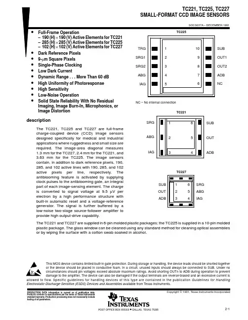
The TC221, TC225 and TC227 are full-framecharge-coupled device (CCD) image sensorsdesigned specifically for medical and industrialapplications where ruggedness and small size arerequired. The image-area diagonal measures1.3mm for the TC227, 2.4 mm for the TC221, and3.63 mm for the TC225. The image sensorscontain, in addition to dark reference pixels, 190,285, and 102 active lines with 190, 285, and 102active pixels per line, respectively. Theantiblooming feature is activated by supplyingclock pulses to the antiblooming gate, an integralpart of each image-sensing element. The chargeis converted to signal voltage at 9.5 µV perelectron by a high performance structure withbuilt-in automatic reset and a voltage-referencegenerator. The signal is further buffered by alow-noise two-stage source-follower amplifier toprovide high output-drive capability.
The TC221 and TC227 are supplied in 6-pin molded plastic packages; the TC225 is supplied in a 10-pin moldedplastic package. The glass window can be cleaned using any standard method for cleaning optical assembliesor by wiping the surface with a cotton swab soaked in alcohol.
This MOS device contains limited built-in gate protection. During storage or handling, the device leads should be shorted togetheror the device should be placed in conductive foam. In a circuit, unused inputs should always be connected to SUB. Under nocircumstances should pin voltages exceed absolute maximum ratings. Avoid shorting OUTn to ADB during operation to preventdamage to the amplifier. The device can also be damaged if the output terminals are reverse-biased and an excessive current isallowed to flow. Specific guidelines for handling devices of this type are contained in the publication Guidelines for HandlingElectrostatic-Discharge-Sensitive (ESDS) Devices and Assemblies available from Texas Instruments.TC225
TC221
TC22710
9
8
7
61
2
3
4
5
1
2
36
5
4
SUB
OUT
ADBSRG
ABG
IAGTRG
SRG1
SRG2
ABG
IAGSUB
OUT1
OUT2
ADB
NC
SRG
ABG
IAGSUB
OUT
ADB
1
2
36
5
4NC – No internal connection
PRODUCTION DATA information is current as of publication date.Products conform to specifications per the terms of Texas Instrumentsstandard warranty. Production processing does not necessarily includetesting of all parameters.
Dump Drain217 Pixels
911900.5OpticalBlack1ADB
OUT
SUB190Pixels
190LinesABG
IAG
SRGTop Drain
TC221
Dump DrainADB
OUT2
SUB285Pixels
285LinesABG
IAG
SRG2Top Drain
TC225SRG1OUT1TRG
1711142.51.5
1711.5142.51DummyElements
DummyElements15.5OpticalBlackTC221, TC225, TC227
SMALL-FORMAT CCD IMAGE SENSORS
SOCS037A – DECEMBER 1991
2-2POST OFFICE BOX 655303 • DALLAS, TEXAS 75265functional block diagrams
TC221, TC225, TC227
SMALL-FORMAT CCD IMAGE SENSORS
SOCS037A – DECEMBER 1991
2-3POST OFFICE BOX 655303 • DALLAS, TEXAS 75265functional block diagram
Dump Drain
129 Pixels
8116.51020.5
1VCC
VO
SUBABG
IAG
SRGTop Drain
TC227DummyElements102Lines102Pixels
TC221, TC225, TC227
SMALL-FORMAT CCD IMAGE SENSORS
SOCS037A – DECEMBER 1991
2-4POST OFFICE BOX 655303 • DALLAS, TEXAS 75265detailed description
The TC221, TC225, and TC227 consist of four basic functional blocks: (1) the image-sensing area, (2) the serialregisters, (3) the sensor node, and (4)the low-noise source-follower amplifier. The location of each of theseblocks is identified in the functional block diagram.
image-sensing area
As light enters the silicon in the image-sensing area, free electrons are generated and collected in the potentialwells of the sensing elements. During this time, blooming protection is activated by applying a burst of pulsesto the antiblooming gate. This prevents blooming by the spilling of charge from overexposed elements intoneighboring elements. After integration and under dark conditions, the charge is transferred line by line into theserial register(s). The required timing is shown in Figure 1 through Figure 3. During transfer, the antibloominggate is held at a low level. Each imager contains a specified number of dark pixels on the left side of theimage-sensing area. These elements provide the dark reference used in subsequent video-processing circuitsto restore the video black level.