上海交通大学李立利chapter 6. Structures for Discrete-Time Systems
- 格式:ppt
- 大小:144.50 KB
- 文档页数:12

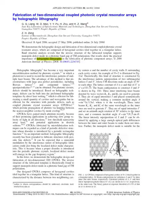
Fabrication of two-dimensional coupled photonic crystal resonator arrays by holographic lithographyG.Q.Liang,W.D.Mao,Y .Y .Pu,H.Zou,and H.Z.Wang a ͒State Key Laboratory of Optoelectronic Materials and Technologies,Zhongshan (Sun Yat-sen)University,Guangzhou 510275,People’s Republic of ChinaZ.H.ZengInstitute of Macromolecule,Zhongshan (Sun Yat-sen)University,Guangzhou 510275,People’s Republic of China͑Received 18April 2006;accepted 27May 2006;published online 24July 2006͒We demonstrate the holographic design and fabrication of two-dimensional coupled photonic crystal resonator arrays,which are composed of hexagonal cavities tiled together in a triangular lattice.Band structure analysis reveals that the inverse structure of the fabricated template supports monopole defect mode in a photonic band gap of TM polarization.Our results show the practical importance of holographic lithography in the fabrication of photonic component arrays.©2006American Institute of Physics .͓DOI:10.1063/1.2234743͔Holographic lithography 1has become a very important microfabrication method for photonic crystals,2,3in which a photoresist is used to record the interference patterns of mul-tiple laser beams.The advantage of this method is that mi-crostructures with large area perfect periodicities,includingBravais lattices 4–7and compound lattices,8–10quasiperiodicities 11–13can be obtained.For photonic circuits,defects should be introduced.Based on holographic tech-nique,defects can be built into the preformed holographic templates by direct laser writing,14which is efficient for fab-ricating a small quantity of cavities and waveguides but in-efficient for the structures with periodic defects,such as coupled photonic crystal resonator arrays ͑CPCRAs ͒,15which provide propagation of photons via hopping between the nearest-neighbor cavities by mode overlap.16,17CPCRAs have gained much attention recently,because of their promising applications in achieving slow group ve-locity of light in all directions,18low threshold nanocavity array laser,19and potential application in discrete solitons.20,21CPCRAs fabricated by microfabricaiton tech-niques can be regarded as a kind of periodic defective struc-ture whose disorder is introduced by a periodic rectangular function.15As an important method,holographic lithography recently has been extended to fabricate structures with peri-odic line defects.22It can be expected that a sinusoidal modulation by the interference nature of holographic fabri-cation could also bring the localized defect mode character-istic.This is because when a proper disorder is introduced into the periodic photonic crystals,localized defect modes will emerge in the gap frequency region.3In this letter,we demonstrate the holographic design and fabrication of two-dimensional ͑2D ͒CPCRA.The inverse structure of the fabricated template is theoretically found to support monopole defect mode in a photonic band gap of TM polarization.Our designed CPCRA composes of hexagonal cavities tiled together in a triangular lattice.This kind of structure is characterized by the distance between two neighboring cav-ity centers a and the number of cavity walls N surrounding each cavity center.An example of N =2is illustrated in Fig.1͑a ͒.Theoretically,this kind of structure is constructed by the interference pattern superposition of two subtriangular lattices S and S Ј,whose ⌫M directions make an angle of 30°to each other.The lattice constant of S is a and that of S Јis a Ј=a /͑N ͱ3͒.The beam configuration to construct S and S Јis shown in Fig.1͑b ͒.Three inner interfering laser beams denoted by wave vectors k 1,k 2,and k 3are used to generate S .They are of equal intensities I and placed symmetrically around the vertical,making a common incident angle =sin −1͑/1.5a ͒,where is the wavelength.Three outer beams k 1Ј,k 2Ј,and k 3Јof the same wavelength as the inner ones are used to generate S Ј.They are of equal intensities I Јand set an azimuth angle rotation of 30°relative to the inner ones,and a common incident angle Ј=sin −1͑N ͱ3sin ͒.The linear intensity superposition of S and S Јcan be ob-tained by applying a large enough optical path differences between the inner and outer beams to make them not inter-fere.Further,the monopole defect mode is suitable for thea ͒Author to whom correspondence should be addressed;electronic mail:stswhz@FIG.1.͑a ͒CPCRA composed of hexagonal cavities of N =2tiled together in a triangular lattice.͑b ͒Beam configurations for sublattices S and S Јby three inner and outer beams,respectively.Calculated patterns of S ,S Јand their linear superposed pattern when I /I Ј=0.2are shown in ͑c ͒–͑e ͒,respectively,at the same scale.The binary pattern at exposure threshold of 0.353of that in ͑e ͒is shown in ͑a ͒.APPLIED PHYSICS LETTERS 89,041902͑2006͒0003-6951/2006/89͑4͒/041902/3/$23.00©2006American Institute of Physics 89,041902-1Downloaded 17 May 2010 to 202.116.81.168. Redistribution subject to AIP license or copyright; see /apl/copyright.jsp2D CPCRAs,by which photons can couple to the nearest six neighboring cavities symmetrically.This mode can be gen-erated in a hexagonal cavity whose defect rod is of a smaller radius than those composing the cavity walls;23so primarily we choose the holographic patterns of S and S Јas circular rods and honeycomb structure,respectively,in the bright in-terference fields for superposition,which can be obtained by proper linear polarization combinations of the interfering beams.24Also,the symmetry of the cavity is determined by the relative position of S and S Ј,which depends on the pri-mary phases of two inner or two outer beams.25In principle,the phases can be adjusted by adding delay optics in the paths of the beams.What is more important,the relative intensity of the inner and outer beams I /I Јand the exposure threshold of the superposed pattern should be properly cho-sen for introducing appropriate disorder to S Јby S ,and even-tually constructing monopole defect modes localized in the cavities.To illustrate the above idea,an example of N =2is given here.We used =8°and Ј=29°.The polarization directions of the inner beams projected to the XOY plane making angles with OX are 1=83°,2=97°,and 3=270°,respectively,resulting the holographic pattern of S ,as shown in Fig.1͑c ͒.For the outer beams,1Ј=34°,2Ј=90°,and 3Ј=146°,result-ing S Ј,as shown in Fig.1͑d ͒.The theoretical superposition result is shown in Fig.1͑e ͒,where I /I Ј=0.2.The example in Fig.1͑a ͒is the binary pattern at exposure threshold 0.353of that in Fig.1͑e ͒.Here,exposure threshold is expressed as the percentage of the intensity range of the superposed patten.To decide the adoptable value of I /I Ј,band diagrams of the inverse structure of the superposed patterns formed by dif-ferent I /I Јand exposure threshold have been calculated with a refractive index ratio of 3.6by MIT PHOTONIC BANDS package.26The unit cell and high-symmetry points are shown in Fig.1͑a ͒.Results in the inset of Fig.2show that I /I Јshould be less than 1.1so that only a monopole defect mode can appear in a band gap of TM polarization.The exposure threshold range is fairly large when I /I Ј=0.2,of which the correspongding band gap edges and defect mode frequency ranges are also shown in Fig.2.In experiment,we used the 514.5nm line from an argon laser to obtain the six beams by beam splitters.All the inner beams were arranged to have the same optical path to createS ,so as for all the outer beams to create S Ј.For the sublattice superposition,the optical path difference between the inner and outer beams was being enlarged until the interference fringes between every inner and outer beams faded away,which was monitered by a charge-coupled device ͑CCD ͒camera.The relative positions of S and S Јwere also simul-taneously monitored,and the fabrication only needs single wavelength laser ouput and one-step exposure.The beams with longer time delay are collimated with a telescope sys-tem,which makes all the beams have the same diameters ϳ3mm.According to the above theoretical result,we used I =2mW and I Ј=10mW.To record the holographic pattern for a microstructure template,we used the photoresist made of the raw polymer resin Epon-SU8͑from Shell ͒dissolved in ␥-butyrolactone ͑1:1͒with cationic photoinitiator Irgacure 261͑2wt %͒.The photoresist solution was spin coated on glass plates and heated to ϳ83°C to remove any solvent before exposure.The optimal exposure time was ϳ3s.After the exposure,a postbake at ϳ93°C for 1.5h was used to complete the cross-linking of the resin.Polymerization occurred at regions where dosage of exposure from the superposed pattern ex-ceeded a critical value,while underexposed regions were washed away first by developing the sample in propylene-glycolmethyl-ether-acetate for 2h and then cleaned with ac-etone for 15min.Scanning electron microscope ͑SEM ͒images in Fig.3confirm the feasibility of such an experiment.A low magni-fication view illustrates the large area honeycomblike struc-ture of the sample,which is composed of hexagonal cavities tiled together in a triangular lattice.A closeup of the white rectangular zone is shown in the inset.These results indicate that the wave vector differences between the inner and outer beams do not give a periodic modulation to the superposed holographic pattern,since each inner beam cannot interfere with each outer beam,i.e.,we have obtained linear intensity superposition of two sublattices by applying large enough optical path difference between the inner and outer beams.ItFIG.2.Exposure threshold ranges of the superposed patterns as a function of I /I Ј͑inset ͒,within which can only a monopole defect mode emerge in a band gap of TM polorization from the inverse structures with refractive index ratio of 3.6.When I /I Ј=0.2,the band gap edges ͑dash lines ͒and defect mode frequency ranges ͑dark area ͒are alsoshown.FIG.3.SEM images of the fabricated CPCRA templates,showing large area honeycomblike structure of the sample,which is composed of hexago-nal cavities tiled together in a triangular lattice.A closeup of the white rectangular zone is shown in the inset.Four types of air holes are marked with “A,”“B,”“C,”and “D.”Downloaded 17 May 2010 to 202.116.81.168. Redistribution subject to AIP license or copyright; see /apl/copyright.jspwas found that four types of air holes,marked by “A,”“B,”“C,”and “D”in the inset of Fig.3,have deformation of different degrees compared to those in Fig.1͑a ͒.The most severe deformation happens to the C holes at the borderlines of two neighboring cavites.This is due to the more exposure dosage,consequently the more quantities of polymerization and shrinkage of the photoresist in the ⌫K directions than the ⌫M directions.It can be also seen that our samples are not quite uniform,which is due to alignment inaccuracies when setting the geometry configurations as well as angles among the interfering beams in experiment.Also because of the nonuniformity of the laser beams,there are regions where the phases do not favor the formation of the hexagonal cavities.While this work is a “proof-of-principle”experiment to dem-onstrate the creation of CPCRAs using sublattice superposi-tion,it is conceivable that better beam quality and control of beam phases can give large area uniform samples consisting of cavities like that shown in the inset middle of Fig.3.So theoretically we can use the middle cavity in the inset of Fig.3to construct the inverse structure for CPCRAs.The parameters are as follows:A holes and D holes become cir-cular dielectric rods with diameters 0.062a and 0.232a ,re-spectively.B holes and C holes become elliptical dielectric rods,with major and minor axes ͑0.142a ,0.129a ͒and ͑0.240a ,0.155a ͒,respectively.The calculated band diagram with refractive index ratio of 3.6for TM polarization is shown in Fig.4.It is found that a defect state exists within the second band gap.The eigenmode of this state is a mono-pole mode with enhanced electric field localized around the center of the unit cell,which serves as a resonant mode of the hexagonal cavities.A representative electric field inten-sity distribution of this mode at K point is shown in the inset.This result shows that 2D CPCRA templates can be fabri-cated by our holographic method.In conclusion,we have demonstrated the holographic de-sign and fabrication of two-dimensional coupled photonic crystal resonator arrays,which is composed of hexagonal cavities tiled together in a triangular lattice.The holographic pattern for this kind of structure was formed by linear inter-ference field superposition of sublattices.The inverse struc-ture of the fabricated template was proved to possess a monopole defect mode by band structure analysis.Our re-sults reveal that holographic lithography can be applied to the fabrication of photonic component arrays.This work is supported by the National Key Basic Re-search and Development of China under Grant No.2004CB719804,the National Natural Science Foundation of China.1K.Busch,S.Lölkes,R.B.Wehrspohn,and H.Föll,Photonic Crystals ͑Wiley,Weinheim,2004͒.2E.Yablonovitch,Phys.Rev.Lett.58,2059͑1987͒.3S.John,Phys.Rev.Lett.58,2486͑1987͒.4V .Berger,O.Gauthier-Lafaye,and E.Costard,J.Appl.Phys.82,60͑1997͒.5M.Campbell,D.N.Sharp,M.T.Harrison,R.G.Denning,and A.J.Turberfield,Nature ͑London ͒404,53͑2000͒.6X.Wang,J.F.Xu,H.M.Su,Z.H.Zeng,Y .L.Chen,H.Z.Wang,Y .K.Pang,and W.Y .Tam,Appl.Phys.Lett.82,2212͑2003͒.7Y .C.Zhong,S.A.Zhu,H.M.Su,H.Z.Wang,J.M.Chen,Z.H.Zeng,and Y .L.Chen,Appl.Phys.Lett.87,061103͑2005͒.8W.D.Mao,J.W.Dong,Y .C.Zhong,G.Q.Liang,and H.Z.Wang,Opt.Express 13,2994͑2005͒.9L.Wu,Y .C.Zhong,K.S.Wong,G.P.Wang,and L.Yuan,Appl.Phys.Lett.88,091115͑2006͒.10W.D.Mao,G.Q.Liang,H.Zou,and H.Z.Wang,Opt.Lett.31,1708͑2006͒.11X.Wang,C.Y .Ng,W.Y .Tam,C.T.Chan,and P.Sheng,Adv.Mater.͑Weinheim,Ger.͒15,1526͑2003͒.12X.Wang,J.Xu,J.C.W.Lee,Y .K.Pang,W.Y .Tam,C.T.Chan,and P.Sheng,Appl.Phys.Lett.88,051901͑2006͒.13S.P.Gorkhali,J.Qi,and G.P.Crawford,J.Opt.Soc.Am.B 23,149͑2006͒.14H.B.Sun,A.Nakamura,K.Kaneko,and S.Shoji,Opt.Lett.30,881͑2005͒.15H.Altug and J.Vu čkovi ć,Appl.Phys.Lett.84,161͑2004͒.16M.Bayindir,B.Temelkuran,and E.Ozbay,Phys.Rev.Lett.84,2140͑2000͒.17M.Bayindir,B.Temelkuran,and E.Ozbay,Phys.Rev.B 61,R11855͑2000͒.18H.Altug and J.Vu čkovi ć,Appl.Phys.Lett.86,111102͑2005͒.19H.Altug and J.Vu čkovi ć,Opt.Express 13,8819͑2005͒.20D.N.Christodoulides and N.K.Efremidis,Opt.Lett.27,568͑2002͒.21J.W.Fleischer,M.Segev,N.K.Efremidis,and D.N.Christodoulides,Nature ͑London ͒422,147͑2003͒.22C.Chang,T.M.Yan,and H.K.Liu,Appl.Opt.44,2580͑2005͒.23K.Sakoda,J.Appl.Phys.84,1210͑1998͒.24H.M.Su,Y .C.Zhong,X.Wang,X.G.Zheng,J.F.Xu,and H.Z.Wang,Phys.Rev.E 67,056619͑2003͒.25Y .C.Zhong,S.A.Zhu,and H.Z.Wang,Chin.Phys.Lett.22,369͑2005͒.26S.G.Johnson and J.D.Joannopoulos,Opt.Express 8,173͑2001͒.FIG.4.Band diagram of a CPCRA constructed by the inverse structure of the middle cavity in the inset of Fig.3with refractive index ratio of 3.6.A monopole defect mode ͑dot line with open circles ͒emerges in the second band gap for TM polarization.The electric field intensity distribution of this mode at K point is shown in the inset.Downloaded 17 May 2010 to 202.116.81.168. Redistribution subject to AIP license or copyright; see /apl/copyright.jsp。