MM5Z47VT1G稳压二极管规格书
- 格式:pdf
- 大小:312.15 KB
- 文档页数:4
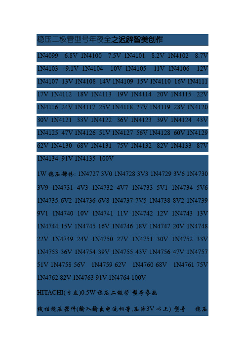
稳压二极管型号年夜全之迟辟智美创作1N4099 6.8V 1N4100 7.5V 1N4101 8.2V 1N4102 8.7V 1N4103 9.1V 1N4104 10V 1N4105 11V 1N4106 12V 1N4107 13V 1N4108 14V 1N4109 15V 1N4110 16V 1N4111 17V 1N4112 18V 1N4113 19V 1N4114 20V 1N4115 22V 1N4116 24V 1N4117 25V 1N4118 27V 1N4119 28V 1N4120 30V 1N4121 33V 1N4122 36V 1N4123 39V 1N4124 43V 1N4125 47V 1N4126 51V 1N4127 56V 1N4128 60V 1N4129 62V 1N4130 68V 1N4131 75V 1N4132 82V 1N4133 87V 1N4134 91V 1N4135 100V1W稳压部份: 1N4727 3V0 1N4728 3V3 1N4729 3V6 1N4730 3V9 1N4731 4V3 1N4732 4V7 1N4733 5V1 1N4734 5V6 1N4735 6V2 1N4736 6V8 1N4737 7V5 1N4738 8V2 1N4739 9V1 1N4740 10V 1N4741 11V 1N4742 12V 1N4743 13V 1N4744 15V 1N4745 16V 1N4746 18V 1N4747 20V 1N4748 22V 1N4749 24V 1N4750 27V 1N4751 30V 1N4752 33V 1N4753 36V 1N4754 39V 1N4755 43V 1N4756 47V 1N4757 51V 1N4758 56V 1N4759 62V 1N4760 68V 1N4761 75V 1N4762 82V 1N4763 91V 1N4764 100VHITACHI(日立)0.5W稳压二极管型号参数线性稳压器件(输入输出电流相等,压降3V以上) 型号稳压(V) 最年夜输出电流可替代型号79L05 -5V 100mA79L06 -6V 100mA 79L08 -8V 100mA LM7805 5V1A L7805,LM340T5 LM7806 6V 1A L7806LM7808 8V 1A L7808 LM7809 9V 1A L7809 LM7812 12V 1A L7812,LM340T12LM7815 15V 1A L7815,LM340T15 LM7818 18V1A L7815 LM7824 24V 1A L7824 LM7905-5V 1A L7905 LM7906 -6V 1A L7906,KA7906 LM7908 -8V 1A L7908 LM7909 -9V 1A L7909 LM7912 -12V 1A L7912LM7915 -15V 1A L7915 LM7918 -18V 1A L7918 LM7924 -24V 1A L7924 78L05 5V 100mA 78L06 6V 100mA 78L08 8V 100ma78L09 9V 100ma 78L12 12V 100ma 78L15 15V 100ma 78L18 18V 100ma 78L24 24V 100ma开关稳压器件(电压转换效率高) 型号说明最年夜输出电流LM1575T-3.3 3.3V简易开关电源稳压器1A LM1575T-5.0 5V简易开关电源稳压器 1A LM1575T-12 12V简易开关电源稳压器1A LM1575T-15 15V简易开关电源稳压器1A LM1575T-ADJ 简易开关电源稳压器(可调1.23V~37V) 1ALM1575HVT-3.3 3.3V简易开关电源稳压器1ALM1575HVT-5.0 5V简易开关电源稳压器1A LM1575HVT-12 12V简易开关电源稳压器1A LM1575HVT-15 15V简易开关电源稳压器1A LM1575HVT-ADJ 简易开关电源稳压器(可调1.23V~37V) 1A LM2575T-3.3 3.3V简易开关电源稳压器 1A LM2575T-5.0 5V简易开关电源稳压器1A LM2575T-12 12V简易开关电源稳压器1A LM2575T-15 15V简易开关电源稳压器1A LM2575T-ADJ 简易开关电源稳压器(可调1.23V~ 37V) 1A LM2575HVT-3.3 3.3V简易开关电源稳压器1A LM2575HVT-5.0 5V简易开关电源稳压器1A LM2575HVT-12 12V简易开关电源稳压器1A LM2575HVT-15 15V简易开关电源稳压器1A LM2575HVT-ADJ 简易开关电源稳压器(可调1.23V~37V) 1A LM2576T-3.3 3.3V简易开关电源稳压器 3A LM2576T-5.0 5.0V简易开关电源稳压器3A LM2576T-12 12V简易开关电源稳压器3A LM2576T-15 15V简易开关电源稳压器3A LM2576T-ADJ 简易开关电源稳压器(可调1.23V~37V) 3A LM2576HVT-3.3 3.3V简易开关电源稳压器3A LM2576HVT-5.0 5.0V简易开关电源稳压器3A LM2576HVT-12 12V简易开关电源稳压器3ALM2576HVT-15 15V简易开关电源稳压器3A LM2576HVT-ADJ 简易开关电源稳压器(可调1.23V~37V) 3A。
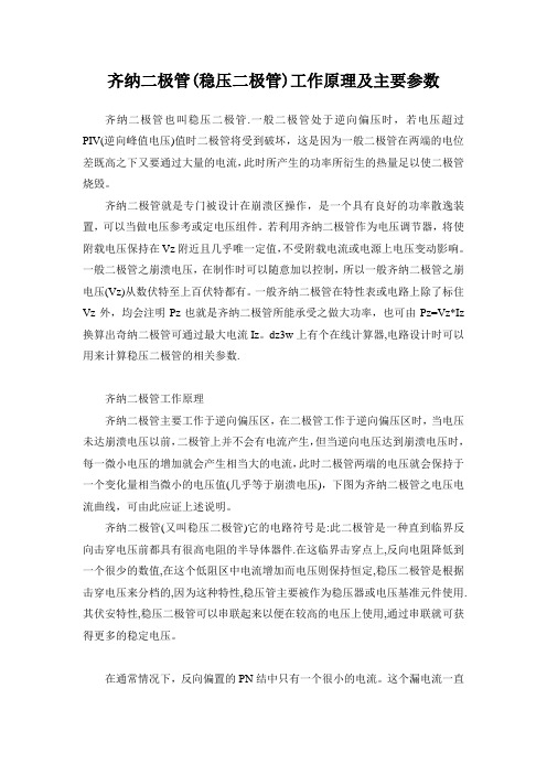
齐纳二极管(稳压二极管)工作原理及主要参数齐纳二极管也叫稳压二极管.一般二极管处于逆向偏压时,若电压超过PIV(逆向峰值电压)值时二极管将受到破坏,这是因为一般二极管在两端的电位差既高之下又要通过大量的电流,此时所产生的功率所衍生的热量足以使二极管烧毁。
齐纳二极管就是专门被设计在崩溃区操作,是一个具有良好的功率散逸装置,可以当做电压参考或定电压组件。
若利用齐纳二极管作为电压调节器,将使附载电压保持在Vz附近且几乎唯一定值,不受附载电流或电源上电压变动影响。
一般二极管之崩溃电压,在制作时可以随意加以控制,所以一般齐纳二极管之崩电压(Vz)从数伏特至上百伏特都有。
一般齐纳二极管在特性表或电路上除了标住Vz外,均会注明Pz也就是齐纳二极管所能承受之做大功率,也可由Pz=Vz*Iz 换算出奇纳二极管可通过最大电流Iz。
dz3w上有个在线计算器,电路设计时可以用来计算稳压二极管的相关参数.齐纳二极管工作原理齐纳二极管主要工作于逆向偏压区,在二极管工作于逆向偏压区时,当电压未达崩溃电压以前,二极管上并不会有电流产生,但当逆向电压达到崩溃电压时,每一微小电压的增加就会产生相当大的电流,此时二极管两端的电压就会保持于一个变化量相当微小的电压值(几乎等于崩溃电压),下图为齐纳二极管之电压电流曲线,可由此应证上述说明。
齐纳二极管(又叫稳压二极管)它的电路符号是:此二极管是一种直到临界反向击穿电压前都具有很高电阻的半导体器件.在这临界击穿点上,反向电阻降低到一个很少的数值,在这个低阻区中电流增加而电压则保持恒定,稳压二极管是根据击穿电压来分档的,因为这种特性,稳压管主要被作为稳压器或电压基准元件使用.其伏安特性,稳压二极管可以串联起来以便在较高的电压上使用,通过串联就可获得更多的稳定电压。
在通常情况下,反向偏置的PN结中只有一个很小的电流。
这个漏电流一直保持一个常数,直到反向电压超过某个特定的值,超过这个值之后PN结突然开始有大电流导通(图1.15)。

Zener Voltage Regulators150mW SOD–523Surface MountWe declare that the material of product compliance with RoHS requirements.ORDERING INFORMATIONDevice Package Shipping MM5ZXXXT1GSOD-5233000/Tape&ReelThis series of Zener diodes is packaged in a SOD–523surface mount package that has a power dissipation of 100mW.They are designed to provide voltage regulation protection and are especially attractive in situations where space is at a premium.They are well suited for applications such as cellular phones,hand held portables,and high density PC boards.Specification Features:•Standard Zener Breakdown Voltage Range –2.4V to 75V •Steady State Power Rating of 200mW•Small Body Outline Dimensions:0.047"x 0.032"(1.20mm x 0.80mm)•Low Body Height:0.028"(0.7mm)•ESD Rating of Class 3(>16kV)per Human Body ModelMechanical Characteristics:CASE:Void-free,transfer-molded,thermosetting plastic Epoxy Meets UL 94V-0LEAD FINISH:100%Matte Sn (Tin)QUALIFIED MAX REFLOW TEMPERATURE:260°C Device Meets MSL 1Requirements MOUNTING POSITION:AnyMAXIMUM RATINGSRatingSymbol Max Unit Total Device Dissipation FR−5Board,P D150mW@T A =25︒C Junction and Storage T J,Tstg−65to ︒CTemperature Range+150Maximum ratings are those values beyond which devicedamage can occur.Maximum ratings applied to the device are individual stress limit values (not normal operating conditions)and are not valid simultaneously.If these limits are exceeded,device functional operation is not implied,damage may occur and reliability may be affected.MM5Z2V4T1G SERIES12CATHODE ANODEMARKING DIAGRAMxx dxx=Specific Device Code d =Date CodeSOD–523MM5Z2V4T1G SERIES ELECTRICAL CHARACTERISTICS I(T A=25︒C unless otherwise noted,I FV F=0.9V Max.@I F=10mA for all types)Symbol ParameterVZ Reverse Zener Voltage@I ZT IZT Reverse Current VZVRVZ ZT Maximum Zener Impedance@I I R VFZT IZTIZK Reverse CurrentZZK Maximum Zener Impedance@I ZKIR Reverse Leakage Current@V RV R Reverse VoltageI F Forward Current Zener Voltage Regulator V F Forward Voltage@I FQV Z Maximum Temperature Coefficient of V ZC Max.Capacitance@V R=0and f=1MHz100(%)80DISS IP ATI ON 60 40POWER20255075100125150TEMPERATURE(︒C)Figure1.Steady State Power Derating MM5Z2V4T1G SERIESELECTRICAL CHARACTERISTICS (T A =25︒C unless otherwise noted,V F =0.9V Max.@I F =10mA for all types)Zener Voltage (Note 1)Zener Impedance Leakage CurrentQ V Z C ZZT(mV/k)@V =0V(Volts)@I@I ZT Z@II @VRZZKR@IZTf =1MHzDevice ZTZKRDevice Marking Min Nom Max mA W W mA m A Volts Min Max pF MM5Z2V4T1G 00 2.2 2.4 2.651001000 1.050 1.0−3.50450MM5Z2V7T1G 01 2.5 2.7 2.951001000 1.020 1.0−3.50450MM5Z3V0T1G 02 2.8 3.0 3.251001000 1.010 1.0−3.50450MM5Z3V3T1G 05 3.1 3.3 3.55951000 1.05 1.0−3.50450MM5Z3V6T1G 06 3.4 3.6 3.85901000 1.05 1.0−3.50450MM5Z3V9T1G 07 3.7 3.9 4.15901000 1.03 1.0−3.5−2.5450MM5Z4V3T1G 08 4.0 4.3 4.65901000 1.03 1.0−3.50450MM5Z4V7T1G 09 4.4 4.7 5.0580800 1.03 2.0−3.50.2260MM5Z5V1T1G 0A 4.8 5.1 5.4560500 1.02 2.0−2.7 1.2225MM5Z5V6T1G 0C 5.2 5.6 6.0540400 1.01 2.0−2.0 2.5200MM5Z6V2T1G 0E 5.8 6.2 6.6510100 1.03 4.00.4 3.7185MM5Z6V8T1G 0F 6.4 6.87.2515160 1.02 4.0 1.2 4.5155MM5Z7V5T1G 0G 7.07.57.9515160 1.01 5.0 2.5 5.3140MM5Z8V2T1G 0H 7.78.28.7515160 1.00.7 5.0 3.2 6.2135MM5Z9V1T1G 0K 8.59.19.6515160 1.00.27.0 3.87.0130MM5Z10VT1G 0L 9.41010.6520160 1.00.18.0 4.58.0130MM5Z11VT1G 0M 10.41111.6520160 1.00.18.0 5.49.0130MM5Z12VT1G 0N 11.41212.752580 1.00.18.0 6.010130MM5Z13VT1G 0P 12.413.2514.153080 1.00.18.07.011120MM5Z15VT1G 0T 14.31515.8530200 1.00.0510.59.213110MM5Z16VT1G 0U 15.316.217.1240200 1.00.0511.210.414105MM5Z18VT1G 0W 16.81819.1245225 1.00.0512.612.416100MM5Z20VT1G 0Z 18.82021.2255225 1.00.0514.014.41885MM5Z22VT1G 1020.82223.3255250 1.00.0515.416.42085MM5Z24VT1G 1122.824.225.6270120 1.00.0516.818.42280MM5Z27VT1G 1225.12728.9280300 1.00.0518.921.425.370MM5Z30VT1G 14283032280300 1.00.0521.024.429.470MM5Z33VT1G 18313335280300 1.00.0523.227.433.470MM5Z36VT1G 19343638290500 1.00.0525.230.437.470MM5Z39VT1G 203739412130500 1.00.0527.333.441.245MM5Z43VT1G 214043461150500 1.00.0530.137.646.640MM5Z47VT1G 1A 4447501170500 1.00.0532.942.051.840MM5Z51VT1G 1C 4851541180500 1.00.0535.746.657.240MM5Z56VT1G 1D 5256601200500 1.00.0539.252.263.840MM5Z62VT1G 1E 5862661215500 1.00.0543.458.871.635MM5Z68VT1G 1F 6468721240500 1.00.0547.665.679.835MM5Z75VT1G1G70757912555001.00.0552.573.488.6351.Zener voltage is measured with a pulse test current I Z at an ambient temperature of 25︒C.MM5Z2V4T1G SERIESSC-79/SOD-523DIMENSIONS (mm are the original dimensions)UNIT A b p c D E H E V m m0.70.350.2 1.30.9 1.70.150.50.250.11.10.71.5Note1.The marking bar indicates the cathode.OUTLINE REFERENCES EUROPEAN ISSUE DATEVERSION IECJEDECEIAJ PROJECTIONSOD523SC-7998-11-25。
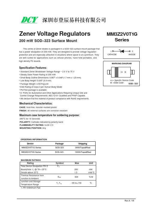
Zener Voltage Regulators200 mW SOD–323 Surface MountMM3Z2V0T1GSeriesThis series of Zener diodes is packaged in a SOD–323 surface mount package that has a power dissipation of 200 mW. They are designed to provide voltage regulation protection and are especially attractive in situations where space is at a premium. They are well suited for applications such as cellular phones, hand held portables, and high density PC boards.Specification Features:• Standard Zener Breakdown Voltage Range – 2.0 V to 75 V • Steady State Power Rating of 200 mW• Small Body Outline Dimensions: 0.067" x 0.049"(1.7 mm x 1.25 mm).Low Body Height: 0.035" (0.9 mm)• Package Weight: 4.507mg/unit• ESD Rating of Class 3 per Human Body Model • Pb-Free package is available.Mechanical Characteristics:CASE:Void-free, transfer-molded plasticFINISH:All external surfaces are corrosion resistant260°C for 10 SecondsPOLARITY:Cathode indicated by polarity band FLAMMABILITY RATING: UL94 V-0MOUNTING POSITION: AnyMAXIMUM RATINGSRating SymbolMax UnitTotal Device Dissipation FR–5 P DBoard(Note 1.) @ TA = 25°C 200 mW Derate above 25°C 1.5mW/°C Thermal Resistance fromR θJA635 °C/W Junction to Ambient Junction and StorageT J , T stg –65 to+150 °CTemperature Range 1. FR–4 Minimum PadDevicePackageShippingMM3Z2V0T1G Series SOD-3233000/Tape&ReelMM3Z2V0T3G SeriesSOD-32310000/Tape&ReelRev.A 1/6• S- Prefix for Automotive and Other Applications Requiring Unique Site and Control Change Requirements; AEC-Q101 Qualified and PPAP Capable.• We declare that the material of product compliance with RoHS requirements.ORDERING INFORMATIONMaximum case temperature for soldering purpose:MM3Z2V0T1G SeriesELECTRICAL CHARACTERISTICS(T A = 25°C unless otherwise noted,V F = 0.9 V Max. @ IF = 10 mA for all types)Symbol ParameterV Z Reverse Zener Voltage @ I ZT I ZT Reverse CurrentZ ZT Maximum Zener Impedance @ I ZT I ZK Reverse CurrentZ ZK Maximum Zener Impedance @ I ZK I R Reverse Leakage Current @ V R V R Reverse Voltage I F Forward Current V F Forward Voltage @ I FQ V Z Maximum Temperature Coefficient of V Z CMax. Capacitance @V R = 0 and f = 1 MHzRev.A 2/62.Zener voltage is measured with a pulse test current I Z at an ambient temperature of 25°C.Rev.A 3/6MM3Z2V0T1G SeriesTypical CharacteristicsZ Z T , D Y N A M I C I M P E D A N C E ()Ω1000100101.0C , C A P A C I T A N C E (p F )70V Z , NOMINAL ZENER VOLTAGE (V)Figure 3. Typical Capacitance 104.0V Z , NOMINAL ZENER VOLTAGE (V)Figure 4. Typical Leakage Current70605040302010Rev.A 4/6MM3Z2V0T1G SeriesTypical Characteristics12V Z , ZENER VOLTAGE (V)100101.00.10.01108.06.04.02.00I Z , Z E N E R C U R R E N T (m A )V Z , ZENER VOLTAGE (V)Figure 5. Zener Voltage versus Zener Current(V Z Up to 12 V)Figure 6. Zener Voltage versus Zener Current(12 V to 75 V)1001010.10.011030507090I Z , Z E N E R C U R R E N T (m A )Figure 7. Steady State Power DeratingRev.A 5/6300200100005025100150P O W E R D I S S I P A T I O N : P d (m W )AMBIENT TEMPERA TURE : T a (°C)MM3Z2V0T1G SeriesPACKAGE DIMENSIONSSOD-323Rev.A 6/6HE NOTES:1.DIMENSIONING AND TOLERANCING PER ANSI Y14.5M, 1982.2.CONTROLLING DIMENSION: MILLIMETERS.3.LEAD THICKNESS SPECIFIED PER L/F DRAWING WITH SOLDER PLATING.4.DIMENSIONS A AND B DO NOT INCLUDE MOLD FLASH, PROTRUSIONS OR GATE BURRS.5.DIMENSION L IS MEASURED FROM END OF RADIUS.NOTE 3DIM MIN NOM MAX MILLIMETERSA 0.800.90 1.00A10.000.050.10A30.15 REF b 0.250.320.4C 0.0890.120.177D 1.60 1.70 1.80E 1.15 1.25 1.350.082.30 2.50 2.70L 0.0310.0350.0400.0000.0020.0040.006 REF0.0100.0120.0160.0030.0050.0070.0620.0660.0700.0450.0490.0530.0030.0900.0980.105MINNOM MAX INCHESSOLDERING FOOTPRINT*MM3Z2V0T1G Series。
Zener Voltage Regulators150mW SOD–523Surface MountWe declare that the material of product compliance with RoHS requirements.ORDERING INFORMATIONDevice Package Shipping MM5ZXXXT1GSOD-5233000/Tape&ReelThis series of Zener diodes is packaged in a SOD–523surface mount package that has a power dissipation of 100mW.They are designed to provide voltage regulation protection and are especially attractive in situations where space is at a premium.They are well suited for applications such as cellular phones,hand held portables,and high density PC boards.Specification Features:•Standard Zener Breakdown Voltage Range –2.4V to 75V •Steady State Power Rating of 200mW•Small Body Outline Dimensions:0.047"x 0.032"(1.20mm x 0.80mm)•Low Body Height:0.028"(0.7mm)•ESD Rating of Class 3(>16kV)per Human Body ModelMechanical Characteristics:CASE:Void-free,transfer-molded,thermosetting plastic Epoxy Meets UL 94V-0LEAD FINISH:100%Matte Sn (Tin)QUALIFIED MAX REFLOW TEMPERATURE:260°C Device Meets MSL 1Requirements MOUNTING POSITION:AnyMAXIMUM RATINGSRatingSymbol Max Unit Total Device Dissipation FR−5Board,P D150mW@T A =25︒C Junction and Storage T J,Tstg−65to ︒CTemperature Range+150Maximum ratings are those values beyond which devicedamage can occur.Maximum ratings applied to the device are individual stress limit values (not normal operating conditions)and are not valid simultaneously.If these limits are exceeded,device functional operation is not implied,damage may occur and reliability may be affected.MM5Z2V4T1G SERIES12CATHODE ANODEMARKING DIAGRAMxx dxx=Specific Device Code d =Date CodeSOD–523MM5Z2V4T1G SERIES ELECTRICAL CHARACTERISTICS I(T A=25︒C unless otherwise noted,I FV F=0.9V Max.@I F=10mA for all types)Symbol ParameterVZ Reverse Zener Voltage@I ZT IZT Reverse Current VZVRVZ ZT Maximum Zener Impedance@I I R VFZT IZTIZK Reverse CurrentZZK Maximum Zener Impedance@I ZKIR Reverse Leakage Current@V RV R Reverse VoltageI F Forward Current Zener Voltage Regulator V F Forward Voltage@I FQV Z Maximum Temperature Coefficient of V ZC Max.Capacitance@V R=0and f=1MHz100(%)80DISS IP ATI ON 60 40POWER20255075100125150TEMPERATURE(︒C)Figure1.Steady State Power Derating MM5Z2V4T1G SERIESELECTRICAL CHARACTERISTICS (T A =25︒C unless otherwise noted,V F =0.9V Max.@I F =10mA for all types)Zener Voltage (Note 1)Zener Impedance Leakage CurrentQ V Z C ZZT(mV/k)@V =0V(Volts)@I@I ZT Z@II @VRZZKR@IZTf =1MHzDevice ZTZKRDevice Marking Min Nom Max mA W W mA m A Volts Min Max pF MM5Z2V4T1G 00 2.2 2.4 2.651001000 1.050 1.0−3.50450MM5Z2V7T1G 01 2.5 2.7 2.951001000 1.020 1.0−3.50450MM5Z3V0T1G 02 2.8 3.0 3.251001000 1.010 1.0−3.50450MM5Z3V3T1G 05 3.1 3.3 3.55951000 1.05 1.0−3.50450MM5Z3V6T1G 06 3.4 3.6 3.85901000 1.05 1.0−3.50450MM5Z3V9T1G 07 3.7 3.9 4.15901000 1.03 1.0−3.5−2.5450MM5Z4V3T1G 08 4.0 4.3 4.65901000 1.03 1.0−3.50450MM5Z4V7T1G 09 4.4 4.7 5.0580800 1.03 2.0−3.50.2260MM5Z5V1T1G 0A 4.8 5.1 5.4560500 1.02 2.0−2.7 1.2225MM5Z5V6T1G 0C 5.2 5.6 6.0540400 1.01 2.0−2.0 2.5200MM5Z6V2T1G 0E 5.8 6.2 6.6510100 1.03 4.00.4 3.7185MM5Z6V8T1G 0F 6.4 6.87.2515160 1.02 4.0 1.2 4.5155MM5Z7V5T1G 0G 7.07.57.9515160 1.01 5.0 2.5 5.3140MM5Z8V2T1G 0H 7.78.28.7515160 1.00.7 5.0 3.2 6.2135MM5Z9V1T1G 0K 8.59.19.6515160 1.00.27.0 3.87.0130MM5Z10VT1G 0L 9.41010.6520160 1.00.18.0 4.58.0130MM5Z11VT1G 0M 10.41111.6520160 1.00.18.0 5.49.0130MM5Z12VT1G 0N 11.41212.752580 1.00.18.0 6.010130MM5Z13VT1G 0P 12.413.2514.153080 1.00.18.07.011120MM5Z15VT1G 0T 14.31515.8530200 1.00.0510.59.213110MM5Z16VT1G 0U 15.316.217.1240200 1.00.0511.210.414105MM5Z18VT1G 0W 16.81819.1245225 1.00.0512.612.416100MM5Z20VT1G 0Z 18.82021.2255225 1.00.0514.014.41885MM5Z22VT1G 1020.82223.3255250 1.00.0515.416.42085MM5Z24VT1G 1122.824.225.6270120 1.00.0516.818.42280MM5Z27VT1G 1225.12728.9280300 1.00.0518.921.425.370MM5Z30VT1G 14283032280300 1.00.0521.024.429.470MM5Z33VT1G 18313335280300 1.00.0523.227.433.470MM5Z36VT1G 19343638290500 1.00.0525.230.437.470MM5Z39VT1G 203739412130500 1.00.0527.333.441.245MM5Z43VT1G 214043461150500 1.00.0530.137.646.640MM5Z47VT1G 1A 4447501170500 1.00.0532.942.051.840MM5Z51VT1G 1C 4851541180500 1.00.0535.746.657.240MM5Z56VT1G 1D 5256601200500 1.00.0539.252.263.840MM5Z62VT1G 1E 5862661215500 1.00.0543.458.871.635MM5Z68VT1G 1F 6468721240500 1.00.0547.665.679.835MM5Z75VT1G1G70757912555001.00.0552.573.488.6351.Zener voltage is measured with a pulse test current I Z at an ambient temperature of 25︒C.MM5Z2V4T1G SERIESSC-79/SOD-523DIMENSIONS (mm are the original dimensions)UNIT A b p c D E H E V m m0.70.350.2 1.30.9 1.70.150.50.250.11.10.71.5Note1.The marking bar indicates the cathode.OUTLINE REFERENCES EUROPEAN ISSUE DATEVERSION IECJEDECEIAJ PROJECTIONSOD523SC-7998-11-25。
稳压二极管规格啥是稳压二极管呢?稳压二极管就是一种能让电压保持稳定的小玩意儿。
它就像一个电压小卫士,守护着电路中的电压,不让它乱跳。
那稳压二极管的规格都有啥呢?首先得说说它的稳压值。
这就像是给稳压二极管定了一个目标电压。
比如说,有个稳压二极管的稳压值是 5 伏,那它的任务就是让电路中的电压尽量保持在 5 伏左右。
如果电压高了,它就会想办法把电压降下来;如果电压低了,它又会努力把电压升上去。
就像一个超级负责的小管家,时刻盯着电压,不让它出乱子。
然后呢,还有一个重要的规格是最大工作电流。
这就像是给稳压二极管规定了一个能承受的最大工作量。
如果电流超过了这个最大值,稳压二极管可能就会累垮,不能正常工作了。
所以在使用稳压二极管的时候,我们得注意不能让电流太大,不然它可就罢工啦。
还有反向击穿电压也很重要哦。
啥是反向击穿电压呢?简单来说,就是当给稳压二极管加一个反向电压,加到一定程度的时候,它就会被“击穿”,开始导通。
但是这个反向击穿可不是坏事儿哦,它正是稳压二极管能发挥作用的关键。
不过,如果反向电压超过了它的反向击穿电压,那稳压二极管可就真的被弄坏了。
所以我们得知道稳压二极管的反向击穿电压是多少,这样才能安全地使用它。
另外,稳压二极管的功率也是一个需要关注的规格。
功率就像是稳压二极管的“力气”大小。
如果一个稳压二极管的功率大,那它就能承受更大的电流和电压,也能更好地完成稳压的任务。
但是如果功率小,可能就只能用在一些小电流、小电压的场合。
那这些规格对我们有啥用呢?比如说,我们在做电子小制作的时候,如果需要一个稳定的 5 伏电压,那我们就可以找一个稳压值是 5 伏的稳压二极管。
然后再根据我们的电路需要,看看需要多大的工作电流和功率,选择合适的稳压二极管。
如果选错了,可能就会导致电路不能正常工作,或者稳压二极管被烧坏。
而且,不同的稳压二极管规格也会影响它的价格哦。
一般来说,稳压值高、功率大、工作电流大的稳压二极管会比较贵。
Zener Voltage Regulators150mW SOD–523Surface MountWe declare that the material of product compliance with RoHS requirements.ORDERING INFORMATIONDevice Package Shipping MM5ZXXXT1GSOD-5233000/Tape&ReelThis series of Zener diodes is packaged in a SOD–523surface mount package that has a power dissipation of 100mW.They are designed to provide voltage regulation protection and are especially attractive in situations where space is at a premium.They are well suited for applications such as cellular phones,hand held portables,and high density PC boards.Specification Features:•Standard Zener Breakdown Voltage Range –2.4V to 75V •Steady State Power Rating of 200mW•Small Body Outline Dimensions:0.047"x 0.032"(1.20mm x 0.80mm)•Low Body Height:0.028"(0.7mm)•ESD Rating of Class 3(>16kV)per Human Body ModelMechanical Characteristics:CASE:Void-free,transfer-molded,thermosetting plastic Epoxy Meets UL 94V-0LEAD FINISH:100%Matte Sn (Tin)QUALIFIED MAX REFLOW TEMPERATURE:260°C Device Meets MSL 1Requirements MOUNTING POSITION:AnyMAXIMUM RATINGSRatingSymbol Max Unit Total Device Dissipation FR−5Board,P D150mW@T A =25︒C Junction and Storage T J,Tstg−65to ︒CTemperature Range+150Maximum ratings are those values beyond which devicedamage can occur.Maximum ratings applied to the device are individual stress limit values (not normal operating conditions)and are not valid simultaneously.If these limits are exceeded,device functional operation is not implied,damage may occur and reliability may be affected.MM5Z2V4T1G SERIES12CATHODE ANODEMARKING DIAGRAMxx dxx=Specific Device Code d =Date CodeSOD–523MM5Z2V4T1G SERIES ELECTRICAL CHARACTERISTICS I(T A=25︒C unless otherwise noted,I FV F=0.9V Max.@I F=10mA for all types)Symbol ParameterVZ Reverse Zener Voltage@I ZT IZT Reverse Current VZVRVZ ZT Maximum Zener Impedance@I I R VFZT IZTIZK Reverse CurrentZZK Maximum Zener Impedance@I ZKIR Reverse Leakage Current@V RV R Reverse VoltageI F Forward Current Zener Voltage Regulator V F Forward Voltage@I FQV Z Maximum Temperature Coefficient of V ZC Max.Capacitance@V R=0and f=1MHz100(%)80DISS IP ATI ON 60 40POWER20255075100125150TEMPERATURE(︒C)Figure1.Steady State Power Derating MM5Z2V4T1G SERIESELECTRICAL CHARACTERISTICS (T A =25︒C unless otherwise noted,V F =0.9V Max.@I F =10mA for all types)Zener Voltage (Note 1)Zener Impedance Leakage CurrentQ V Z C ZZT(mV/k)@V =0V(Volts)@I@I ZT Z@II @VRZZKR@IZTf =1MHzDevice ZTZKRDevice Marking Min Nom Max mA W W mA m A Volts Min Max pF MM5Z2V4T1G 00 2.2 2.4 2.651001000 1.050 1.0−3.50450MM5Z2V7T1G 01 2.5 2.7 2.951001000 1.020 1.0−3.50450MM5Z3V0T1G 02 2.8 3.0 3.251001000 1.010 1.0−3.50450MM5Z3V3T1G 05 3.1 3.3 3.55951000 1.05 1.0−3.50450MM5Z3V6T1G 06 3.4 3.6 3.85901000 1.05 1.0−3.50450MM5Z3V9T1G 07 3.7 3.9 4.15901000 1.03 1.0−3.5−2.5450MM5Z4V3T1G 08 4.0 4.3 4.65901000 1.03 1.0−3.50450MM5Z4V7T1G 09 4.4 4.7 5.0580800 1.03 2.0−3.50.2260MM5Z5V1T1G 0A 4.8 5.1 5.4560500 1.02 2.0−2.7 1.2225MM5Z5V6T1G 0C 5.2 5.6 6.0540400 1.01 2.0−2.0 2.5200MM5Z6V2T1G 0E 5.8 6.2 6.6510100 1.03 4.00.4 3.7185MM5Z6V8T1G 0F 6.4 6.87.2515160 1.02 4.0 1.2 4.5155MM5Z7V5T1G 0G 7.07.57.9515160 1.01 5.0 2.5 5.3140MM5Z8V2T1G 0H 7.78.28.7515160 1.00.7 5.0 3.2 6.2135MM5Z9V1T1G 0K 8.59.19.6515160 1.00.27.0 3.87.0130MM5Z10VT1G 0L 9.41010.6520160 1.00.18.0 4.58.0130MM5Z11VT1G 0M 10.41111.6520160 1.00.18.0 5.49.0130MM5Z12VT1G 0N 11.41212.752580 1.00.18.0 6.010130MM5Z13VT1G 0P 12.413.2514.153080 1.00.18.07.011120MM5Z15VT1G 0T 14.31515.8530200 1.00.0510.59.213110MM5Z16VT1G 0U 15.316.217.1240200 1.00.0511.210.414105MM5Z18VT1G 0W 16.81819.1245225 1.00.0512.612.416100MM5Z20VT1G 0Z 18.82021.2255225 1.00.0514.014.41885MM5Z22VT1G 1020.82223.3255250 1.00.0515.416.42085MM5Z24VT1G 1122.824.225.6270120 1.00.0516.818.42280MM5Z27VT1G 1225.12728.9280300 1.00.0518.921.425.370MM5Z30VT1G 14283032280300 1.00.0521.024.429.470MM5Z33VT1G 18313335280300 1.00.0523.227.433.470MM5Z36VT1G 19343638290500 1.00.0525.230.437.470MM5Z39VT1G 203739412130500 1.00.0527.333.441.245MM5Z43VT1G 214043461150500 1.00.0530.137.646.640MM5Z47VT1G 1A 4447501170500 1.00.0532.942.051.840MM5Z51VT1G 1C 4851541180500 1.00.0535.746.657.240MM5Z56VT1G 1D 5256601200500 1.00.0539.252.263.840MM5Z62VT1G 1E 5862661215500 1.00.0543.458.871.635MM5Z68VT1G 1F 6468721240500 1.00.0547.665.679.835MM5Z75VT1G1G70757912555001.00.0552.573.488.6351.Zener voltage is measured with a pulse test current I Z at an ambient temperature of 25︒C.MM5Z2V4T1G SERIESSC-79/SOD-523DIMENSIONS (mm are the original dimensions)UNIT A b p c D E H E V m m0.70.350.2 1.30.9 1.70.150.50.250.11.10.71.5Note1.The marking bar indicates the cathode.OUTLINE REFERENCES EUROPEAN ISSUE DATEVERSION IECJEDECEIAJ PROJECTIONSOD523SC-7998-11-25。
常用稳压型号参数查询DZ是稳压管的电器编号,1N4148就是一个0.6V的稳压管,下面是稳压管上的编号对应的稳压值,有些小的稳压管也会在管体上直接标稳压电压,如5V6就是5.6V的稳压管。
HITACHI(日立):HITACHI(日立)0.5W稳压二极管型号参数稳压HZ3A1 2.5~2.7VHZ3A2 2.6~2.8VHZ3A3 2.6~2.9VHZ3B1 2.8~3.0VHZ3B2 2.9~3.1VHZ3B3 3.0~3.2V线性稳压器件(输入输出电流相等,压降3V以上)型号稳压(V) 最大输出电流可替代型号79L05 -5V 100mA79L06 -6V 100mA79L08 -8V 100mALM7805 5V 1A L7805,LM340T5LM7806 6V 1A L7806LM7808 8V 1A L7808LM7809 9V 1A L7809LM7812 12V 1A L7812,LM340T12 LM7815 15V 1A L7815,LM340T15 LM7818 18V 1A L7815LM7824 24V 1A L7824LM7905 -5V 1A L7905LM7906 -6V 1A L7906,KA7906 LM7908 -8V 1A L7908LM7909 -9V 1A L7909LM7912 -12V 1A L7912LM7915 -15V 1A L7915LM7918 -18V 1A L7918LM7924 -24V 1A L792478L05 5V 100mA78L06 6V 100mA78L08 8V 100ma78L09 9V 100ma78L12 12V 100ma78L15 15V 100ma78L18 18V 100ma78L24 24V 100ma开关稳压器件(电压转换效率高)型号说明最大输出电流LM1575T-3.3 3.3V简易开关电源稳压器 1ALM1575T-5.0 5V简易开关电源稳压器 1A LM1575T-12 12V简易开关电源稳压器 1A LM1575T-15 15V简易开关电源稳压器 1A LM1575T-ADJ 简易开关电源稳压器(可调1.23V~37V) 1ALM1575HVT-3.3 3.3V简易开关电源稳压器 1A LM1575HVT-5.0 5V简易开关电源稳压器 1A LM1575HVT-12 12V简易开关电源稳压器 1A LM1575HVT-15 15V简易开关电源稳压器 1A LM1575HVT-ADJ 简易开关电源稳压器(可调1.23V~37V) 1ALM2575T-3.3 3.3V简易开关电源稳压器 1A LM2575T-5.0 5V简易开关电源稳压器 1A LM2575T-12 12V简易开关电源稳压器 1A LM2575T-15 15V简易开关电源稳压器 1A LM2575T-ADJ 简易开关电源稳压器(可调1.23V~ 37V) 1ALM2575HVT-3.3 3.3V简易开关电源稳压器 1A LM2575HVT-5.0 5V简易开关电源稳压器 1A LM2575HVT-12 12V简易开关电源稳压器 1A LM2575HVT-15 15V简易开关电源稳压器 1A LM2575HVT-ADJ 简易开关电源稳压器(可调1.23V~37V) 1ALM2576T-3.3 3.3V简易开关电源稳压器 3A LM2576T-5.0 5.0V简易开关电源稳压器 3A LM2576T-12 12V简易开关电源稳压器 3A LM2576T-15 15V简易开关电源稳压器 3A LM2576T-ADJ 简易开关电源稳压器(可调1.23V~37V) 3ALM2576HVT-3.3 3.3V简易开关电源稳压器 3A LM2576HVT-5.0 5.0V简易开关电源稳压器 3ALM2576HVT-12 12V简易开关电源稳压器 3ALM2576HVT-15 15V简易开关电源稳压器 3ALM2576HVT-ADJ 简易开关电源稳压器(可调1.23V~37V) 3A。
Zener Voltage Regulators150mW SOD–523Surface MountWe declare that the material of product compliance with RoHS requirements.ORDERING INFORMATIONDevice Package Shipping MM5ZXXXT1GSOD-5233000/Tape&ReelThis series of Zener diodes is packaged in a SOD–523surface mount package that has a power dissipation of 100mW.They are designed to provide voltage regulation protection and are especially attractive in situations where space is at a premium.They are well suited for applications such as cellular phones,hand held portables,and high density PC boards.Specification Features:•Standard Zener Breakdown Voltage Range –2.4V to 75V •Steady State Power Rating of 200mW•Small Body Outline Dimensions:0.047"x 0.032"(1.20mm x 0.80mm)•Low Body Height:0.028"(0.7mm)•ESD Rating of Class 3(>16kV)per Human Body ModelMechanical Characteristics:CASE:Void-free,transfer-molded,thermosetting plastic Epoxy Meets UL 94V-0LEAD FINISH:100%Matte Sn (Tin)QUALIFIED MAX REFLOW TEMPERATURE:260°C Device Meets MSL 1Requirements MOUNTING POSITION:AnyMAXIMUM RATINGSRatingSymbol Max Unit Total Device Dissipation FR−5Board,P D150mW@T A =25︒C Junction and Storage T J,Tstg−65to ︒CTemperature Range+150Maximum ratings are those values beyond which devicedamage can occur.Maximum ratings applied to the device are individual stress limit values (not normal operating conditions)and are not valid simultaneously.If these limits are exceeded,device functional operation is not implied,damage may occur and reliability may be affected.MM5Z2V4T1G SERIES12CATHODE ANODEMARKING DIAGRAMxx dxx=Specific Device Code d =Date CodeSOD–523MM5Z2V4T1G SERIES ELECTRICAL CHARACTERISTICS I(T A=25︒C unless otherwise noted,I FV F=0.9V Max.@I F=10mA for all types)Symbol ParameterVZ Reverse Zener Voltage@I ZT IZT Reverse Current VZVRVZ ZT Maximum Zener Impedance@I I R VFZT IZTIZK Reverse CurrentZZK Maximum Zener Impedance@I ZKIR Reverse Leakage Current@V RV R Reverse VoltageI F Forward Current Zener Voltage Regulator V F Forward Voltage@I FQV Z Maximum Temperature Coefficient of V ZC Max.Capacitance@V R=0and f=1MHz100(%)80DISS IP ATI ON 60 40POWER20255075100125150TEMPERATURE(︒C)Figure1.Steady State Power Derating MM5Z2V4T1G SERIESELECTRICAL CHARACTERISTICS (T A =25︒C unless otherwise noted,V F =0.9V Max.@I F =10mA for all types)Zener Voltage (Note 1)Zener Impedance Leakage CurrentQ V Z C ZZT(mV/k)@V =0V(Volts)@I@I ZT Z@II @VRZZKR@IZTf =1MHzDevice ZTZKRDevice Marking Min Nom Max mA W W mA m A Volts Min Max pF MM5Z2V4T1G 00 2.2 2.4 2.651001000 1.050 1.0−3.50450MM5Z2V7T1G 01 2.5 2.7 2.951001000 1.020 1.0−3.50450MM5Z3V0T1G 02 2.8 3.0 3.251001000 1.010 1.0−3.50450MM5Z3V3T1G 05 3.1 3.3 3.55951000 1.05 1.0−3.50450MM5Z3V6T1G 06 3.4 3.6 3.85901000 1.05 1.0−3.50450MM5Z3V9T1G 07 3.7 3.9 4.15901000 1.03 1.0−3.5−2.5450MM5Z4V3T1G 08 4.0 4.3 4.65901000 1.03 1.0−3.50450MM5Z4V7T1G 09 4.4 4.7 5.0580800 1.03 2.0−3.50.2260MM5Z5V1T1G 0A 4.8 5.1 5.4560500 1.02 2.0−2.7 1.2225MM5Z5V6T1G 0C 5.2 5.6 6.0540400 1.01 2.0−2.0 2.5200MM5Z6V2T1G 0E 5.8 6.2 6.6510100 1.03 4.00.4 3.7185MM5Z6V8T1G 0F 6.4 6.87.2515160 1.02 4.0 1.2 4.5155MM5Z7V5T1G 0G 7.07.57.9515160 1.01 5.0 2.5 5.3140MM5Z8V2T1G 0H 7.78.28.7515160 1.00.7 5.0 3.2 6.2135MM5Z9V1T1G 0K 8.59.19.6515160 1.00.27.0 3.87.0130MM5Z10VT1G 0L 9.41010.6520160 1.00.18.0 4.58.0130MM5Z11VT1G 0M 10.41111.6520160 1.00.18.0 5.49.0130MM5Z12VT1G 0N 11.41212.752580 1.00.18.0 6.010130MM5Z13VT1G 0P 12.413.2514.153080 1.00.18.07.011120MM5Z15VT1G 0T 14.31515.8530200 1.00.0510.59.213110MM5Z16VT1G 0U 15.316.217.1240200 1.00.0511.210.414105MM5Z18VT1G 0W 16.81819.1245225 1.00.0512.612.416100MM5Z20VT1G 0Z 18.82021.2255225 1.00.0514.014.41885MM5Z22VT1G 1020.82223.3255250 1.00.0515.416.42085MM5Z24VT1G 1122.824.225.6270120 1.00.0516.818.42280MM5Z27VT1G 1225.12728.9280300 1.00.0518.921.425.370MM5Z30VT1G 14283032280300 1.00.0521.024.429.470MM5Z33VT1G 18313335280300 1.00.0523.227.433.470MM5Z36VT1G 19343638290500 1.00.0525.230.437.470MM5Z39VT1G 203739412130500 1.00.0527.333.441.245MM5Z43VT1G 214043461150500 1.00.0530.137.646.640MM5Z47VT1G 1A 4447501170500 1.00.0532.942.051.840MM5Z51VT1G 1C 4851541180500 1.00.0535.746.657.240MM5Z56VT1G 1D 5256601200500 1.00.0539.252.263.840MM5Z62VT1G 1E 5862661215500 1.00.0543.458.871.635MM5Z68VT1G 1F 6468721240500 1.00.0547.665.679.835MM5Z75VT1G1G70757912555001.00.0552.573.488.6351.Zener voltage is measured with a pulse test current I Z at an ambient temperature of 25︒C.MM5Z2V4T1G SERIESSC-79/SOD-523DIMENSIONS (mm are the original dimensions)UNIT A b p c D E H E V m m0.70.350.2 1.30.9 1.70.150.50.250.11.10.71.5Note1.The marking bar indicates the cathode.OUTLINE REFERENCES EUROPEAN ISSUE DATEVERSION IECJEDECEIAJ PROJECTIONSOD523SC-7998-11-25。