ZMM15稳压二极管原厂DCY品牌推荐
- 格式:pdf
- 大小:310.75 KB
- 文档页数:8
SS52 THRU SS520SCHOTTKY BARRIER RECTIFIERReverse Voltage - 20 to 200 Volts Forward Current - 5.0AmperesFEATURESMECHANICAL DATAMAXIMUM RATINGS AND ELECTRICAL CHARACTERISTICSPlastic package has Underwriters Laboratory Flammability Classification 94V-0Metal silicon junction ,majority carrier conduction For surface mount applications Low power loss ,high efficiencyHigh current capability ,Low forward voltage drop Low profile packageBuilt-in strain relief ,ideal for automated placement For use in low voltage ,high frequency inverters,free wheeling ,and polarity protection applicationsHigh temperature soldering guaranteed:260 C/10 seconds at terminalsCase : JEDEC SMC(DO-214AB) molded plastic bodyT erminals : solder plated ,solderable per MIL-STD-750,method 2026Polarity : color band denotes cathode end Weight : 0.007ounce,0.21 gram(Ratings at 25 C ambient temperature unless otherwise specified ,Single phase ,half wave ,resistive or inductive load. For capacitive load,derate by 20%.)Dimensions in inches and (millimeters)SMC(DO-214AB)0.260(6.60)0.305(7.75)Notes : 1.Pulse test: 300 s pulse width,1% duty cycle2. P .C.B. mounted 0.55X0.55"(14X14mm) copper pad areas3.Measured at 1MHz and reverse voltage of4.0 volts10.010.0010.0110.110200.11030609012050101101000.20.40.60.81.01.61.41.2FIG.1-FORWARD CURRENT DERATING CURVEFIG.2-MAXIMUM NON-REPETITIVE PEAK FORWARD SURGE CURRENTFIG.3-TYPICAL INSTANTANEOUS FORWARD CHARACTERISTICSFIG.4-TYPICAL REVERSE CHARACTERISTICSI N S T A N T A N E O U S F O R W A R D C U R R E N T ( A M P E R E S )I N S T A N T A N E O U S R E V E R S E C U R R E N T (m A )P E A K F O R W A R D S U R G EC U R R E N T (A MP E R E S )INSTANTANEOUS FORWARD VOLTAGE (VOLTS)REVERSE VOLTAGE. VOLTS T , PULSE DURATION ,sec.PERCENT OF RATED PEAK REVERSE VOLTAGE%NUMBER OF CYCLES AT 60Hz101100.10.10.011101001001000100FIG.5-TYPICAL JUNCTION CAPACITANCEFIG.6-TYPICAL TRANSIENT THERMAL IMPEDANCEJ U N C T I O N C A P A C I T A N C E (p F )T R A N S I E N T T H E R M A L I M P E D A N C E , C / W204060801001201502.03.04.05.01.0A V E R A G E F O R W A R D C U R R E N T A M P E R E SLEAD TEMPERATURE ( C)2SS52 THRU SS520SCHOTTKY BARRIER RECTIFIERReverse Voltage - 20 to 200 Volts Forward Current - 5.0Amperes。
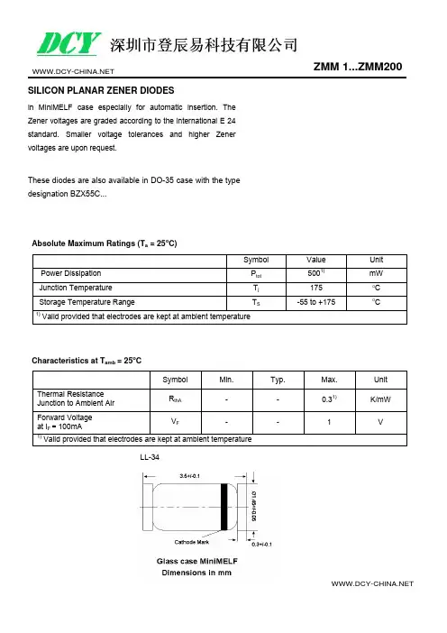
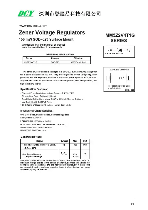
Zener Voltage Regulators150mW SOD–523Surface MountWe declare that the material of product compliance with RoHS requirements.ORDERING INFORMATIONDevice Package Shipping MM5ZXXXT1GSOD-5233000/Tape&ReelThis series of Zener diodes is packaged in a SOD–523surface mount package that has a power dissipation of 100mW.They are designed to provide voltage regulation protection and are especially attractive in situations where space is at a premium.They are well suited for applications such as cellular phones,hand held portables,and high density PC boards.Specification Features:•Standard Zener Breakdown Voltage Range –2.4V to 75V •Steady State Power Rating of 200mW•Small Body Outline Dimensions:0.047"x 0.032"(1.20mm x 0.80mm)•Low Body Height:0.028"(0.7mm)•ESD Rating of Class 3(>16kV)per Human Body ModelMechanical Characteristics:CASE:Void-free,transfer-molded,thermosetting plastic Epoxy Meets UL 94V-0LEAD FINISH:100%Matte Sn (Tin)QUALIFIED MAX REFLOW TEMPERATURE:260°C Device Meets MSL 1Requirements MOUNTING POSITION:AnyMAXIMUM RATINGSRatingSymbol Max Unit Total Device Dissipation FR−5Board,P D150mW@T A =25︒C Junction and Storage T J,Tstg−65to ︒CTemperature Range+150Maximum ratings are those values beyond which devicedamage can occur.Maximum ratings applied to the device are individual stress limit values (not normal operating conditions)and are not valid simultaneously.If these limits are exceeded,device functional operation is not implied,damage may occur and reliability may be affected.MM5Z2V4T1G SERIES12CATHODE ANODEMARKING DIAGRAMxx dxx=Specific Device Code d =Date CodeSOD–523MM5Z2V4T1G SERIES ELECTRICAL CHARACTERISTICS I(T A=25︒C unless otherwise noted,I FV F=0.9V Max.@I F=10mA for all types)Symbol ParameterVZ Reverse Zener Voltage@I ZT IZT Reverse Current VZVRVZ ZT Maximum Zener Impedance@I I R VFZT IZTIZK Reverse CurrentZZK Maximum Zener Impedance@I ZKIR Reverse Leakage Current@V RV R Reverse VoltageI F Forward Current Zener Voltage Regulator V F Forward Voltage@I FQV Z Maximum Temperature Coefficient of V ZC Max.Capacitance@V R=0and f=1MHz100(%)80DISS IP ATI ON 60 40POWER20255075100125150TEMPERATURE(︒C)Figure1.Steady State Power Derating MM5Z2V4T1G SERIESELECTRICAL CHARACTERISTICS (T A =25︒C unless otherwise noted,V F =0.9V Max.@I F =10mA for all types)Zener Voltage (Note 1)Zener Impedance Leakage CurrentQ V Z C ZZT(mV/k)@V =0V(Volts)@I@I ZT Z@II @VRZZKR@IZTf =1MHzDevice ZTZKRDevice Marking Min Nom Max mA W W mA m A Volts Min Max pF MM5Z2V4T1G 00 2.2 2.4 2.651001000 1.050 1.0−3.50450MM5Z2V7T1G 01 2.5 2.7 2.951001000 1.020 1.0−3.50450MM5Z3V0T1G 02 2.8 3.0 3.251001000 1.010 1.0−3.50450MM5Z3V3T1G 05 3.1 3.3 3.55951000 1.05 1.0−3.50450MM5Z3V6T1G 06 3.4 3.6 3.85901000 1.05 1.0−3.50450MM5Z3V9T1G 07 3.7 3.9 4.15901000 1.03 1.0−3.5−2.5450MM5Z4V3T1G 08 4.0 4.3 4.65901000 1.03 1.0−3.50450MM5Z4V7T1G 09 4.4 4.7 5.0580800 1.03 2.0−3.50.2260MM5Z5V1T1G 0A 4.8 5.1 5.4560500 1.02 2.0−2.7 1.2225MM5Z5V6T1G 0C 5.2 5.6 6.0540400 1.01 2.0−2.0 2.5200MM5Z6V2T1G 0E 5.8 6.2 6.6510100 1.03 4.00.4 3.7185MM5Z6V8T1G 0F 6.4 6.87.2515160 1.02 4.0 1.2 4.5155MM5Z7V5T1G 0G 7.07.57.9515160 1.01 5.0 2.5 5.3140MM5Z8V2T1G 0H 7.78.28.7515160 1.00.7 5.0 3.2 6.2135MM5Z9V1T1G 0K 8.59.19.6515160 1.00.27.0 3.87.0130MM5Z10VT1G 0L 9.41010.6520160 1.00.18.0 4.58.0130MM5Z11VT1G 0M 10.41111.6520160 1.00.18.0 5.49.0130MM5Z12VT1G 0N 11.41212.752580 1.00.18.0 6.010130MM5Z13VT1G 0P 12.413.2514.153080 1.00.18.07.011120MM5Z15VT1G 0T 14.31515.8530200 1.00.0510.59.213110MM5Z16VT1G 0U 15.316.217.1240200 1.00.0511.210.414105MM5Z18VT1G 0W 16.81819.1245225 1.00.0512.612.416100MM5Z20VT1G 0Z 18.82021.2255225 1.00.0514.014.41885MM5Z22VT1G 1020.82223.3255250 1.00.0515.416.42085MM5Z24VT1G 1122.824.225.6270120 1.00.0516.818.42280MM5Z27VT1G 1225.12728.9280300 1.00.0518.921.425.370MM5Z30VT1G 14283032280300 1.00.0521.024.429.470MM5Z33VT1G 18313335280300 1.00.0523.227.433.470MM5Z36VT1G 19343638290500 1.00.0525.230.437.470MM5Z39VT1G 203739412130500 1.00.0527.333.441.245MM5Z43VT1G 214043461150500 1.00.0530.137.646.640MM5Z47VT1G 1A 4447501170500 1.00.0532.942.051.840MM5Z51VT1G 1C 4851541180500 1.00.0535.746.657.240MM5Z56VT1G 1D 5256601200500 1.00.0539.252.263.840MM5Z62VT1G 1E 5862661215500 1.00.0543.458.871.635MM5Z68VT1G 1F 6468721240500 1.00.0547.665.679.835MM5Z75VT1G1G70757912555001.00.0552.573.488.6351.Zener voltage is measured with a pulse test current I Z at an ambient temperature of 25︒C.MM5Z2V4T1G SERIESSC-79/SOD-523DIMENSIONS (mm are the original dimensions)UNIT A b p c D E H E V m m0.70.350.2 1.30.9 1.70.150.50.250.11.10.71.5Note1.The marking bar indicates the cathode.OUTLINE REFERENCES EUROPEAN ISSUE DATEVERSION IECJEDECEIAJ PROJECTIONSOD523SC-7998-11-25。
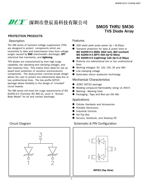
SM05 THRU SM36PROTECTION PRODUCTS TVS Diode ArrayDescriptionFeaturesCircuit Diagram Schematic & PIN ConfigurationThe SM series of transient voltage suppressors (TVS)are designed to protect components which areconnected to data and transmission lines from voltage surges caused by ESD (electrostatic discharge), EFT (electrical fast transients), and lightning .TVS diodes are characterized by their high surge capability, low operating and clamping voltages, and fast response time. This makes them ideal for use as board level protection of sensitive semiconductorcomponents. The dual-junction common-anode design allows the user to protect one bidirectional data line or two unidirectional lines. The low profile SOT23package allows flexibility in the design of crowded circuit boards.The SM series will meet the surge requirements of IEC 61000-4-2 (Formerly IEC 801-2), Level 4, Human Body Model for air and contact discharge.ApplicationsMechanical Characteristicsu Cellular Handsets and Accessories u Portable Electronics u Industrial Controls u Set-Top BoxuServers, Notebook, and Desktop PCu 300 watts peak pulse power (tp = 8/20µs)u Transient protection for data & power lines toIEC 61000-4-2 (ESD) 15kV (air), 8kV (contact)IEC 61000-4-4 (EFT) 40A (tp=5/50ns)IEC 61000-4-5 (Lightning) 12A (tp=1.2/50µs)u Protects one bidirectional line or two unidirectional linesu Working Voltages: 5V, 12V, 15V, 24 and 36V u Low clamping voltageu Solid-state silicon avalanche technologyu JEDEC SOT23 packageu Molding compound flammability rating: UL 94V-0u Marking : Marking Codeu Packaging : Tape and Reel per EIA 481Absolute Maximum RatingElectrical Characteristics50M S re t e m a r a P l o b m y S sn o i t i d n o C mu m i n i M la c i p y T mu m i x a M s t i n U e g a t l o V f f O -d n a t S e s r e v e R V M W R 5V e g a t l o V n w o d k a e r B e s r e v e R V R B I t A m 1=6V t n e r r u C e g a k a e L e s r e v e R I R V M W R C °52=T ,V 5=02A µeg a t l o V g n i p m a l C V C I P P ,A 1=s µ02/8=p t 8.9V t n e r r u C e s l u P k a e P m u m i x a M I p p s µ02/8=p t 71A e c n a t i c a p a C n o i t c n u J C j 2o t 1n i P V R z H M 1=f ,V 0=053F p ec n a t i c a p a C n o i t c n u J C jd n a 3o t 1n i P 3o t 2n i P V R zH M 1=f ,V 0=004Fp gn i t a R l o b m y S e u l a V s t i n U )s µ02/8=p t (r e w o P e s l u P k a e P P k p 003s t t a W t n e i b m A o t n o i t c n u J ,e c n a t s i s e R l a m r e h T q A J 655W /C °e r u t a r e p m e T g n i r e d l o S d a e L T L ).c e s 01(062C °e r u t a r e p m e T g n i t a r e p O T J 521+o t 55-C °er u t a r e p m e T e g a r o t S T GT S 051+o t 55-C°21M S re t e m a r a P l o b m y S sn o i t i d n o C mu m i n i M la c i p y T mu m i x a M s t i n U e g a t l o V f f O -d n a t S e s r e v e R V M W R 21V e g a t l o V n w o d k a e r B e s r e v e R V R B I t A m 1=3.31V t n e r r u C e g a k a e L e s r e v e R I R V M W R C°52=T ,V 21=1A µeg a t l o V g n i p m a l C V C I P P ,A 1=s µ02/8=p t 91V t n e r r u C e s l u P k a e P m u m i x a M I p p s µ02/8=p t 21A e c n a t i c a p a C n o i t c n u J C j 2o t 1n i P V R z H M 1=f ,V 0=021F p ec n a t i c a p a C n o i t c n u J C jd n a 3o t 1n i P 3o t 2n i P V R zH M 1=f ,V 0=051FpElectrical Characteristics (Continued)51M S re t e m a r a P l o b m y S s n o i t i d n o C m u m i n i M l a c i p y T mu m i x a M s t i n U e g a t l o V f f O -d n a t S e s r e v e R V M W R 51V e g a t l o V n w o d k a e r B e s r e v e R V R B I t A m 1=7.61Vt n e r r u C e g a k a e L e s r e v e R I R V M W R C °52=T ,V 51=1A µeg a t l o V g n i p m a l C V C I P P sµ02/8=p t ,A 1=42V t n e r r u C e s l u P k a e P m u m i x a M I p p s µ02/8=p t 01A e c n a t i c a p a C n o i t c n u J C j 2o t 1n i P V R z H M 1=f ,V 0=57F p e c n a t i c a p a C n o i t c n u J C j3o t 2d n a 3o t 1n i P V R zH M 1=f ,V 0=001Fp 42M S re t e m a r a P l o b m y S sn o i t i d n o C mu m i n i M l a c i p y T mu m i x a M s t i n U e g a t l o V f f O -d n a t S e s r e v e R V M W R 42V e g a t l o V n w o d k a e r B e s r e v e R V R B I t A m 1=7.62Vt n e r r u C e g a k a e L e s r e v e R I R V M W R C °52=T ,V 42=1A µeg a t l o V g n i p m a l C V C I P P sµ02/8=p t ,A 1=34V t n e r r u C e s l u P k a e P m u m i x a M I p p s µ02/8=p t 5A e c n a t i c a p a C n o i t c n u J C j 2o t 1n i P V R z H M 1=f ,V 0=05F p ec n a t i c a p a C n o i t c n u J C j3o t 2d n a 3o t 1n i P V R zH M 1=f ,V 0=06Fp 63M S re t e m a r a P l o b m y S s n o i t i d n o C m u m i n i M l a c i p y T mu m i x a M s t i n U e g a t l o V f f O -d n a t S e s r e v e R V M W R 63V e g a t l o V n w o d k a e r B e s r e v e R V R B I t A m 1=04Vt n e r r u C e g a k a e L e s r e v e R I R V M W R C °52=T ,V 63=1A µeg a t l o V g n i p m a l C V C I P P sµ02/8=p t ,A 1=06V t n e r r u C e s l u P k a e P m u m i x a M I p p s µ02/8=p t 4A e c n a t i c a p a C n o i t c n u J C j 2o t 1n i P V R z H M 1=f ,V 0=04F p ec n a t i c a p a C n o i t c n u J C j3o t 2d n a 3o t 1n i P V R zH M 1=f ,V 0=54FpTypical CharacteristicsNon-Repetitive Peak Pulse Power vs. Pulse Time1020304050607080901001100255075100125150Ambient Temperature - T A (oC)% o f R a t e d P o w e r o r I P PPower Derating CurvePulse Waveform0102030405060708090100110051015202530Time (µs)P e r c e n t o f I P Ple v e L t s r i F k a e P t n e r r u C )A (k a e P t n e r r u C s n 03t a )A (k a e P t n e r r u C s n 06t a )A (t s eT eg a t l o V tc a t n o C ()e g r a h c s i D )V k (ts e T e g a t l o V r i A ()e g r a h c s i D )V k (15.74822251844435.2221668436188510.010.11100.11101001000Pulse Duration - tp (µs)P e a k P u l s e P o w e r - P P P (k W )IEC 61000-4-2 Discharge ParametersESD Pulse Waveform (Per IEC 61000-4-2)Applications InformationDevice Schematic & Pin Configuration Device Connection OptionsThe SM series is designed to protect one bidirectionalor two unidirectional data or I/O lines operating at 5 to36 volts. Connection options are as follows:l Bidirectional: Pin 1 is connected to the data lineand pin 2 is connected to ground (Since the deviceis symmetrical, these connections may be re-versed). For best results, the ground connectionshould be made directly to a ground plane on theboard. The path length should be kept as short aspossible to minimize parasitic inductance. Pin 3 isnot connected.l Unidirectional: Data lines are connected to pin 1 and pin 2. Pin 3 is connected to ground. For best results, this pin should be connected directly to aground plane on the board. The path length should be kept as short as possible to minimize parasiticinductance.Circuit Board Layout Recommendations for Suppres-sion of ESD.Good circuit board layout is critical for the suppression of fast rise-time transients such as ESD. The following guidelines are recommended (Refer to application note SI99-01 for more detailed information):l Place the TVS near the input terminals or connec-tors to restrict transient coupling.l Minimize the path length between the TVS and the protected line.l Minimize all conductive loops including power and ground loops.l The ESD transient return path to ground should be kept as short as possible.l Never run critical signals near board edges.l Use ground planes whenever possible.RS-232 Transceiver ProtectionExampleOutline Drawing - SOT23Ordering Informationr e b m u N t r a P g n i k r o W e g a t l o V le e R r e p y t Q e z i S l e e R C T .50M S V 5000,3h c n I 7G T .50M S V 5000,01h c n I 31C T .21M S V 21000,3h c n I 7G T .21M S V 21000,01h c n I 31C T .51M S V 51000,3h c n I 7G T .51M S V 51000,01h c n I 31C T .42M S V 42000,3h c n I 7G T .42M S V 42000,01h c n I 31CT .63M S V63000,3hc n I 7Marking Codesre b m u N t r a P g n i k r a M e d o C 50M S 50M 21M S 21M 51M S 51M 42M S 42M 63M S 63M。
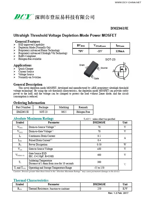
DMZ0615EUltrahigh Threshold Voltage Depletion-Mode Power MOSFETGeneral FeaturesESD improved CapabilityDepletion Mode (Normally On)Proprietary Advanced Planar TechnologyProprietary Advanced Ultrahigh Vth Technology RoHS CompliantHalogen-free availableApplicationsQuick Charger Current Source Voltage SourceNormally-on SwitchesGeneral DescriptionThis novel depletion mode MOSFET, developed and manufactured by ARK proprietary ultrahigh threshold voltage technology. By using the sub threshold characteristics, the depletion mode MOSFET can provide stably power to the load, and the voltage can be clamped to protect the load without Zener diode, and the circuit consumption is reduced.DrainGateSourceSOT-23NOTE:[1] T J=+25℃to +150℃[2] Repetitive rating, pulse width limited by maximum junction temperature.[3] Pulse width≤380µs; duty cycle≤2%.Rev. 1.2 Feb. 2017Rev. 1.2 Feb. 2017Depletion mode MOSFET has the function of providing power for IC in circuit, as shown in Figure 3.Figure 3The parameters of the depletion mode MOSFET and the resistance (R L) of the IC are jointly determined the voltage(V out) and current(I D) supplied to the IC.I D = I DSS(1+I D R L/V GS(OFF))2V out = -V GS = I D R LFigure 4By this way, the depletion mode MOSFET operate in sub-threshold region, the gate voltage(V GS) is always at or below threshold voltage(V GS(OFF)), even when the input voltage(V in) is increased or the peak voltage occurs also so. Therefore, in addition to provide power for IC, the device can clamp voltage, the IC is protected. The V out and V in have the following formula:If V in <∣V GS(OFF)∣, then V out ≈V inIf V in ≥∣V GS(OFF)∣, then V out ≤V GS(OFF)The Ultrahigh Threshold Voltage Depletion-Mode Power MOSFET--DMZ0615E, was developed by ARK Microelectronics using proprietary technology. The threshold voltage of DMZ0615E exceeds -16V, can provide sufficient voltage for IC.Rev. 1.2 Feb. 2017In the QC2.0/3.0 and Type-C charger circuits, using the depletion mode MOSFET can make the PWM IC power supply circuit more simplified, as shown below:In Figure 5, the transistor Q3 is used to provide power, and the zener diode ZD is used to clamp voltage, the power supply circuit of IC is composed of several components.PWM ICFigure 5In figure 6, providing power and clamp voltage use only one device-DMZ0615E, the circuit is simplified.PWM ICFigure 6Rev. 1.2 Feb. 2017Rev. 1.2 Feb. 2017。
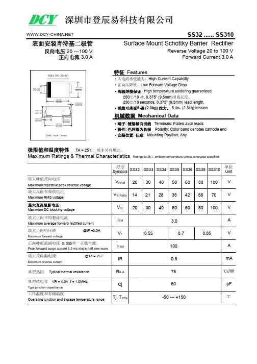
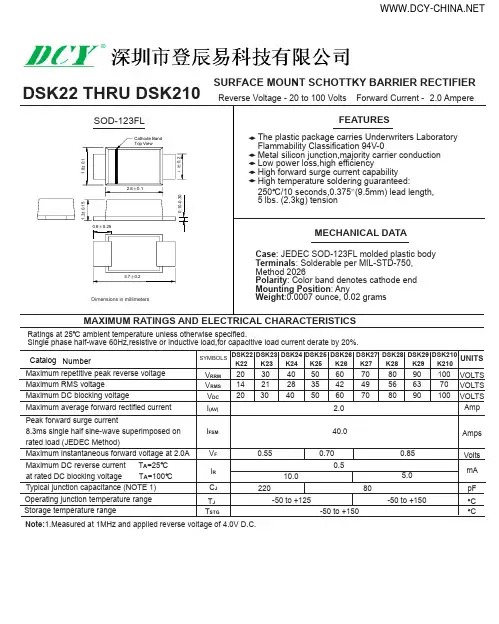
SS32 ...... SS310表面安装肖特基二极管反向电压 20 ---100 V正向电流 3.0 A极限值和温度特性 TA = 25℃ 除非另有规定。
Maximum Ratings & Thermal CharacteristicsRatings at 25℃ ambient temperature unless otherwise specified.Surface Mount Schottky Barrier RectifierReverse Voltage 20 to 100 VForward Current 3.0 A·正向压降低。
Low Forward Voltage Drop·大电流承受能力。
High Current Capability ·高温焊接保证 High temperature soldering guaranteed:250℃/10 秒, 0.375" (9.5mm)引线长度。
250℃/10 seconds, 0.375" (9.5mm) lead length,·引线可承受5 磅 (2.3kg) 拉力。
5 lbs. (2.3kg) tension机械数据 Mechanical Data·端子: 镀锡轴向引线 Terminals: Plated axial leads·极性: 色环端为负极 Polarity: Color band denotes cathode end ·安装位置: 任意 Mounting Position: Any特征 FeaturesSS32 3.01000.57520140.550.8560V V ℃AV A mA ℃//W pF 单位UnitV V R(RMS)最大正向平均整流电流最大峰值反向电压最大反向有效值电压-50 --- +150V RRM I FM 最大正向电压降 @IF =3.0AV F 正向峰值浪涌电流 8.3mS单一正弦半波I FSM 最大反向漏电流IR 典型热阻工作温度和存储温度R θJA Tj, T STG典型结电容 VR = 4.0V f = 1.0MHzCj @TA = 25℃Maximum repetitive peak reverse voltageMaximum RMS voltage最大直流阻断电压Maximum DC blocking voltageMaximum average forward rectified currentMaximum forward voltagePeak forward surge current 8.3 ms single half sine-waveMaximum reverse currentTypical thermal resistanceOperating junction and storage temperature rangeType junction capacitance符号SymbolsV DC 20SS33SS34SS35SS36SS38SS310302130402840503550604260805680100701000.7正向电流 I F (A )正向特性曲线(典型值)正向电压 V F (V)环境温度 Ta(°C )通过电流的周期峰值正向浪涌电流 I F S M (A )平均正向电流 I F (A V ) (A )浪涌特性曲线(最大值)TYPICAL FORWARD CHARACTERISTICFORWARD CURRENT DERATING CURVEI F I n s t a n t a n e o u s F o r w a r d C u r r e n t (A )V F Instantaneous Forward Voltage (V)Tamb, ambient temperature (°C)I F (A ) A v e r a g e F o r w a r d R e c t i f i e d C u r r e n t (A )MAXIMUM NON REPETITIVE PEAK FORWARD SURGE CURRENTNumber of Cycles at 60 Hz.I F S M P e a k F o r w a r d S u r g e C u r r e n t (A )正向电流降额曲线0.010.1110500.6 1.2 1.602550751001251501753.02.52.01.51.00.501246102040100806040200100峰值反向电压百分比(%)TYPICAL REVERSE CHARACTERISTICSPercent Of Peak Reverse Voltage,%I R I n s t a n t a n e o u s R e v e r s e C u r r e n t (µA )反向特性曲线(典型值)反向电流 I R (μA )0.0010.010.11080140T J =125°CT J =25°C2040601001201.00.20.8 1.40.4SS32 ...... SS310特性曲线 Characteristic CurvesT J =75°C120SS32-SS34SS35-SS36SS38-SS310。
Zener Voltage Regulators150mW SOD–523Surface MountWe declare that the material of product compliance with RoHS requirements.ORDERING INFORMATIONDevice Package Shipping MM5ZXXXT1GSOD-5233000/Tape&ReelThis series of Zener diodes is packaged in a SOD–523surface mount package that has a power dissipation of 100mW.They are designed to provide voltage regulation protection and are especially attractive in situations where space is at a premium.They are well suited for applications such as cellular phones,hand held portables,and high density PC boards.Specification Features:•Standard Zener Breakdown Voltage Range –2.4V to 75V •Steady State Power Rating of 200mW•Small Body Outline Dimensions:0.047"x 0.032"(1.20mm x 0.80mm)•Low Body Height:0.028"(0.7mm)•ESD Rating of Class 3(>16kV)per Human Body ModelMechanical Characteristics:CASE:Void-free,transfer-molded,thermosetting plastic Epoxy Meets UL 94V-0LEAD FINISH:100%Matte Sn (Tin)QUALIFIED MAX REFLOW TEMPERATURE:260°C Device Meets MSL 1Requirements MOUNTING POSITION:AnyMAXIMUM RATINGSRatingSymbol Max Unit Total Device Dissipation FR−5Board,P D150mW@T A =25︒C Junction and Storage T J,Tstg−65to ︒CTemperature Range+150Maximum ratings are those values beyond which devicedamage can occur.Maximum ratings applied to the device are individual stress limit values (not normal operating conditions)and are not valid simultaneously.If these limits are exceeded,device functional operation is not implied,damage may occur and reliability may be affected.MM5Z2V4T1G SERIES12CATHODE ANODEMARKING DIAGRAMxx dxx=Specific Device Code d =Date CodeSOD–523MM5Z2V4T1G SERIES ELECTRICAL CHARACTERISTICS I(T A=25︒C unless otherwise noted,I FV F=0.9V Max.@I F=10mA for all types)Symbol ParameterVZ Reverse Zener Voltage@I ZT IZT Reverse Current VZVRVZ ZT Maximum Zener Impedance@I I R VFZT IZTIZK Reverse CurrentZZK Maximum Zener Impedance@I ZKIR Reverse Leakage Current@V RV R Reverse VoltageI F Forward Current Zener Voltage Regulator V F Forward Voltage@I FQV Z Maximum Temperature Coefficient of V ZC Max.Capacitance@V R=0and f=1MHz100(%)80DISS IP ATI ON 60 40POWER20255075100125150TEMPERATURE(︒C)Figure1.Steady State Power Derating MM5Z2V4T1G SERIESELECTRICAL CHARACTERISTICS (T A =25︒C unless otherwise noted,V F =0.9V Max.@I F =10mA for all types)Zener Voltage (Note 1)Zener Impedance Leakage CurrentQ V Z C ZZT(mV/k)@V =0V(Volts)@I@I ZT Z@II @VRZZKR@IZTf =1MHzDevice ZTZKRDevice Marking Min Nom Max mA W W mA m A Volts Min Max pF MM5Z2V4T1G 00 2.2 2.4 2.651001000 1.050 1.0−3.50450MM5Z2V7T1G 01 2.5 2.7 2.951001000 1.020 1.0−3.50450MM5Z3V0T1G 02 2.8 3.0 3.251001000 1.010 1.0−3.50450MM5Z3V3T1G 05 3.1 3.3 3.55951000 1.05 1.0−3.50450MM5Z3V6T1G 06 3.4 3.6 3.85901000 1.05 1.0−3.50450MM5Z3V9T1G 07 3.7 3.9 4.15901000 1.03 1.0−3.5−2.5450MM5Z4V3T1G 08 4.0 4.3 4.65901000 1.03 1.0−3.50450MM5Z4V7T1G 09 4.4 4.7 5.0580800 1.03 2.0−3.50.2260MM5Z5V1T1G 0A 4.8 5.1 5.4560500 1.02 2.0−2.7 1.2225MM5Z5V6T1G 0C 5.2 5.6 6.0540400 1.01 2.0−2.0 2.5200MM5Z6V2T1G 0E 5.8 6.2 6.6510100 1.03 4.00.4 3.7185MM5Z6V8T1G 0F 6.4 6.87.2515160 1.02 4.0 1.2 4.5155MM5Z7V5T1G 0G 7.07.57.9515160 1.01 5.0 2.5 5.3140MM5Z8V2T1G 0H 7.78.28.7515160 1.00.7 5.0 3.2 6.2135MM5Z9V1T1G 0K 8.59.19.6515160 1.00.27.0 3.87.0130MM5Z10VT1G 0L 9.41010.6520160 1.00.18.0 4.58.0130MM5Z11VT1G 0M 10.41111.6520160 1.00.18.0 5.49.0130MM5Z12VT1G 0N 11.41212.752580 1.00.18.0 6.010130MM5Z13VT1G 0P 12.413.2514.153080 1.00.18.07.011120MM5Z15VT1G 0T 14.31515.8530200 1.00.0510.59.213110MM5Z16VT1G 0U 15.316.217.1240200 1.00.0511.210.414105MM5Z18VT1G 0W 16.81819.1245225 1.00.0512.612.416100MM5Z20VT1G 0Z 18.82021.2255225 1.00.0514.014.41885MM5Z22VT1G 1020.82223.3255250 1.00.0515.416.42085MM5Z24VT1G 1122.824.225.6270120 1.00.0516.818.42280MM5Z27VT1G 1225.12728.9280300 1.00.0518.921.425.370MM5Z30VT1G 14283032280300 1.00.0521.024.429.470MM5Z33VT1G 18313335280300 1.00.0523.227.433.470MM5Z36VT1G 19343638290500 1.00.0525.230.437.470MM5Z39VT1G 203739412130500 1.00.0527.333.441.245MM5Z43VT1G 214043461150500 1.00.0530.137.646.640MM5Z47VT1G 1A 4447501170500 1.00.0532.942.051.840MM5Z51VT1G 1C 4851541180500 1.00.0535.746.657.240MM5Z56VT1G 1D 5256601200500 1.00.0539.252.263.840MM5Z62VT1G 1E 5862661215500 1.00.0543.458.871.635MM5Z68VT1G 1F 6468721240500 1.00.0547.665.679.835MM5Z75VT1G1G70757912555001.00.0552.573.488.6351.Zener voltage is measured with a pulse test current I Z at an ambient temperature of 25︒C.MM5Z2V4T1G SERIESSC-79/SOD-523DIMENSIONS (mm are the original dimensions)UNIT A b p c D E H E V m m0.70.350.2 1.30.9 1.70.150.50.250.11.10.71.5Note1.The marking bar indicates the cathode.OUTLINE REFERENCES EUROPEAN ISSUE DATEVERSION IECJEDECEIAJ PROJECTIONSOD523SC-7998-11-25。