CD4508BM96,CD4508BM96,CD4508BE,CD4508BNSR,CD4508BNSR,CD4508BNSR,CD4508BM96E4, 规格书,Datasheet 资料
- 格式:pdf
- 大小:902.23 KB
- 文档页数:18

电路原理和原理图:调频收音机具有灵敏度高、选择性好、通频带宽、音质好等特点。
采用CD9088调频专用集成电路来制作电调谐调频收音机,具有电路简单、制作容易、调试方便、性能价格比高、音质好、成本低、体积小等特点。
CD9088采用16脚双列扁平封装,可直接焊接在印刷电路板上,其工作电压范围为 1.8〜5V,典型值为3V。
该电路内含调频收音机从天线接收到鉴频级输岀音频信号的全部功能,并设有搜索调谐电路,信号检测电路,静噪电路,以及频率锁定环(FLL)电路等。
其特点是采用70KHZ中频频率,不设置外围中频变压器,中频选择性由RC中频滤波器来完成,简化了电路、省去了中频频率调试的麻烦,又提高了中频频率特性,并减少了电路体积。
用CD9088可组成各种调频收音机电路,除可采用电调谐方式来搜索电台外,也可采用传统的可变电容器调谐搜索电台。
CD9088集成电路各引脚的功能如下表:有关收音机原理还可以参考以下资料:FM 信号由天线引进后从CD9088集成块11脚进入混频电路,电感L1、电阻 R1、电容C1、C2、C3构成输入回路,本振电路的本振频率由 L2、C4及变容二极 管D1决定。
C7为音频静噪电容,C8为中频反馈电容,C9为低通滤波器电容, C10为中频级耦合电容,15脚为搜索调谐端,16脚为电调谐AFC 电压输出端, SB1为复位按钮,SB2为调谐按钮。
按一下SB2按钮收音机就会自动从频率低端 向频率高端选台,当收到一个电台时,便自动锁定电台停止搜索,如要收听下一 个电台节目,可再按一下SB2按钮顺序搜索电台。
当搜索到频率最高端时,按一 下SB1按钮即可回到频率最低端,然再重新选台。
天线输入回路收到的电台信号与本振频率混频后产生70kHz 中频信号。
经RC 中频滤波器完成滤波和放大后送鉴频级处理,然输出音频复合信号,通过静 噪电路后,从CD9088的2脚输出音频复合信号,经 R3 C15去加重电路后,由 C16耦合到由VT1、VT2组成的低频放大电路放大,推动耳机放音。
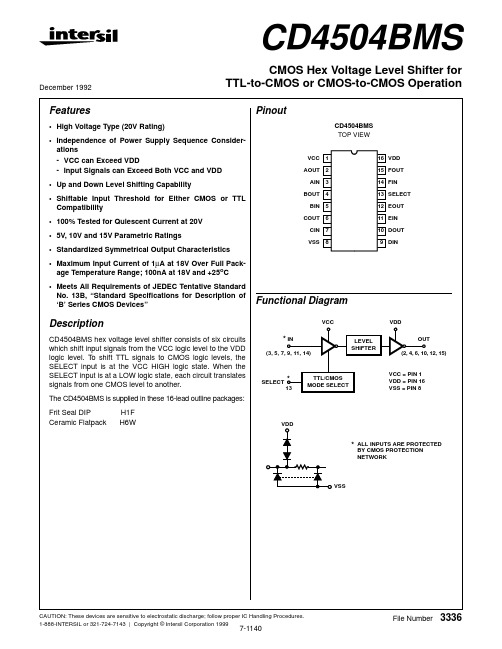
CAUTION: These devices are sensitive to electrostatic discharge; follow proper IC Handling Procedures.CD4504BMSCMOS Hex Voltage Level Shifter forTTL-to-CMOS or CMOS-to-CMOS OperationFeatures•High Voltage Type (20V Rating)•Independence of Power Supply Sequence Consider-ations-VCC can Exceed VDD-Input Signals can Exceed Both VCC and VDD •Up and Down Level Shifting Capability•Shiftable Input Threshold for Either CMOS or TTL Compatibility •100% Tested for Quiescent Current at 20V •5V, 10V and 15V Parametric Ratings•Standardized Symmetrical Output Characteristics •Maximum Input Current of 1µA at 18V Over Full Pack-age Temperature Range; 100nA at 18V and +25o C •Meets All Requirements of JEDEC Tentative Standard No. 13B, “Standard Specifications for Description of ‘B’ Series CMOS Devices”DescriptionCD4504BMS hex voltage level shifter consists of six circuits which shift input signals from the VCC logic level to the VDD logic level. To shift TTL signals to CMOS logic levels, the SELECT input is at the VCC HIGH logic state. When the SELECT input is at a LOW logic state, each circuit translates signals from one CMOS level to another.The CD4504BMS is supplied in these 16-lead outline packages:Frit Seal DIPH1F Ceramic FlatpackH6WDecember 1992File Number3336PinoutCD4504BMS TOP VIEWFunctional Diagram14151691312111012345768VCC AOUT AIN BOUT BIN COUT VSSCIN VDD FIN SELECT EOUT EIN DOUT DINFOUT TTL/CMOS MODE SELECTLEVEL SHIFTEROUT (2, 4, 6, 10, 12, 15)(3, 5, 7, 9, 11, 14)* IN*13SELECTVCC = PIN 1VDD = PIN 16VSS = PIN 8VDDVSS*ALL INPUTS ARE PROTECTED BY CMOS PROTECTION NETWORKVCCVDDAbsolute Maximum Ratings Reliability InformationDC Supply Voltage Range, (VDD) . . . . . . . . . . . . . . .-0.5V to +20V (Voltage Referenced to VSS Terminals)Input Voltage Range, All Inputs . . . . . . . . . . . . .-0.5V to VDD +0.5V DC Input Current, Any One Input . . . . . . . . . . . . . . . . . . . . . . . .±10mA Operating Temperature Range. . . . . . . . . . . . . . . .-55o C to +125o C Package Types D, F, K, HStorage Temperature Range (TSTG). . . . . . . . . . .-65o C to +150o C Lead Temperature (During Soldering) . . . . . . . . . . . . . . . . .+265o C At Distance 1/16 ± 1/32 Inch (1.59mm± 0.79mm) from case for 10s Maximum Thermal Resistance . . . . . . . . . . . . . . . .θjaθjc Ceramic DIP and FRIT Package. . . . .80o C/W20o C/W Flatpack Package . . . . . . . . . . . . . . . .70o C/W20o C/W Maximum Package Power Dissipation (PD) at +125o CFor TA = -55o C to +100o C (Package Type D, F, K). . . . . .500mW For TA = +100o C to +125o C (Package Type D, F, K) . . . . .DerateLinearity at 12mW/o C to 200mW Device Dissipation per Output Transistor . . . . . . . . . . . . . . .100mW For TA = Full Package Temperature Range (All Package Types) Junction Temperature . . . . . . . . . . . . . . . . . . . . . . . . . . . . . .+175o CTABLE1.DC ELECTRICAL PERFORMANCE CHARACTERISTICSPARAMETER SYMBOL CONDITIONS(NOTE 1)GROUP ASUBGROUPS TEMPERATURELIMITSUNITSMIN MAXSupply Current IDD VDD = 20V, VIN = VDD or GND1+25o C-2µA2+125o C-200µAVDD = 18V, VIN = VDD or GND3-55o C-2µA Input Leakage Current IIL VIN = VDD or GND VDD = 201+25o C-100-nA2+125o C-1000-nAVDD = 18V3-55o C-100-nA Input Leakage Current IIH VIN = VDD or GND VDD = 201+25o C-100nA2+125o C-1000nAVDD = 18V3-55o C-100nA Output Voltage VOL15VDD = 15V, No Load1, 2, 3+25o C, +125o C, -55o C-50mV Output Voltage VOH15VDD = 15V, No Load (Note 3)1, 2, 3+25o C, +125o C, -55o C14.95-V Output Current (Sink)IOL5VDD = 5V, VOUT = 0.4V1+25o C0.53-mA Output Current (Sink)IOL10VDD = 10V, VOUT = 0.5V1+25o C 1.4-mA Output Current (Sink)IOL15VDD = 15V, VOUT = 1.5V1+25o C 3.5-mA Output Current (Source)IOH5A VDD = 5V, VOUT = 4.6V1+25o C--0.53mA Output Current (Source)IOH5B VDD = 5V, VOUT = 2.5V1+25o C--1.8mA Output Current (Source)IOH10VDD = 10V, VOUT = 9.5V1+25o C--1.4mA Output Current (Source)IOH15VDD = 15V, VOUT = 13.5V1+25o C--3.5mA N Threshold Voltage VNTH VDD = 10V, ISS = -10µA1+25o C-2.8-0.7V P Threshold Voltage VPTH VSS = 0V, IDD = 10µA1+25o C0.7 2.8VFunctional F VDD = 4.5V, VCC = 2.8,VIN = VDD or GND 7+25o C VOH >VDD/2VOL <VDD/2VVDD = 4.5V, VCC = 3.0,VIN = VDD or GND8B-55o CVDD = 18V, VCC = 18V,VIN = GND or VCC8A+125o CVDD = 18V, VCC = 4.5V,VIN = VCC or GND8A+125o CVDD = 4.5V, VCC = 18V,VIN = VCC or GND8A+125o CVDD = 20V, VCC = 20V,VIN = GND or VCC7+25o CVDD = 20V, VCC = 4.5V,VIN = VCC or GND7+25o CVDD = 4.5V, VCC = 20V,VIN = VCC or GND7+25o CInput Voltage Low (Note 2) TTL-CMOS VIL VDD = 15V, VOH > 13.5V, VOL < 1V VCC = 5V1, 2, 3+25o C, +125o C, -55o C -0.8V Input Voltage High (Note 2) TTL-CMOS VIH VDD = 15V, VOH > 13.5V, VOL < 1V VCC = 5V1, 2, 3+25o C, +125o C, -55o C 2-V Input Voltage Low(Note 2) CMOS-CMOS VIL VDD = 10V, VOH > 9V, VOL < 1V VCC = 5V1, 2, 3+25o C, +125o C, -55o C - 1.5V Input Voltage High (Note 2)CMOS-CMOS VIH VDD = 10V, VOH > 9V, VOL < 1V VCC = 5V1, 2, 3+25o C, +125o C, -55o C 3.5-V Input Voltage Low(Note 2) CMOS-CMOS VIL VDD = 15V, VOH > 13.5V, VOL <1.5V, VCC = 10V1, 2, 3+25o C, +125o C, -55o C -3V Input Voltage High (Note 2) CMOS-CMOSVIHVDD = 15V, VOH > 13.5V, VOL <1.5V, VCC = 10V1, 2, 3+25o C, +125o C, -55o C7-VNOTES: 1.All voltages referenced to device GND, 100% testing beingimplemented.2.Go/No Go test with limits applied to inputs.3.For accuracy, voltage is measured differentially to VDD. Limit is 0.050V max.TABLE 2.AC ELECTRICAL PERFORMANCE CHARACTERISTICSPARAMETER SYMBOL CONDITIONS (NOTE 1, 2)GROUP ASUBGROUPS TEMPERATURELIMITS UNITS MIN MAX Propagation Delay TTL to CMOS VDD > VCCTPHL1VDD = 10V, VIN = VCC or GND VCC = 5V9+25o C -280ns 10, 11+125o C, -55o C-378ns Propagation DelayCMOS to CMOS VDD >VCCTPHL2VDD = 10V, VIN = VCC or GND VCC = 5V9+25o C -240ns 10, 11+125o C, -55o C-324ns Propagation DelayCMOS to CMOS VCC >VDDTPHL3VDD = 5V, VIN = VCC or GND VCC = 10V9+25o C -550ns 10, 11+125o C, -55o C-743ns Propagation Delay TTL to CMOS VDD > VCCTPLH1VDD = 10V, VIN = VCC or GND VCC = 5V9+25o C -280ns 10, 11+125o C, -55o C-378ns Propagation DelayCMOS to CMOS VDD >VCCTPLH2VDD = 10V, VIN = VCC or GND VCC = 5V9+25o C -240ns 10, 11+125o C, -55o C-324ns Propagation DelayCMOS to CMOS VCC >VDDTPLH3VDD = 5V, VIN = VCC or GND VCC = 10V 9+25o C -400ns 10, 11+125o C, -55o C-540ns Transition TimeTTHL TTLHAll Modes9+25o C -200ns 10, 11+125o C, -55o C-270nsNOTES:1.CL = 50pF, RL = 200K, Input TR, TF < 20ns.2.-55o C and +125o C limits guaranteed, 100% testing being implemented.TABLE 1.DC ELECTRICAL PERFORMANCE CHARACTERISTICS (Continued)PARAMETER SYMBOL CONDITIONS (NOTE 1)GROUP A SUBGROUPSTEMPERATURE LIMITSUNITS MIN MAXTABLE3.ELECTRICAL PERFORMANCE CHARACTERISTICSPARAMETER SYMBOL CONDITIONS NOTES TEMPERATURELIMITSUNITS MIN MAXSupply Current IDD VDD = 5V, VIN = VDD or GND1, 2-55o C, +25o C-1µA+125o C-30µAVDD = 10V, VIN = VDD or GND1, 2-55o C, +25o C-2µA+125o C-60µAVDD = 15V, VIN = VDD or GND1, 2-55o C, +25o C-2µA+125o C-120µA Output Voltage VOL VDD = 5V, No Load1, 2+25o C, +125o C,-55o C-50mVOutput Voltage VOL VDD = 10V, No Load1, 2+25o C, +125o C,-55o C-50mVOutput Voltage VOH VDD = 5V, No Load1, 2+25o C, +125o C,-55o C4.95-VOutput Voltage VOH VDD = 10V, No Load1, 2+25o C, +125o C,-55o C9.95-V Output Current (Sink)IOL5VDD = 5V, VOUT = 0.4V1, 2+125o C0.36-mA-55o C0.64-mA Output Current (Sink)IOL10VDD = 10V, VOUT = 0.5V1, 2+125o C0.9-mA-55o C 1.6-mA Output Current (Sink)IOL15VDD = 15V, VOUT = 1.5V1, 2+125o C 2.4-mA-55o C 4.2-mA Output Current (Source)IOH5A VDD = 5V, VOUT = 4.6V1, 2+125o C--0.36mA-55o C--0.64mA Output Current (Source)IOH5B VDD = 5V, VOUT = 2.5V1, 2+125o C--1.15mA-55o C--2.0mA Output Current (Source)IOH10VDD = 10V, VOUT = 9.5V1, 2+125o C--0.9mA-55o C--1.6mA Output Current (Source)IOH15VDD =15V, VOUT = 13.5V1, 2+125o C--2.4mA-55o C--4.2mAInput Voltage Low TTL - CMOS VIL VDD = 10V, VOH > 9V,VOL < 1V, VCC = 5V1, 2+25o C, +125o C,-55o C-0.8VInput Voltage High TTL - CMOS VIH VDD = 10V, VOH > 9V,VOL < 1V, VCC = 5V1, 2+25o C, +125o C,-55o C2-VInput Voltage Low CMOS - CMOS VIL VDD = 15V, VOH > 13.5V,VOL < 1.5V, VCC = 5V1, 2+25o C, +125o C,-55o C- 1.5VInput Voltage High CMOS - CMOS VIH VDD = 15V, VOH > 13.5V,VOL < 1.5V, VCC = 5V1, 2+25o C, +125o C,-55o C3.5-VPropagation DelayTTL - CMOS, VDD > VCCTPHL1VDD = 15V, VCC = 5V1, 2, 3+25o C-280nsPropagation Delay CMOS - CMOS, VDD > VCC TPHL2VDD = 15V, VCC = 5V1, 2, 3+25o C-240ns VDD = 15V, VCC = 10V1, 2, 3+25o C-140nsPropagation Delay CMOS - CMOS, VCC > VDD TPHL3VDD = 5V, VCC = 15V1, 2, 3+25o C-550ns VDD = 10V, VCC = 15V1, 2, 3+25o C-140nsPropagation DelayTTL - CMOS, VDD > VCCTPLH1VDD = 15V, VCC = 5V1, 2, 3+25o C-280nsPropagation Delay CMOS - CMOS,VDD > VCC TPLH2VDD = 15V, VCC = 5V 1, 2, 3+25o C -240ns VDD = 15V, VCC = 10V1, 2, 3+25o C -140ns Propagation Delay CMOS - CMOS VCC > VDD TPLH3VDD = 5V, VCC = 15V 1, 2, 3+25o C -400ns VDD = 10V, VCC = 15V1, 2, 3+25o C -120ns Transition TimeTTHL TTLH VDD = 10V 1, 2, 3+25o C -100ns VDD = 15V 1, 2, 3+25o C -80ns Input Capacitance CINAny Input1, 2+25o C-7.5pFNOTES:1.All voltages referenced to device GND.2.The parameters listed on Table 3 are controlled via design or process and are not directly tested. These parameters are characterized on initial design release and upon design changes which would affect these characteristics.3.CL = 50pF, RL = 200K, Input TR, TF < 20ns.TABLE 4.POST IRRADIATION ELECTRICAL PERFORMANCE CHARACTERISTICSPARAMETER SYMBOL CONDITIONSNOTES TEMPERATURELIMITSUNITS MIN MAX Supply Current IDD VDD = 20V, VIN = VDD or GND 1, 4+25o C -7.5µA N Threshold Voltage VNTH VDD = 10V, ISS = -10µA 1, 4+25o C -2.8-0.2V N Threshold Voltage Delta∆VTN VDD = 10V, ISS = -10µA 1, 4+25o C -±1V P Threshold Voltage VTP VSS = 0V, IDD = 10µA 1, 4+25o C 0.2 2.8V P Threshold Voltage Delta ∆VTP VSS = 0V, IDD = 10µA1, 4+25o C -±1V FunctionalFVDD = 18V, VIN = VDD or GND 1+25o CVOH >VDD/2VOL <VDD/2VVDD = 3V, VIN = VDD or GNDPropagation Delay TimeTPHL TPLHVDD = 5V1, 2, 3, 4+25o C- 1.35 x +25o C LimitnsNOTES: 1.All voltages referenced to device GND.2.CL = 50pF, RL = 200K, Input TR, TF < 20ns.3.See Table 2 for +25o C limit.4.Read and RecordTABLE 5.BURN-IN AND LIFE TEST DELTA PARAMETERS +25o C PARAMETERSYMBOL DELTA LIMITSupply Current - MSI-1IDD ± 0.2µAOutput Current (Sink)IOL5± 20% x Pre-Test Reading Output Current (Source)IOH5A± 20% x Pre-Test ReadingTABLE 6.APPLICABLE SUBGROUPSCONFORMANCE GROUP MIL-STD-883METHOD GROUP A SUBGROUPSREAD AND RECORD Initial Test (Pre Burn-In)100% 50041, 7, 9IDD, IOL5, IOH5A Interim Test 1 (Post Burn-In)100% 50041, 7, 9IDD, IOL5, IOH5A Interim Test 2 (Post Burn-In)100% 50041, 7, 9IDD, IOL5, IOH5APDA (Note 1)100% 50041, 7, 9, DeltasTABLE 3.ELECTRICAL PERFORMANCE CHARACTERISTICS (Continued)PARAMETER SYMBOL CONDITIONSNOTES TEMPERATURELIMITSUNITS MIN MAXInterim Test 3 (Post Burn-In)100% 50041, 7, 9IDD, IOL5, IOH5APDA (Note 1)100% 50041, 7, 9, Deltas Final Test 100% 50042, 3, 8A, 8B, 10, 11Group A Sample 50051, 2, 3, 7, 8A, 8B, 9, 10, 11Group BSubgroup B-5Sample 50051, 2, 3, 7, 8A, 8B, 9, 10, 11, DeltasSubgroups 1, 2, 3, 9, 10, 11Subgroup B-6Sample 50051, 7, 9Group DSample 50051, 2, 3, 8A, 8B, 9Subgroups 1, 2 3NOTE:1. 5% Parameteric, 3% Functional; Cumulative for Static 1 and 2.TABLE 7.TOTAL DOSE IRRADIATIONCONFORMANCE GROUPS MIL-STD-883METHODTESTREAD AND RECORD PRE-IRRAD POST-IRRAD PRE-IRRADPOST-IRRAD Group E Subgroup 250051, 7, 9Table 41, 9Table 4TABLE 8.BURN-IN AND IRRADIATION TEST CONNECTIONSFUNCTION OPEN GROUND VDD 9V ± -0.5V OSCILLATOR50kHz25kHzStatic Burn-In 1(Note 1)2, 4, 6, 10, 12, 153, 5, 7-9, 11, 14161, 13Static Burn-In 2(Note 1)2, 4, 6, 10, 12, 158161, 3, 5, 7, 9, 11,13, 14Dynamic Burn-In (Note 1, 3)-8161, 2, 4, 6, 10, 12,153, 5, 7, 9, 11, 14Irradiation (Note 2)2, 4, 6, 10, 12, 1581, 3, 5, 7, 9, 11, 13,14, 16NOTES:1.Each pin except VCC, VDD and GND will have a series resistor of 10K ± 5%, VDD = 18V ± 0.5V2.Each pin except VCC, VDD and GND will have a series resistor of 47K ±5%; Group E, Subgroup 2, sample size is 4 dice/wafer, 0 failures,VDD = 10V ± 0.5V3.Oscillator output to be VDD/2.TABLE 6.APPLICABLE SUBGROUPS (Continued)CONFORMANCE GROUP MIL-STD-883METHOD GROUP A SUBGROUPSREAD AND RECORDTypical Performance CharacteristicsFIGURE 1.TYPICAL OUTPUT LOW (SINK) CURRENTCHARACTERISTICSFIGURE 2.MINIMUM OUTPUT LOW (SINK) CURRENTCHARACTERISTICSFIGURE 3.TYPICAL OUTPUT HIGH (SOURCE) CURRENTCHARACTERISTICSFIGURE 4.MINIMUM OUTPUT HIGH (SOURCE) CURRENTCHARACTERISTICSFIGURE 5.TYPICAL INPUT SWITCHING AS A FUNCTION OFHIGH LEVEL SUPPLY VOLTAGE (SELECT AT VCC-CMOS MODE)FIGURE 6.TYPICAL INPUT SWITCHING AS A FUNCTION OFHIGH LEVEL SUPPLY VOLTAGE (SELECT AT VSS-TTL MODE)10V5VAMBIENT TEMPERATURE (T A ) = +25o CGATE-TO-SOURCE VOLTAGE (VGS) = 15V51015151********DRAIN-TO-SOURCE VOLTAGE (VDS) (V)1/6 O U T P U T L O W (S I N K ) C U R R E N T (I O L ) (m A )10V5VAMBIENT TEMPERATURE (T A ) = +25o CGATE-TO-SOURCE VOLTAGE (VGS) = 15V510157.55.02.510.012.515.0DRAIN-TO-SOURCE VOLTAGE (VDS) (V)1/6 O U T P U T L O W (S I N K ) C U R R E N T (I O L ) (m A )-10V-15VAMBIENT TEMPERATURE (T A) = +25o CGATE-TO-SOURCE VOLTAGE (VGS) = -5V0-5-10-15DRAIN-TO-SOURCE VOLTAGE (VDS) (V)-20-25-30-5-10-15O U T P U T H I G H (S O U R C E ) C U R R E N T (I O H ) (m A )-10V-15VAMBIENT TEMPERATURE (T A) = +25o C-5-10-15DRAIN-TO-SOURCE VOLTAGE (VDS) (V)-5-10-15O U T P U T H I G H (S O U R C E ) C U R R E N T (I O H ) (m A )GATE-TO-SOURCE VOLTAGE (VGS) = -5VI N P U T S W I T C H I N G V O L T A G E (V S W I T C H ) (V )0246810AMBIENT TEMPERATURE (T A ) = +25o C2.557.51012.51517.520SUPPLY VOLTAGE (VDD) (V)VCCVIN VSSVOUT VSSVDD50%*VSWITCHENABLE = VCCVCC = 5VVCC = 10VVCC = 15V*VSWITCH = INPUT VOLTAGE AT WHICH OUTPUT LEVEL IS 50% OF VDD - VSS VCCVINVSSVOUT VSSVDD50%*VSWITCHENABLE = VCCI N P U T S W I T C H I N G V O L T A G E (V S W I T C H ) (V )0246810AMBIENT TEMPERATURE (T A ) = +25o C 2.557.51012.51517.520SUPPLY VOLTAGE (VDD) (V)*VSWITCH = INPUT VOLTAGE AT WHICH OUTPUT LEVEL IS 50% OF VDD - VSSAll Intersil semiconductor products are manufactured, assembled and tested under ISO9000 quality systems certification.Intersil products are sold by description only. Intersil Corporation reserves the right to make changes in circuit design and/or specifications at any time without notice. Accordingly, the reader is cautioned to verify that data sheets are current before placing orders. Information furnished by Intersil is believed to be accurate and reliable. However, no responsibility is assumed by Intersil or its subsidiaries for its use; nor for any infringements of patents or other rights of third parties which may result from its use. No license is granted by implication or otherwise under any patent or patent rights of Intersil or its subsidiaries.For information regarding Intersil Corporation and its products, see web site FIGURE 7.HIGH LEVEL SUPPLY VOLTAGE vs LOW LEVEL SUPPLY VOLTAGEChip Dimensions and Pad LayoutDimensions in parenthesis are in millimeters and are derived from the basic inch dimensions as indicated.Grid graduations are in mils (10-3 inch).METALLIZATION:Thickness: 11k Å−14k Å, AL.PASSIVATION:10.4kÅ - 15.6k Å, SilaneBOND PADS:0.004 inches X 0.004 inches MIN DIE THICKNESS:0.0198 inches - 0.0218 inchesTypical Performance Characteristics (Continued)252015105S U P P L Y V O L T A G E (V D D ) (V )0510152025SUPPLY VOLTAGE (VCC) (V)AMBIENT TEMPERATURE (T A ) = +25o CRECOMMENDED OPERATING CONDITIONSCMOS MODE =TTL MODE =。
汽车电子常用芯片型号代换资料汽车电子, 存储器标志印字芯片功能代换型号BOSCH3003930061 ADC0809B22AN 存储器 93C06B34AB 存储器 24C02B43AB 存储器 24C02B46AJ 存储器 24C02B49AJ 存储器 24C02B52AP 存储器 24C02B54AH 存储器 24C02B57120 存储器 27C64B57324 存储器 2732AB57347 存储器 27C64B57423 存储器 27C256B57449 74HC74B57477 存储器 27C64B57519 存储器 27C64B57581 74HC573B57604 存储器 27C256B57605 存储器 27256B57607 存储器 27C128B57610 存储器 27C128B57618 存储器 87C257B57618 存储器 87C64B57625 存储器 2764AB57654 存储器 27C256B57696 存储器 27C256B57701 存储器 27C256B57733 4x位开关 TLE4211, TLE6220 B57764 存储器 87C257B57764 存储器 87C64B57771 存储器 27C256B57922 存储器 87C257B57960 存储器 27C256B57995 存储器 TMS27C256B58014 存储器 27C256B58038 存储器 27C256B58094 存储器 27C510B58126 存储器 27C010B58127 存储器 27C512B58150 存储器 87C257B58157 存储器 27C512B58185 存储器 87C257B58196 存储器 NS93C46B58234 存储器 27C256B58235 存储器 87C257B58239 存储器 27C512B58240 6 x位开关 TLE4216G, TLE4226GB58241 4 x位开关 TLE4214G, TLE6225B58243 存储器 CJ87BC6QGB58244 I87M12B58258 存储器 24C02B58265 控制器 CAN控制器??B58275 存储器 27C1024B58286 控制器 SAB80C166B58293 存储器 27C512B58331 存储器 28F010B58334 存储器 28C64B58380 存储器 24C02B58381 存储器 AM28F512B58399 存储器 AM29F010B58400 存储器 87C510B58424 存储器 27C512B58502 ABS,ASR系统IC TLE5200G, TLE6210G B58504 ABS,ASR系统IC TLE5201G, TLE6211G B58505 2 x位开关 TLE5225G, TLE6215GB58517 存储器 28F020B58533 存储器 27C4096B58539 存储器 27C256B58541 存储器 27C512B58542 存储器 27C512B58543 存储器 27C512B58544 存储器 27C1001B58545 存储器 87C257B58546 存储器 87C510B58547 存储器 27C1001B58548 存储器 TMS27PC210 = 27C1024B58550 存储器 27C512B58590 AS87C196ENB58637 4 x位开关 TLE5226G, TLE6216GB58639 存储器 87PC110B58732 4 x位开关 TLE5216G, TLE6220B58755 存储器 AM29F200B58768 存储器 AM29F400ABB58791 存储器 AM29F200ABB58813 存储器 93C56B58911 存储器 TMS27C010AB58335 存储器 AT28C64BB58601 存储器 AM29F200BB9411 存储器 AM27C256DELCO08393 功放 TDA7372A96405 功放 TDA7376B9355092 存储器 24C049355093 存储器 24C0816124342 功放 TDA736016175974 RDS解调器 SAA6579 16219796 功放 TDA7454 100% , not TDA7384 16233541 存储器 M27C256BPIONEERPA2024A 电源 TA8244HPA3002 功放 HA1397PA3005 功放 HA1384PA3027A 功放 HA13150APA3029A 功放 HA13151PA3029B 功放 HA13151PAL001A 功放 TDA7394PAL002A 功放 TDA7394PAL003A 功放 TDA7384APAL005A 功放 TDA7385PAL006A 功放 TDA7560PAL007A 功放 TDA7560PAU001A 功放 HA13151VISTEON0022FBCAC 电源 TL751M100040FBCAC 电源 TL751M1077002 I2C存储器 24C167008FB 电源 78L0570001BB RDS解调器 TDA733070001SE RDS解调器 TDA733070001RR RDS解调器 TDA7330 ??70002FE 音频处理器 TDA731170003AB 功放 TDA200370003SC FREQ. SYNTH.70003SE RDS解调器 TDA733070005EB PLL立体声译码器 TDA159170005EH 音频处理器 TDA7340P70006SE 音频处理器 TDA734070008AB 功放 TDA736070009AB 功放 11 pins70010AB 功放 TDA735070010BB 双运放 TDA342070010FB 电源 TL751M1070011AB 功放 TDA7350with some modifications 70011SB 音频处理器 TDA152470014BB 控制放大器 LM83770016SE 音频处理器 TDA7460N70017AB 驱动放大 TDA723770017FB 电源 TA1483270019SB 音频处理器70023AB 功放 TDA739170024AB 功放 TDA737570024SB 杜比电路 TEA065570025SB AMS LA201070026SB FRONT END70027SB70028SB IF/DET70029SB 音频处理器 TDA730670032AB 前置放大 TDA1523 ??70033BB 控制放大器 LM83770034AB 功放 TDA1519B70039AB 功放 TDA8566Q70042FB 电源 L084, L495370043AB TEA0675 or TDA8586Q70045SB 杜比电路 TEA067570047SB 杜比电路 TEA0675T70052AB 功放 TDA8586Q70082FB 电源70530FB 电源70670FS 前置放大 TEA0676T71005DC LCD显示驱动 PCF857771005TB 多频调制 DS36277N7100130 PCF8576TN700700CFFB000 电源 PHIL, HSOP-20 F2DF-14A652-EA 电源 TL751M10SONY159-00 功放 HA13151160-00 功放 HA13151180-00 功放 HA13152260-41 功放 HA13151260-77 功放 HA13150A279-82 功放 HA13151279-87 功放 HA13151279-89 功放 HA13152360-47 功放 HA13153365-41 功放 HA13155368-11 电子音量 LC75372E 369-41 功放 HA13155369-42 功放 HA13153426-49 功放 HA13155448-48 功放 HA13157448-61 功放 HA13156490-48 功放 HA13158PICKUPSOPTIMA-150S JVC OPTIMA-6S KSP-1H KENWOOD KSS-213F RAE0142Z MATSUSHITA RAE0144 1121 SONY KSS-210AKSS-168A SONY KSS-320BKSS-412A SONY KSS-401AKSS-401A SONY KSS-412AKSS-313A SONY KSS-313CKSS-240 SONY KSS-390KSS-314A SONY KSS-313A SOH-AAU SAMSUNG KSS-213KSS-540A SONY KSS-541AKSS-520A SONY KSS-521AMOTOROLAMC13304T3 功放 TA8215MC13306T3S 功放 TA8205MC13309T3 功放 TA8215MC13320T3 功放CHRYSLER 4632512 音频处理器 TDA7314S 4651311 功放 TDA1553Q4391943 74HC004392073 27C2564392075 74HC144517571 74HC3734517572 74HC74 ??4632511 TDA1591T4632858 TDA3601AQ4632990 M28F1024651350 L9222AOTHERSM851G OKI , 存储器 93C4616811G OKI , 存储器 93C4616911 OKI , 存储器 59C11 ADxxxx YAZAKI, 存储器 93C46 8-bit ABxxxx YAZAKI, 存储器 ER59C11标志印字芯片功能代换型号BOSCH3003930061 ADC0809B22AN 存储器 93C06B34AB 存储器 24C02B43AB 存储器 24C02B46AJ 存储器 24C02B49AJ 存储器 24C02B52AP 存储器 24C02B54AH 存储器 24C02B57120 存储器 27C64B57324 存储器 2732AB57347 存储器 27C64B57423 存储器 27C256B57449 74HC74B57477 存储器 27C64B57519 存储器 27C64B57581 74HC573B57604 存储器 27C256B57605 存储器 27256B57607 存储器 27C128B57610 存储器 27C128B57618 存储器 87C64B57625 存储器 2764AB57654 存储器 27C256B57696 存储器 27C256B57701 存储器 27C256B57733 4x位开关 TLE4211, TLE6220B57764 存储器 87C257B57764 存储器 87C64B57771 存储器 27C256B57808 存储器 27C256B57922 存储器 87C257B57960 存储器 27C256B57995 存储器 TMS27C256B58014 存储器 27C256B58038 存储器 27C256B58094 存储器 27C510B58126 存储器 27C010B58127 存储器 27C512B58150 存储器 87C257B58157 存储器 27C512B58185 存储器 87C257B58196 存储器 NS93C46B58234 存储器 27C256B58235 存储器 87C257B58239 存储器 27C512B58240 6 x位开关 TLE4216G, TLE4226G B58241 4 x位开关 TLE4214G, TLE6225 B58243 存储器 CJ87BC6QGB58244 I87M12B58258 存储器 24C02B58265 控制器 CAN控制器??B58275 存储器 27C1024B58286 控制器 SAB80C166B58293 存储器 27C512B58331 存储器 28F010B58380 存储器 24C02B58381 存储器 AM28F512B58399 存储器 AM29F010B58400 存储器 87C510B58424 存储器 27C512B58502 ABS,ASR系统IC TLE5200G, TLE6210G B58504 ABS,ASR系统IC TLE5201G, TLE6211G B58505 2 x位开关 TLE5225G, TLE6215GB58517 存储器 28F020B58530 存储器 AM29F010B58533 存储器 27C4096B58539 存储器 27C256B58541 存储器 27C512B58542 存储器 27C512B58543 存储器 27C512B58544 存储器 27C1001B58545 存储器 87C257B58546 存储器 87C510B58547 存储器 27C1001B58548 存储器 TMS27PC210 = 27C1024B58550 存储器 27C512B58590 AS87C196ENB58637 4 x位开关 TLE5226G, TLE6216GB58639 存储器 87PC110B58732 4 x位开关 TLE5216G, TLE6220B58755 存储器 AM29F200B58768 存储器 AM29F400ABB58791 存储器 AM29F200ABB58813 存储器 93C56B58911 存储器 TMS27C010AB58335 存储器 AT28C64BB58601 存储器 AM29F200BB9411 存储器 AM27C256DELCO08393 功放 TDA7372A96405 功放 TDA7376B9355092 存储器 24C049355093 存储器 24C0816124342 功放 TDA736016175974 RDS解调器 SAA6579 16219796 功放 TDA7454 100% , not TDA7384 16233541 存储器 M27C256BPIONEERPA2024A 电源 TA8244HPA3002 功放 HA1397PA3005 功放 HA1384PA3027A 功放 HA13150APA3029A 功放 HA13151PA3029B 功放 HA13151PAL001A 功放 TDA7394PAL002A 功放 TDA7394PAL003A 功放 TDA7384APAL005A 功放 TDA7385PAL006A 功放 TDA7560PAL007A 功放 TDA7560PAU001A 功放 HA13151VISTEON0022FBCAC 电源 TL751M100040FBCAC 电源 TL751M1077002 I2C存储器 24C167008FB 电源 78L0570001BB RDS解调器 TDA733070001SE RDS解调器 TDA733070001RR RDS解调器 TDA7330 ??70002FE 音频处理器 TDA731170003AB 功放 TDA200370003SC FREQ. SYNTH.70003SE RDS解调器 TDA733070005EB PLL立体声译码器 TDA159170005EH 音频处理器 TDA7340P70006SE 音频处理器 TDA734070008AB 功放 TDA736070009AB 功放 11 pins70010AB 功放 TDA735070010BB 双运放 TDA342070010FB 电源 TL751M1070011AB 功放 TDA7350with some modifications 70011SB 音频处理器 TDA152470014BB 控制放大器 LM83770016SE 音频处理器 TDA7460N70017AB 驱动放大 TDA723770017FB 电源 TA1483270019SB 音频处理器70023AB 功放 TDA739170024AB 功放 TDA737570024SB 杜比电路 TEA065570025SB AMS LA201070026SB FRONT END70027SB70028SB IF/DET70029SB 音频处理器 TDA730670032AB 前置放大 TDA1523 ??70033BB 控制放大器 LM83770034AB 功放 TDA1519B70039AB 功放 TDA8566Q70042FB 电源 L084, L495370043AB TEA0675 or TDA8586Q70045SB 杜比电路 TEA067570047SB 杜比电路 TEA0675T70052AB 功放 TDA8586Q70082FB 电源70530FB 电源70670FS 前置放大 TEA0676T71005DC LCD显示驱动 PCF857771005TB 多频调制 DS36277N7100130 PCF8576TN700700CFFB000 电源 PHIL, HSOP-20F2DF-14A652-EA 电源 TL751M10SONY159-00 功放 HA13151160-00 功放 HA13151180-00 功放 HA13152260-41 功放 HA13151260-77 功放 HA13150A279-82 功放 HA13151279-87 功放 HA13151279-89 功放 HA13152360-47 功放 HA13153365-41 功放 HA13155368-11 电子音量 LC75372E 369-41 功放 HA13155369-42 功放 HA13153426-49 功放 HA13155448-48 功放 HA13157448-61 功放 HA13156490-48 功放 HA13158PICKUPSOPTIMA-150S JVC OPTIMA-6SKSP-1H KENWOOD KSS-213F RAE0142Z MATSUSHITA RAE0144 1121 SONY KSS-210AKSS-168A SONY KSS-320BKSS-412A SONY KSS-401AKSS-401A SONY KSS-412AKSS-313A SONY KSS-313CKSS-240 SONY KSS-390KSS-314A SONY KSS-313ASOH-AAU SAMSUNG KSS-213KSS-540A SONY KSS-541AKSS-520A SONY KSS-521AMOTOROLAMC13304T3 功放 TA8215MC13306T3S 功放 TA8205MC13309T3 功放 TA8215MC13320T3 功放CHRYSLER4632512 音频处理器 TDA7314S4651311 功放 TDA1553Q4391943 74HC004392073 27C2564392075 74HC144517571 74HC3734517572 74HC74 ??4632511 TDA1591T4632858 TDA3601AQ4632990 M28F1024651350 L9222AOTHERSM851G OKI , 存储器 93C4616811G OKI , 存储器 93C4616911 OKI , 存储器 59C11 ADxxxx YAZAKI, 存储器 93C46 8-bit ABxxxx YAZAKI, 存储器 ER59C11第1部分汽车音响常用集成电路1.1 收音系统电路1.1.1 AN7222 AM调谐,AM/FM中频放大电路1.1.2 AN7254 FM前端电路1.1.3 AN7463S 带消噪的FM立体声解码器1.1.4 BA403 FM中频放大器1.1.5 BA1310 锁相环式FM立体声解码器1.1.6 BA1332/BA1332L 锁相环式FM立体声解码器1.1.7 BA1350 带噪声抑制的FM立体声解码器1.1.8 BA1405/BA1405F FM立体声调制器1.1.9 CX20029 AM/FM立体声收音机电路1.1.10 CXA1101P/CXA1101M 双通道杜比B型降噪电路1.1.11 CXA1102P/CXA1102M 双通道杜比B型降噪电路1.1.12 CXA1238M/CXA1238S AM/FM立体声收音电路1.1.13 HA11219 FM噪声抑制电路1.1.14 HA12134A 双通道杜比B型降噪电路1.1.15 KA2244 FM中频放大器1.1.16 KA2261 锁相环式FM立体声解码器1.1.17 KB4409 锁相环式FM立体声解码器1.1.18 KIA6010SN FM噪声抑制电路1.1.19 LA1130 AM调谐电路1.1.20 LA1132 AM调谐电路1.1.21 LA1135 AM调谐电路1.1.22 LA1140 FM中频放大器1.1.23 LA1175 FM调谐电路1.1.24 LA1862M FM立体声解码器1.1.25 LA2110 FM消噪电路1.1.26 LA3365 锁相环式FM立体声解码器1.1.27 LA3370 锁相环式FM立体声解码器1.1.28 LA3375 锁相环式FM立体声解码器1.1.29 LA3430 带消噪功能的锁相环式FM立体声解码器1.1.30 LB3500 FM本振频率1/8分频器1.1.31 LC7218/LC7218M/LC7218JM 电子调谐PLL频率合成器1.1.32 LC7219/LC7219M/LC7219JM 电子调谐PLL频率合成器1.1.33 LC72131/LC72131M AM/FM PLL频率合成器1.1.34 LC72146/LC72146M/LC72146V 电子调谐PLL频率合成器1.1.35 LC72191/LC72191M/LC72191JM 立体声电子调谐PLL频率合成器1.1.36 LC72722/LC72722M/LC72722PM 单片RDS信号处理系统1.1.37 LM7001/LM7001M 电子调谐辅助微处理器1.1.38 TA7343AP/TA7343AF 锁相环式FM立体声解码器1.1.39 TA7358P/AP FM调谐电路1.1.40 TA7640AP AM调谐,AM/FM中频放大器1.1.41 TA8122N/TA8122F 3V AM/FM调谐电路1.1.42 TA8127N/TA8127F 3V AM/FM调谐电路1.1.43 TA8132N/TA8132F AM/FM中放及立体声解码器1.1.44 TA8164P 3V AM/FM收音机电路1.1.45 TC9246F/TC9246P 数字音响锁相环电路1.1.46 TD7104P/TD7104F 数字合成调谐器用ECL预引比例器1.1.47 TDA1579/TDA1579T 交通告警无线传输解码器1.1.48 TEA0652 杜比B/C型降噪电路1.1.49 TEA5560 FM中频放大器1.1.50 μPB553AC 150M Hz低功耗分频电路1.1.51 μPC1167C2 FM中频放大器1.1.52 μPC1171C AM调谐电路1.1.53 μPC1191V AM调谐电路1.1.54 μPC1200V FM中频放大器1.1.55 μPC1215V AM电子调谐电路1.2 磁带放音系统电路1.2.1 AN6263N 磁带暂停检测电路1.2.2 BA338/BA338L 自动选曲电路1.2.3 BA3430S/BA3430F/BA3430FS 带静噪检测的立体声前置放大器1.2.4 BA6219B/BA6219BFP Y 双向电机驱动器1.2.5 BA6285FP/BA6285FS 双向电机驱动器1.2.6 CXA2509AQ 带选曲功能的均衡放大器1.2.7 D7784P 双声道磁头选择开关、自动翻转及放大器1.2.8 LA2000/LA2000S 单曲自动选曲电路1.2.9 LB1641 双向电机驱动器1.2.10 LB1649 双桥式电机驱动器1.2.11 LB1836M 桥式电机驱动器1.2.12 MM1322XFBE 电机驱动控制电路1.2.13 TA7291P/TA7291S/TA7291F 电机驱动控制电路1.2.14 μPC1470H 电机速度控制器1.3 音频处理电路1.3.1 AN214 4.4W音频功率放大器1.3.2 AN7168 5.8W×2双通道音频功率放大器1.3.3 AN7178 5.7W×2双通道音频功率放大器1.3.4 AN7310N 立体声双通道音频前置放大器1.3.5 AN7311 立体声双通道音频前置放大器1.3.6 BA328 双通道音频前置放大器1.3.7 BA5406 5W×2音频功率放大器1.3.8 CXA1646Q 电子音量控制电路1.3.9 CXA1946AQ 电子音量控制电路1.3.10 HA13001 5.5W×2(BTL 17.5W)音频功率放大器1.3.11 HA13119 5.5W×2音频功率放大器1.3.12 HA13150A 21W×4 BTL音频功率放大器1.3.13 HA13151/HA13151A 14W×4 BTL音频功率放大器1.3.14 HA 13153 15W×4 BTL音频功率放大器1.3.15 HA 13155 33W×4 BTL音频功率放大器1.3.16 LA2900M 双通道高电平线路放大器1.3.17 LA3160 双通道音频前置放大器1.3.18 LA4440 6W×2(BTL 19W)音频功率放大器1.3.19 LA4445 5.5W×2音频功率放大器1.3.20 LA4743B 45W×4(BTL 19W)音频功率放大器1.3.21 LA47501 50W×4(BTL 19W)音频功率放大器1.3.22 LC7538NM 电子音色控制电路1.3.23 LC75373ED 电子音量控制电路1.3.24 LC75383ED 电子音量控制电路1.3.25 M51522AL 双通道音频前置放大器1.3.26 TA7227P 5.5W×2音频功率放大器1.3.28 TA7240P/TA7240AP 5.8W×2音频功率放大器1.3.29 TA7270P 5.8W×2音频功率放大器1.3.30 TA7325P 双通道音频前置放大器1.3.31 TA7630P 双通道音量、音调、平衡控制电路1.3.32 TA8207K 4.5W×2音频功率放大器1.3.33 TA8210AH/TA8210AL 22W×2音频功率放大器1.3.34 TA8260AH 40W(BTL)×4音频功率放大器1.3.35 TA8263BH 43W(BTL)×4音频功率放大器1.3.36 TC9482N/TC9482F 电子音量控制器1.3.37 TDA1520 20W音频功率放大器1.3.38 TDA1557Q 22W×2音频功率放大器1.3.39 TDA2003H/TDA2003V 10W音频功率放大器1.3.40 TDA2004 10W×2音频功率放大器1.3.41 TDA2005 10W×2(BTL 20W)音频功率放大器1.3.42 TDA2009 10W×2音频功率放大器1.3.43 TDA2030/TDA2030A 18W音频功率放大器1.3.44 TDA7313/TDA7313D 音频处理电路1.3.45 TDA7314S 音频处理电路1.3.46 TDA7381A 24W×4音频功率放大器1.3.47 TDA7384A 35W×4音频功率放大器1.3.48 TDA7385A 30W×4音频功率放大器1.3.49 TDA8561Q 24W×4(BTL)或12W×4音频功率放大器1.3.50 TEA6320T 音量衰减控制电路1.3.51 μPC566H 低噪声音频前置放大器1.3.52 μPC1154H 4.8W音频功率放大器1.3.53 μPC1185H 5.8W×2音频功率放大器1.3.54 μPC1228H 双通道音频前置放大器1.3.55 μPC1230H 20W(BTL)音频功率放大器1.3.56 μPC2500H 45W音频功率放大器1.4 LED及LCD显示电路1.4.1 BA3834F/BA3834S 频谱显示带通滤波器1.4.2 BU2092/BU2092F/BU2092FV 12位串入并出LCD驱动器1.4.3 KA2284 5点双LED电平指示驱动器1.4.4 LC7265 接收频率显示电路1.4.5 LC7267 接收频率及时间显示电路1.4.6 LC75853NE/LC75853NW 带键入功能的1/4占空比LCD显示驱动器1.4.7 LC75854W 带键入功能的1/4占空比LCD 显示驱动器1.4.8 NJU6432BFB2 双LCD显示驱动器1.5 电源电路1.5.1 BA033FP 3.3V低压降3端稳压器1.5.2 BA4906 V2 汽车立体声系统电源电路1.5.3 BA6161F/BA6161N 电子调谐用开关电源稳压器1.5.4 CA3524E 开关电源稳压控制器1.5.5 KIA7019P/F~KIA7045P/F 电压检测器1.5.6 NJM2360AD/NJM2360AM 高精度DC/DC 变换控制器1.5.7NJM2368D/NJM2368E/NJM2368M/NJM2368V 开关电源稳压控制器1.5.8 S 801XX系列内置延时电路的高精度电压检测器1.5.9 S 808XX系列超小型封装高精度电压检测器1.5.10 TA76431F/TA76431S 电压精密调节器1.5.11 TDA3606 带电池检测的多电压稳压器1.5.12 TL494CN/TL494N 脉宽调制式开关稳压电路1.5.13 7805~7824系列5~24V/1A三端固定正稳压器1.5.14 78L05~78L24系列5~24V/0.3A三端固定正稳压器1.5.15 78M05~78M24系列5~24V/0.5A三端固定正稳压器1.5.16 7905~7924系列-5~-24V/1A三端固定负稳压器1.6 微处理器与微控制器1.6.1 DT9702 系统控制微处理器1.6.2 LC7230 带LCD驱动的PLL及控制器1.6.3 LC72323A 8909 带LCD驱动器的PLL及控制器1.6.4 μPD1701C 011 PLL频率合成数字调谐电路1.6.5 μPD1708AG026 数字调谐微处理器1.6.6 μPD1719G011 数字调谐微处理器1.7 CD及MD放音系统电路1.7.1 BA5984FP CD及MD机用5通道BTL电机驱动器1.7.2 BA6796FP CD机用5通道BTL电机驱动器1.7.3 CXA1782BQ 射频信号处理器1.7.4 CXA2523AR MD机射频矩阵放大器1.7.5 CXD2507AQ CD机数字信号处理器1.7.6 CXD2655BR MD机数字信号处理器1.7.7 LC89051V 数字音响接口接收器1.7.8 MN6479A 数字滤波电路1.7.9 TA2058F CD机功率驱动器1.7.10 TC9426F 数字伺服信号处理电路1.7.11 5M5877AM 数字滤波器及D/A变换器1.8 其他电路1.8.1 BA3121/BA3121F/BA3121N 接地隔离放大器1.8.2 BA3129/BA3129F 带开关2×2运算放大器1.8.3 BA4558/BA4558F/BA4558N 双运算放大器1.8.4 LM324N/LM324D 四运算放大器1.8.5 NJM2058D/NJM2058M/NJM2058V四运算放大器1.8.6NJM2100D/NJM2100L/NJM2100M/NJM2100V 双运算放大器1.8.7 NJM2103D/NJM2103L/NJM2103M系统恢复电路1.8.8 NJM2114D/NJM2114L/NJM2114M高性能低噪声双运算放大器1.8.9 NJM2903D/NJM2903L/NJM2903M双电压比较器1.8.10 NJM2904D/NJM2904L/NJM2904M双运算放大器1.8.11NJM4580D/NJM4580L/NJM4580M/NJM4580V 双运算放大器1.8.12 TA2050S/TA2050F接地隔离电路1.8.13 μPC358C/μPC358G/μPC358HA双运算放大器1.8.14 μPC1490H 红外遥控接收电路1.8.15 μPC4570C/μPC4570G/μPC4570HA 超低噪声宽带双运算放大器1.8.16 μPD6121G530 红外遥控接收电路1.8.17 24C01/24C02/24C04/24C08 1k/2k/4k/8k双线串行EEPROM1.8.18 24LC01/24LC02/24LC04/24LC08 1k/2k/4k/8k双线串行EEPROM1.9 汽车音响常用逻辑集成电路内部逻辑电路图1.10 汽车音响常用集成电路封装形式第2部分汽车音响集成电路实测数据2.1 实测集成电路型号表2.2 实测集成电路数据表2.3 实测汽车音响调谐器数据表第3部分汽车音响集成电路直接互换表3.1 汽车音响集成电路直接互换表(按字母顺序排列) 3.2 汽车音响集成电路直接互换表(按数字顺序排列)附录A 几种品牌汽车音响集成电路组合方案附录B 常用集成电路封装缩写英汉对照附录C 汽车音响常用集成电路厂商型号识别表附录D 汽车音响集成电路常用英汉词汇对照表参考资料。

Data sheet acquired from Harris Semiconductor SCHS049C − Revised October 2003H CD4060B consists of an oscillator section and 14 ripple-carry binary counter stages. The oscillator configuration allows design of either RC or crystal oscillator circuits. A RESET input is provided which resets the counter to the all-O’s state and disables the oscillator. A high level on the RESET line accomplishes the reset function. All counter stages are master-slave flip-flops. The state of the counter is advanced one step in binary order on the negative transition of f I (and f O). All inputs and outputs are fully buffered. Schmitt trigger action on the input-pulse line permits unlimited input-pulse rise and fall times.The CD4060B-series types are supplied in 16-lead hermetic dual-in-line ceramic packages (F3A suffix), 16-lead dual-in-line plastic packages (E suffix), 16-lead small-outline packages (M, M96, MT, and NSR suffixes), and 16-lead thin shrink small-outline packages (PW and PWR suffixes).IMPORTANT NOTICETexas Instruments Incorporated and its subsidiaries(TI)reserve the right to make corrections,modifications,enhancements, improvements,and other changes to its products and services at any time and to discontinue any product or service without notice. Customers should obtain the latest relevant information before placing orders and should verify that such information is current and complete.All products are sold subject to TI’s terms and conditions of sale supplied at the time of order acknowledgment.TI warrants performance of its hardware products to the specifications applicable at the time of sale in accordance with TI’s standard warranty.Testing and other quality control techniques are used to the extent TI deems necessary to support this warranty.Except where mandated by government requirements,testing of all parameters of each product is not necessarily performed.TI assumes no liability for applications assistance or customer product design.Customers are responsible for their products and applications using TI components.To minimize the risks associated with customer products and applications,customers should provide adequate design and operating safeguards.TI does not warrant or represent that any license,either express or implied,is granted under any TI patent right,copyright,mask work right,or other TI intellectual property right relating to any combination,machine,or process in which TI products or services are rmation published by TI regarding third-party products or services does not constitute a license from TI to use such products or services or a warranty or endorsement e of such information may require a license from a third party under the patents or other intellectual property of the third party,or a license from TI under the patents or other intellectual property of TI. Reproduction of information in TI data books or data sheets is permissible only if reproduction is without alteration and is accompanied by all associated warranties,conditions,limitations,and notices.Reproduction of this information with alteration is an unfair and deceptive business practice.TI is not responsible or liable for such altered documentation.Resale of TI products or services with statements different from or beyond the parameters stated by TI for that product or service voids all express and any implied warranties for the associated TI product or service and is an unfair and deceptive business practice.TI is not responsible or liable for any such statements.TI products are not authorized for use in safety-critical applications(such as life support)where a failure of the TI product would reasonably be expected to cause severe personal injury or death,unless officers of the parties have executed an agreement specifically governing such use.Buyers represent that they have all necessary expertise in the safety and regulatory ramifications of their applications,and acknowledge and agree that they are solely responsible for all legal,regulatory and safety-related requirements concerning their products and any use of TI products in such safety-critical applications,notwithstanding any applications-related information or support that may be provided by TI.Further,Buyers must fully indemnify TI and its representatives against any damages arising out of the use of TI products in such safety-critical applications.TI products are neither designed nor intended for use in military/aerospace applications or environments unless the TI products are specifically designated by TI as military-grade or"enhanced plastic."Only products designated by TI as military-grade meet military specifications.Buyers acknowledge and agree that any such use of TI products which TI has not designated as military-grade is solely at the Buyer's risk,and that they are solely responsible for compliance with all legal and regulatory requirements in connection with such use.TI products are neither designed nor intended for use in automotive applications or environments unless the specific TI products are designated by TI as compliant with ISO/TS16949requirements.Buyers acknowledge and agree that,if they use anynon-designated products in automotive applications,TI will not be responsible for any failure to meet such requirements. Following are URLs where you can obtain information on other Texas Instruments products and application solutions:Products ApplicationsAmplifiers AudioData Converters AutomotiveDSP BroadbandInterface Digital ControlLogic MilitaryPower Mgmt Optical NetworkingMicrocontrollers SecurityLow Power TelephonyWirelessVideo&ImagingWirelessMailing Address:Texas Instruments,Post Office Box655303,Dallas,Texas75265Copyright©2007,Texas Instruments IncorporatedPACKAGING INFORMATIONOrderable Device Status(1)PackageType PackageDrawingPins PackageQtyEco Plan(2)Lead/Ball Finish MSL Peak Temp(3)CD4060BE ACTIVE PDIP N1625Pb-Free(RoHS)CU NIPDAU N/A for Pkg TypeCD4060BEE4ACTIVE PDIP N1625Pb-Free(RoHS)CU NIPDAU N/A for Pkg Type CD4060BF ACTIVE CDIP J161TBD A42SNPB N/A for Pkg Type CD4060BF3A ACTIVE CDIP J161TBD A42SNPB N/A for Pkg Type CD4060BF3AS2534OBSOLETE CDIP J16TBD Call TI Call TI CD4060BM ACTIVE SOIC D1640Green(RoHS&no Sb/Br)CU NIPDAU Level-1-260C-UNLIMCD4060BM96ACTIVE SOIC D162500Green(RoHS&no Sb/Br)CU NIPDAU Level-1-260C-UNLIMCD4060BM96E4ACTIVE SOIC D162500Green(RoHS&no Sb/Br)CU NIPDAU Level-1-260C-UNLIMCD4060BM96G4ACTIVE SOIC D162500Green(RoHS&no Sb/Br)CU NIPDAU Level-1-260C-UNLIMCD4060BME4ACTIVE SOIC D1640Green(RoHS&no Sb/Br)CU NIPDAU Level-1-260C-UNLIMCD4060BMG4ACTIVE SOIC D1640Green(RoHS&no Sb/Br)CU NIPDAU Level-1-260C-UNLIMCD4060BMT ACTIVE SOIC D16250Green(RoHS&no Sb/Br)CU NIPDAU Level-1-260C-UNLIMCD4060BMTE4ACTIVE SOIC D16250Green(RoHS&no Sb/Br)CU NIPDAU Level-1-260C-UNLIMCD4060BMTG4ACTIVE SOIC D16250Green(RoHS&no Sb/Br)CU NIPDAU Level-1-260C-UNLIMCD4060BNSR ACTIVE SO NS162000Green(RoHS&no Sb/Br)CU NIPDAU Level-1-260C-UNLIMCD4060BNSRE4ACTIVE SO NS162000Green(RoHS&no Sb/Br)CU NIPDAU Level-1-260C-UNLIMCD4060BNSRG4ACTIVE SO NS162000Green(RoHS&no Sb/Br)CU NIPDAU Level-1-260C-UNLIMCD4060BPW ACTIVE TSSOP PW1690Green(RoHS&no Sb/Br)CU NIPDAU Level-1-260C-UNLIMCD4060BPWE4ACTIVE TSSOP PW1690Green(RoHS&no Sb/Br)CU NIPDAU Level-1-260C-UNLIMCD4060BPWG4ACTIVE TSSOP PW1690Green(RoHS&no Sb/Br)CU NIPDAU Level-1-260C-UNLIMCD4060BPWR ACTIVE TSSOP PW162000Green(RoHS&no Sb/Br)CU NIPDAU Level-1-260C-UNLIMCD4060BPWRE4ACTIVE TSSOP PW162000Green(RoHS&no Sb/Br)CU NIPDAU Level-1-260C-UNLIMCD4060BPWRG4ACTIVE TSSOP PW162000Green(RoHS&no Sb/Br)CU NIPDAU Level-1-260C-UNLIM(1)The marketing status values are defined as follows:ACTIVE:Product device recommended for new designs.LIFEBUY:TI has announced that the device will be discontinued,and a lifetime-buy period is in effect.NRND:Not recommended for new designs.Device is in production to support existing customers,but TI does not recommend using this part in a new design.PREVIEW:Device has been announced but is not in production.Samples may or may not be available.OBSOLETE:TI has discontinued the production of the device.(2)Eco Plan-The planned eco-friendly classification:Pb-Free(RoHS),Pb-Free(RoHS Exempt),or Green(RoHS&no Sb/Br)-please check /productcontent for the latest availability information and additional product content details.TBD:The Pb-Free/Green conversion plan has not been defined.Pb-Free(RoHS):TI's terms"Lead-Free"or"Pb-Free"mean semiconductor products that are compatible with the current RoHS requirements for all6substances,including the requirement that lead not exceed0.1%by weight in homogeneous materials.Where designed to be soldered at high temperatures,TI Pb-Free products are suitable for use in specified lead-free processes.Pb-Free(RoHS Exempt):This component has a RoHS exemption for either1)lead-based flip-chip solder bumps used between the die and package,or2)lead-based die adhesive used between the die and leadframe.The component is otherwise considered Pb-Free(RoHS compatible)as defined above.Green(RoHS&no Sb/Br):TI defines"Green"to mean Pb-Free(RoHS compatible),and free of Bromine(Br)and Antimony(Sb)based flame retardants(Br or Sb do not exceed0.1%by weight in homogeneous material)(3)MSL,Peak Temp.--The Moisture Sensitivity Level rating according to the JEDEC industry standard classifications,and peak solder temperature.Important Information and Disclaimer:The information provided on this page represents TI's knowledge and belief as of the date that it is provided.TI bases its knowledge and belief on information provided by third parties,and makes no representation or warranty as to the accuracy of such information.Efforts are underway to better integrate information from third parties.TI has taken and continues to take reasonable steps to provide representative and accurate information but may not have conducted destructive testing or chemical analysis on incoming materials and chemicals.TI and TI suppliers consider certain information to be proprietary,and thus CAS numbers and other limited information may not be available for release.In no event shall TI's liability arising out of such information exceed the total purchase price of the TI part(s)at issue in this document sold by TI to Customer on an annual basis.TAPE AND REEL INFORMATION*All dimensions are nominalDevicePackage Type Package Drawing Pins SPQReel Diameter (mm)Reel Width W1(mm)A0(mm)B0(mm)K0(mm)P1(mm)W (mm)Pin1Quadrant CD4060BM96SOIC D 162500330.016.4 6.510.3 2.18.016.0Q1CD4060BNSR SO NS 162000330.016.48.210.5 2.512.016.0Q1CD4060BPWRTSSOPPW162000330.012.47.05.61.68.012.0Q1*All dimensions are nominalDevice Package Type Package Drawing Pins SPQ Length(mm)Width(mm)Height(mm) CD4060BM96SOIC D162500333.2345.928.6 CD4060BNSR SO NS162000346.0346.033.0 CD4060BPWR TSSOP PW162000346.0346.029.0。

Data sheet acquired from Harris Semiconductor SCHS059IMPORTANT NOTICETexas Instruments and its subsidiaries (TI) reserve the right to make changes to their products or to discontinue any product or service without notice, and advise customers to obtain the latest version of relevant information to verify, before placing orders, that information being relied on is current and complete. All products are sold subject to the terms and conditions of sale supplied at the time of order acknowledgement, including those pertaining to warranty, patent infringement, and limitation of liability.TI warrants performance of its semiconductor products to the specifications applicable at the time of sale in accordance with TI’s standard warranty. Testing and other quality control techniques are utilized to the extent TI deems necessary to support this warranty. Specific testing of all parameters of each device is not necessarily performed, except those mandated by government requirements.CERTAIN APPLICATIONS USING SEMICONDUCTOR PRODUCTS MAY INVOLVE POTENTIAL RISKS OF DEATH, PERSONAL INJURY, OR SEVERE PROPERTY OR ENVIRONMENTAL DAMAGE (“CRITICAL APPLICATIONS”). TI SEMICONDUCTOR PRODUCTS ARE NOT DESIGNED, AUTHORIZED, OR WARRANTED TO BE SUITABLE FOR USE IN LIFE-SUPPORT DEVICES OR SYSTEMS OR OTHER CRITICAL APPLICATIONS. INCLUSION OF TI PRODUCTS IN SUCH APPLICATIONS IS UNDERSTOOD TO BE FULLY AT THE CUSTOMER’S RISK.In order to minimize risks associated with the customer’s applications, adequate design and operating safeguards must be provided by the customer to minimize inherent or procedural hazards.TI assumes no liability for applications assistance or customer product design. TI does not warrant or represent that any license, either express or implied, is granted under any patent right, copyright, mask work right, or other intellectual property right of TI covering or relating to any combination, machine, or process in which such semiconductor products or services might be or are used. TI’s publication of information regarding any third party’s products or services does not constitute TI’s approval, warranty or endorsement thereof.Copyright © 1998, Texas Instruments Incorporated。
Data sheet acquired from Harris SemiconductorSCHS069D − Revised November 2004The CD4504B types are supplied in 16-lead hermetic dual-in-lineceramic packages (F3A suffix), 16-lead dual-in-line plasticpackages (E suffix), 16-lead small-outline packages (M, M96, andMT suffixes), and 16-lead thin shrink small-outline packages (PWand PWR suffixes).V CCCopyright 2004, Texas Instruments Incorporated1.5mA1.51.51.51.52222V G E N5IMPORTANT NOTICETexas Instruments Incorporated and its subsidiaries(TI)reserve the right to make corrections,modifications,enhancements, improvements,and other changes to its products and services at any time and to discontinue any product or service without notice. Customers should obtain the latest relevant information before placing orders and should verify that such information is current and complete.All products are sold subject to TI’s terms and conditions of sale supplied at the time of order acknowledgment.TI warrants performance of its hardware products to the specifications applicable at the time of sale in accordance with TI’s standard warranty.Testing and other quality control techniques are used to the extent TI deems necessary to support this warranty.Except where mandated by government requirements,testing of all parameters of each product is not necessarily performed.TI assumes no liability for applications assistance or customer product design.Customers are responsible for their products and applications using TI components.To minimize the risks associated with customer products and applications,customers should provide adequate design and operating safeguards.TI does not warrant or represent that any license,either express or implied,is granted under any TI patent right,copyright,mask work right,or other TI intellectual property right relating to any combination,machine,or process in which TI products or services are rmation published by TI regarding third-party products or services does not constitute a license from TI to use such products or services or a warranty or endorsement e of such information may require a license from a third party under the patents or other intellectual property of the third party,or a license from TI under the patents or other intellectual property of TI. Reproduction of information in TI data books or data sheets is permissible only if reproduction is without alteration and is accompanied by all associated warranties,conditions,limitations,and notices.Reproduction of this information with alteration is an unfair and deceptive business practice.TI is not responsible or liable for such altered documentation.Resale of TI products or services with statements different from or beyond the parameters stated by TI for that product or service voids all express and any implied warranties for the associated TI product or service and is an unfair and deceptive business practice.TI is not responsible or liable for any such statements.TI products are not authorized for use in safety-critical applications(such as life support)where a failure of the TI product would reasonably be expected to cause severe personal injury or death,unless officers of the parties have executed an agreement specifically governing such use.Buyers represent that they have all necessary expertise in the safety and regulatory ramifications of their applications,and acknowledge and agree that they are solely responsible for all legal,regulatory and safety-related requirements concerning their products and any use of TI products in such safety-critical applications,notwithstanding any applications-related information or support that may be provided by TI.Further,Buyers must fully indemnify TI and its representatives against any damages arising out of the use of TI products in such safety-critical applications.TI products are neither designed nor intended for use in military/aerospace applications or environments unless the TI products are specifically designated by TI as military-grade or"enhanced plastic."Only products designated by TI as military-grade meet military specifications.Buyers acknowledge and agree that any such use of TI products which TI has not designated as military-grade is solely at the Buyer's risk,and that they are solely responsible for compliance with all legal and regulatory requirements in connection with such use.TI products are neither designed nor intended for use in automotive applications or environments unless the specific TI products are designated by TI as compliant with ISO/TS16949requirements.Buyers acknowledge and agree that,if they use anynon-designated products in automotive applications,TI will not be responsible for any failure to meet such requirements. Following are URLs where you can obtain information on other Texas Instruments products and application solutions:Products ApplicationsAmplifiers AudioData Converters AutomotiveDSP BroadbandInterface Digital ControlLogic MilitaryPower Mgmt Optical NetworkingMicrocontrollers SecurityLow Power TelephonyWirelessVideo&ImagingWirelessMailing Address:Texas Instruments,Post Office Box655303,Dallas,Texas75265Copyright©2007,Texas Instruments IncorporatedPACKAGING INFORMATIONOrderable Device Status(1)PackageType PackageDrawingPins PackageQtyEco Plan(2)Lead/Ball Finish MSL Peak Temp(3)CD4504BE ACTIVE PDIP N1625Pb-Free(RoHS)CU NIPDAU N/A for Pkg TypeCD4504BEE4ACTIVE PDIP N1625Pb-Free(RoHS)CU NIPDAU N/A for Pkg Type CD4504BF3A ACTIVE CDIP J161TBD A42SNPB N/A for Pkg Type CD4504BM ACTIVE SOIC D1640Green(RoHS&no Sb/Br)CU NIPDAU Level-1-260C-UNLIMCD4504BM96ACTIVE SOIC D162500Green(RoHS&no Sb/Br)CU NIPDAU Level-1-260C-UNLIMCD4504BM96E4ACTIVE SOIC D162500Green(RoHS&no Sb/Br)CU NIPDAU Level-1-260C-UNLIMCD4504BM96G4ACTIVE SOIC D162500Green(RoHS&no Sb/Br)CU NIPDAU Level-1-260C-UNLIMCD4504BME4ACTIVE SOIC D1640Green(RoHS&no Sb/Br)CU NIPDAU Level-1-260C-UNLIMCD4504BMG4ACTIVE SOIC D1640Green(RoHS&no Sb/Br)CU NIPDAU Level-1-260C-UNLIMCD4504BMT ACTIVE SOIC D16250Green(RoHS&no Sb/Br)CU NIPDAU Level-1-260C-UNLIMCD4504BMTE4ACTIVE SOIC D16250Green(RoHS&no Sb/Br)CU NIPDAU Level-1-260C-UNLIMCD4504BMTG4ACTIVE SOIC D16250Green(RoHS&no Sb/Br)CU NIPDAU Level-1-260C-UNLIMCD4504BPW ACTIVE TSSOP PW1690Green(RoHS&no Sb/Br)CU NIPDAU Level-1-260C-UNLIMCD4504BPWE4ACTIVE TSSOP PW1690Green(RoHS&no Sb/Br)CU NIPDAU Level-1-260C-UNLIMCD4504BPWG4ACTIVE TSSOP PW1690Green(RoHS&no Sb/Br)CU NIPDAU Level-1-260C-UNLIMCD4504BPWR ACTIVE TSSOP PW162000Green(RoHS&no Sb/Br)CU NIPDAU Level-1-260C-UNLIMCD4504BPWRE4ACTIVE TSSOP PW162000Green(RoHS&no Sb/Br)CU NIPDAU Level-1-260C-UNLIMCD4504BPWRG4ACTIVE TSSOP PW162000Green(RoHS&no Sb/Br)CU NIPDAU Level-1-260C-UNLIM(1)The marketing status values are defined as follows:ACTIVE:Product device recommended for new designs.LIFEBUY:TI has announced that the device will be discontinued,and a lifetime-buy period is in effect.NRND:Not recommended for new designs.Device is in production to support existing customers,but TI does not recommend using this part in a new design.PREVIEW:Device has been announced but is not in production.Samples may or may not be available.OBSOLETE:TI has discontinued the production of the device.(2)Eco Plan-The planned eco-friendly classification:Pb-Free(RoHS),Pb-Free(RoHS Exempt),or Green(RoHS&no Sb/Br)-please check /productcontent for the latest availability information and additional product content details.TBD:The Pb-Free/Green conversion plan has not been defined.Pb-Free(RoHS):TI's terms"Lead-Free"or"Pb-Free"mean semiconductor products that are compatible with the current RoHS requirements for all6substances,including the requirement that lead not exceed0.1%by weight in homogeneous materials.Where designed to be soldered at high temperatures,TI Pb-Free products are suitable for use in specified lead-free processes.Pb-Free(RoHS Exempt):This component has a RoHS exemption for either1)lead-based flip-chip solder bumps used between the die and package,or2)lead-based die adhesive used between the die and leadframe.The component is otherwise considered Pb-Free(RoHScompatible)as defined above.Green(RoHS&no Sb/Br):TI defines"Green"to mean Pb-Free(RoHS compatible),and free of Bromine(Br)and Antimony(Sb)based flame retardants(Br or Sb do not exceed0.1%by weight in homogeneous material)(3)MSL,Peak Temp.--The Moisture Sensitivity Level rating according to the JEDEC industry standard classifications,and peak solder temperature.Important Information and Disclaimer:The information provided on this page represents TI's knowledge and belief as of the date that it is provided.TI bases its knowledge and belief on information provided by third parties,and makes no representation or warranty as to the accuracy of such information.Efforts are underway to better integrate information from third parties.TI has taken and continues to take reasonable steps to provide representative and accurate information but may not have conducted destructive testing or chemical analysis on incoming materials and chemicals.TI and TI suppliers consider certain information to be proprietary,and thus CAS numbers and other limited information may not be available for release.In no event shall TI's liability arising out of such information exceed the total purchase price of the TI part(s)at issue in this document sold by TI to Customer on an annual basis.TAPE AND REEL INFORMATION*All dimensions are nominalDevicePackage Type Package Drawing Pins SPQReel Diameter (mm)Reel Width W1(mm)A0(mm)B0(mm)K0(mm)P1(mm)W (mm)Pin1Quadrant CD4504BM96SOIC D 162500330.016.4 6.510.3 2.18.016.0Q1CD4504BPWRTSSOPPW162000330.012.47.05.61.68.012.0Q1*All dimensions are nominalDevice Package Type Package Drawing Pins SPQ Length(mm)Width(mm)Height(mm) CD4504BM96SOIC D162500333.2345.928.6 CD4504BPWR TSSOP PW162000346.0346.029.0。
CMOS (CD40、45系列)器件速查来源:全民业务网作者:不详型号器件名称厂牌备注CD4000 双3输入端或非门+单非门 TICD4001 四2输入端或非门 HIT/NSC/TI/GOLCD4002 双4输入端或非门 NSCCD4006 18位串入/串出移位寄存器 NSCCD4007 双互补对加反相器 NSCCD4008 4位超前进位全加器 NSCCD4009 六反相缓冲/变换器 NSCCD4010 六同相缓冲/变换器 NSCCD4011 四2输入端与非门 HIT/TICD4012 双4输入端与非门 NSCCD4013 双主-从D型触发器 FSC/NSC/TOSCD4014 8位串入/并入-串出移位寄存器 NSCCD4015 双4位串入/并出移位寄存器 TICD4016 四传输门 FSC/TICD4017 十进制计数/分配器 FSC/TI/MOTCD4018 可预制1/N计数器 NSC/MOTCD4019 四与或选择器 PHICD4020 14级串行二进制计数/分频器 FSCCD4021 08位串入/并入-串出移位寄存器 PHI/NSCCD4022 八进制计数/分配器 NSC/MOT型号器件名称厂牌备注CD4023 三3输入端与非门 NSC/MOT/TICD4024 7级二进制串行计数/分频器 NSC/MOT/TICD4025 三3输入端或非门 NSC/MOT/TICD4026 十进制计数/7段译码器 NSC/MOT/TICD4027 双J-K触发器 NSC/MOT/TICD4028 BCD码十进制译码器 NSC/MOT/TICD4029 可预置可逆计数器 NSC/MOT/TICD4030 四异或门 NSC/MOT/TI/GOLCD4031 64位串入/串出移位存储器 NSC/MOT/TICD4032 三串行加法器 NSC/TICD4033 十进制计数/7段译码器 NSC/TICD4034 8位通用总线寄存器 NSC/MOT/TICD4035 4位并入/串入-并出/串出移位寄存 NSC/MOT/TICD4038 三串行加法器 NSC/TICD4040 12级二进制串行计数/分频器 NSC/MOT/TI CD4041 四同相/反相缓冲器 NSC/MOT/TICD4042 四锁存D型触发器 NSC/MOT/TICD4043 4三态R-S锁存触发器("1"触发) NSC/MOT/TI CD4044 四三态R-S锁存触发器("0"触发) NSC/MOT/TI CD4046 锁相环 NSC/MOT/TI/PHICD4047 无稳态/单稳态多谐振荡器 NSC/MOT/TI型号器件名称厂牌备注CD4048 4输入端可扩展多功能门 NSC/HIT/TICD4049 六反相缓冲/变换器 NSC/HIT/TICD4050 六同相缓冲/变换器 NSC/MOT/TICD4051 八选一模拟开关 NSC/MOT/TICD4052 双4选1模拟开关 NSC/MOT/TICD4053 三组二路模拟开关 NSC/MOT/TICD4054 液晶显示驱动器 NSC/HIT/TICD4055 BCD-7段译码/液晶驱动器 NSC/HIT/TICD4056 液晶显示驱动器 NSC/HIT/TICD4059 “N”分频计数器 NSC/TICD4060 14级二进制串行计数/分频器 NSC/TI/MOT CD4063 四位数字比较器 NSC/HIT/TICD4066 四传输门 NSC/TI/MOTCD4067 16选1模拟开关 NSC/TICD4068 八输入端与非门/与门 NSC/HIT/TICD4069 六反相器 NSC/HIT/TICD4070 四异或门 NSC/HIT/TICD4071 四2输入端或门 NSC/TICD4072 双4输入端或门 NSC/TICD4073 三3输入端与门 NSC/TICD4075 三3输入端或门 NSC/TI型号器件名称厂牌备注CD4076 四D寄存器CD4077 四2输入端异或非门 HITCD4078 8输入端或非门/或门CD4081 四2输入端与门 NSC/HIT/TICD4082 双4输入端与门 NSC/HIT/TICD4085 双2路2输入端与或非门CD4086 四2输入端可扩展与或非门CD4089 二进制比例乘法器CD4093 四2输入端施密特触发器 NSC/MOT/STCD4094 8位移位存储总线寄存器 NSC/TI/PHICD4095 3输入端J-K触发器CD4096 3输入端J-K触发器CD4097 双路八选一模拟开关CD4098 双单稳态触发器 NSC/MOT/TICD4099 8位可寻址锁存器 NSC/MOT/STCD40100 32位左/右移位寄存器CD40101 9位奇偶较验器CD40102 8位可预置同步BCD减法计数器CD40103 8位可预置同步二进制减法计数器CD40104 4位双向移位寄存器CD40105 先入先出FI-FD寄存器型号器件名称厂牌备注CD40106 六施密特触发器 NSC\TICD40107 双2输入端与非缓冲/驱动器 HAR\TICD40108 4字×4位多通道寄存器CD40109 四低-高电平位移器CD40110 十进制加/减,计数,锁存,译码驱动 STCD40147 10-4线编码器 NSC\MOTCD40160 可预置BCD加计数器 NSC\MOTCD40161 可预置4位二进制加计数器 NSC\MOTCD40162 BCD加法计数器 NSC\MOTCD40163 4位二进制同步计数器 NSC\MOTCD40174 六锁存D型触发器 NSC\TI\MOTCD40175 四D型触发器 NSC\TI\MOTCD40181 4位算术逻辑单元/函数发生器CD40182 超前位发生器CD40192 可预置BCD加/减计数器(双时钟) NSC\TI CD40193 可预置4位二进制加/减计数器 NSC\TICD40194 4位并入/串入-并出/串出移位寄存 NSC\MOT CD40195 4位并入/串入-并出/串出移位寄存 NSC\MOT CD40208 4×4多端口寄存器型号器件名称厂牌备注CD4501 4输入端双与门及2输入端或非门CD4502 可选通三态输出六反相/缓冲器CD4503 六同相三态缓冲器CD4504 六电压转换器CD4506 双二组2输入可扩展或非门CD4508 双4位锁存D型触发器CD4510 可预置BCD码加/减计数器CD4511 BCD锁存,7段译码,驱动器CD4512 八路数据选择器CD4513 BCD锁存,7段译码,驱动器(消隐) CD4514 4位锁存,4线-16线译码器CD4515 4位锁存,4线-16线译码器CD4516 可预置4位二进制加/减计数器CD4517 双64位静态移位寄存器CD4518 双BCD同步加计数器CD4519 四位与或选择器CD4520 双4位二进制同步加计数器CD4521 24级分频器CD4522 可预置BCD同步1/N计数器CD4526 可预置4位二进制同步1/N计数器CD4527 BCD比例乘法器型号器件名称厂牌备注CD4528 双单稳态触发器CD4529 双四路/单八路模拟开关CD4530 双5输入端优势逻辑门CD4531 12位奇偶校验器CD4532 8位优先编码器CD4536 可编程定时器CD4538 精密双单稳CD4539 双四路数据选择器CD4541 可编程序振荡/计时器CD4543 BCD七段锁存译码,驱动器CD4544 BCD七段锁存译码,驱动器CD4547 BCD七段译码/大电流驱动器CD4549 函数近似寄存器CD4551 四2通道模拟开关CD4553 三位BCD计数器CD4555 双二进制四选一译码器/分离器CD4556 双二进制四选一译码器/分离器CD4558 BCD八段译码器CD4560 "N"BCD加法器CD4561 "9"求补器CD4573 四可编程运算放大器CD4574 四可编程电压比较器CD4575 双可编程运放/比较器CD4583 双施密特触发器CD4584 六施密特触发器CD4585 4位数值比较器CD4599 8位可寻址锁存器CD22100 4×4×1交叉点开关。
BM 半导体产品选用指南( 中 文 版 ---- 技 术 篇 )引言: 作为电源管理的IC 设计公司, 我们瞄准LCD 市场和网络通讯市场的需求, 给客户提供完整的电源管理解决方案, 让客户安心, 省心的享受电子终端产品的设计和制造乐趣. 本文为技术简介, 献给工程师朋友, 最开始的合理的设计定型对整机的性能和整机的成本具有决定性影响, 设计完之后采购要大比例的杀价降成本有点迟了, 通常只有牺牲的是品质和性能了, 所以设计选型的时候是最重要的, 所以以此为出发点, 写此文供您参考!1. LDO2. DC/DC3. 其他4. 包装规范LDO由于在各种电子产品中,主控制或相关芯片需要各种各样的供电电压,各种电压转换芯片应运而生。
线性稳压器(由内部的调整电路来完成, 内部没有开关振荡电路)有如下四种:1. 78 系列(或317)。
绝大多数电源管理的芯片产厂家都有,他们的应用广泛,用量大, 价格便宜,缺点是静态电流大,10mA左右,输入输出压差高。
例如7805 需要+7.5V 输入才能稳定的输出5V,电流超过0.75A 时, 芯片需要很大的散热器。
TO252 的贴片7805 是我们的特色。
我们的型号是BM7805AS,是标准1A的,市面上CJ78M05都是0.5A还不到.但是价格敏感,所以特地为数字高频头的5V供电做了一颗0.7A的BM78D05,+18V耐压. 2. BIPOLAR LDO (双极型低压差稳压器)。
是为了降低78系列的输入输出压差而发展的。
一般的这种IC 的压差为1.1V~1.2V 左右,静态电流为8-9 mA左右。
按电流分有如下几种(BM 半导体的):A.BM1117 1A 的输出, 输出有可调的(ADJ),输出从1.25V 基准输出电压起调。
还有输出固定的5.0V , 3.3V , 2.5V , 1.8V 等。
不同于其他公司的产品,BM1117 的输入电压最高可以达+18V ,有些台湾和内地设计的1117 为了价格竞争, 输入电压最大只有+8V, 输出电流只有800mA,当遇到电压突波时,可能会烧毁,给最终的产品(如DVD 和DVB 等)埋下返修率高的隐患。
场效应管的代替型号/uploadfile/company/92786/20086121212079 0.pdf液晶 8 脚贴片元器件参数大集合4532 内含 P 沟道、N 沟道 MOS 管各一,高压板用(30V 4.7A;30V 4.5A)4532M 内含 P 沟道、N 沟道 MOS 管各一,高压板用(30V 4.5A;30V 4.5A)9916H 18V 35A 50W 小贴片 9960GM 8 脚贴片,高压板用。
AF4502CS 内含 P 沟道、N 沟道 MOS 管各一,高压板用(30V 8.4A;30V 6.8A)AO4403 30V 6.1A 单 P 沟道 8 脚贴片 AO4404 30V 8.5A 单 N 沟道8 脚贴片AO4405 30V 6A 3W 单 P 沟道 8 脚贴片AO4406 30V,11.5A,单 N 沟道,8 脚贴片AO4407 30V 12A 3W 单 P 沟道,8 脚贴片AO4407 30V 12A 3W 单 P 沟道,8 脚贴片AO4408 30V 12A 单 N 沟道 8 脚贴片AO4409(30V15A-P) 30V 15A P 沟道场效应 8 脚贴片AO4410 30V 18A 单 N 沟道 8 脚贴片AO4411 30V 8A 3W P 沟道场效应,8 脚贴片AO4413 30V 15A 3W 单 P 沟道,8 脚贴片AO4413 30V 15A 3W 单 P 沟道,8 脚贴片AO4414 30V,8.5A,3W 单 N 沟道,8 脚贴片AO4418 30V 11.5A N 沟道 8 脚贴片AO4422 30V 11A N 沟道 8 脚贴片AO4423 30V 15A 3.1W 单 P 沟道,8 脚贴片AO4425 38V 14A P 沟道 8 脚贴片AO4431 30V,8A P 沟道。
高压板用 MOS,贴片 8 脚AO4600 内含 P 沟道、N 沟道 MOS 管各一,高压板用(30V 6.9A;30V 5A)AO4606 内含 P 沟道、N 沟道 MOS 管各一,高压板用(30V 6.9A;30V 6A)AO4607 内含 P 沟道、N 沟道 MOS 管各一,高压板用AO4828 60V 4.5A 双 N 沟道 8 脚贴片AOD405 30V,18A,P 高压板 MOS 管贴片AOD408 30V,18A,N 高压板 MOS 管贴片AOD409 60V 26/18A P 高压板 MOS 管贴片AOD409 60V 26/18A P 高压板 MOS 管贴片AOD420 30V,10A,N 高压板 MOS 管贴片AOD442 60V,38/27A,N 高压板 MOS 管贴片AOD442 60V,38/27A,N 高压板 MOS 管贴片AOD444 60V,12A,N 高压板 MOS 管贴片AOP600 内含 P、N 沟道各 1,30V 7.5A、30V 4.5A。
PACKAGING INFORMATIONOrderable Device Status(1)PackageType PackageDrawingPins PackageQtyEco Plan(2)Lead/Ball Finish MSL Peak Temp(3)CD4508BD3ACTIVE CDIP SB JD241TBD POST-PLATE N/A for Pkg Type CD4508BE ACTIVE PDIP N2415Pb-Free(RoHS)CU NIPDAU N/A for Pkg TypeCD4508BEE4ACTIVE PDIP N2415Pb-Free(RoHS)CU NIPDAU N/A for Pkg Type CD4508BF3A ACTIVE CDIP J241TBD Call TI N/A for Pkg Type CD4508BM ACTIVE SOIC DW2425Green(RoHS&no Sb/Br)CU NIPDAU Level-1-260C-UNLIMCD4508BM96ACTIVE SOIC DW242000Green(RoHS&no Sb/Br)CU NIPDAU Level-1-260C-UNLIMCD4508BM96E4ACTIVE SOIC DW242000Green(RoHS&no Sb/Br)CU NIPDAU Level-1-260C-UNLIMCD4508BM96G4ACTIVE SOIC DW242000Green(RoHS&no Sb/Br)CU NIPDAU Level-1-260C-UNLIMCD4508BME4ACTIVE SOIC DW2425Green(RoHS&no Sb/Br)CU NIPDAU Level-1-260C-UNLIMCD4508BMG4ACTIVE SOIC DW2425Green(RoHS&no Sb/Br)CU NIPDAU Level-1-260C-UNLIMCD4508BNSR ACTIVE SO NS242000Green(RoHS&no Sb/Br)CU NIPDAU Level-1-260C-UNLIMCD4508BNSRE4ACTIVE SO NS242000Green(RoHS&no Sb/Br)CU NIPDAU Level-1-260C-UNLIMCD4508BNSRG4ACTIVE SO NS242000Green(RoHS&no Sb/Br)CU NIPDAU Level-1-260C-UNLIMCD4508BPW ACTIVE TSSOP PW2460Green(RoHS&no Sb/Br)CU NIPDAU Level-1-260C-UNLIMCD4508BPWE4ACTIVE TSSOP PW2460Green(RoHS&no Sb/Br)CU NIPDAU Level-1-260C-UNLIMCD4508BPWG4ACTIVE TSSOP PW2460Green(RoHS&no Sb/Br)CU NIPDAU Level-1-260C-UNLIMCD4508BPWR ACTIVE TSSOP PW242000Green(RoHS&no Sb/Br)CU NIPDAU Level-1-260C-UNLIMCD4508BPWRE4ACTIVE TSSOP PW242000Green(RoHS&no Sb/Br)CU NIPDAU Level-1-260C-UNLIMCD4508BPWRG4ACTIVE TSSOP PW242000Green(RoHS&no Sb/Br)CU NIPDAU Level-1-260C-UNLIM(1)The marketing status values are defined as follows:ACTIVE:Product device recommended for new designs.LIFEBUY:TI has announced that the device will be discontinued,and a lifetime-buy period is in effect.NRND:Not recommended for new designs.Device is in production to support existing customers,but TI does not recommend using this part in a new design.PREVIEW:Device has been announced but is not in production.Samples may or may not be available.OBSOLETE:TI has discontinued the production of the device.(2)Eco Plan-The planned eco-friendly classification:Pb-Free(RoHS),Pb-Free(RoHS Exempt),or Green(RoHS&no Sb/Br)-please check /productcontent for the latest availability information and additional product content details.TBD:The Pb-Free/Green conversion plan has not been defined.Pb-Free(RoHS):TI's terms"Lead-Free"or"Pb-Free"mean semiconductor products that are compatible with the current RoHS requirements for all6substances,including the requirement that lead not exceed0.1%by weight in homogeneous materials.Where designed to be soldered at high temperatures,TI Pb-Free products are suitable for use in specified lead-free processes.Pb-Free(RoHS Exempt):This component has a RoHS exemption for either1)lead-based flip-chip solder bumps used between the die andpackage,or2)lead-based die adhesive used between the die and leadframe.The component is otherwise considered Pb-Free(RoHS compatible)as defined above.Green(RoHS&no Sb/Br):TI defines"Green"to mean Pb-Free(RoHS compatible),and free of Bromine(Br)and Antimony(Sb)based flame retardants(Br or Sb do not exceed0.1%by weight in homogeneous material)(3)MSL,Peak Temp.--The Moisture Sensitivity Level rating according to the JEDEC industry standard classifications,and peak solder temperature.Important Information and Disclaimer:The information provided on this page represents TI's knowledge and belief as of the date that it is provided.TI bases its knowledge and belief on information provided by third parties,and makes no representation or warranty as to the accuracy of such information.Efforts are underway to better integrate information from third parties.TI has taken and continues to take reasonable steps to provide representative and accurate information but may not have conducted destructive testing or chemical analysis on incoming materials and chemicals.TI and TI suppliers consider certain information to be proprietary,and thus CAS numbers and other limited information may not be available for release.In no event shall TI's liability arising out of such information exceed the total purchase price of the TI part(s)at issue in this document sold by TI to Customer on an annual basis.TAPE AND REEL INFORMATION*All dimensions are nominalDevicePackage Type Package Drawing Pins SPQReel Diameter (mm)Reel Width W1(mm)A0(mm)B0(mm)K0(mm)P1(mm)W (mm)Pin1Quadrant CD4508BM96SOIC DW 242000330.024.410.7515.7 2.712.024.0Q1CD4508BNSR SO NS 242000330.024.48.215.4 2.512.024.0Q1CD4508BPWRTSSOPPW242000330.016.46.958.31.68.016.0Q1*All dimensions are nominalDevice Package Type Package Drawing Pins SPQ Length(mm)Width(mm)Height(mm) CD4508BM96SOIC DW242000367.0367.045.0 CD4508BNSR SO NS242000367.0367.045.0CD4508BPWR TSSOP PW242000367.0367.038.0IMPORTANT NOTICETexas Instruments Incorporated and its subsidiaries(TI)reserve the right to make corrections,enhancements,improvements and other changes to its semiconductor products and services per JESD46C and to discontinue any product or service per JESD48B.Buyers should obtain the latest relevant information before placing orders and should verify that such information is current and complete.All semiconductor products(also referred to herein as“components”)are sold subject to TI’s terms and conditions of sale supplied at the time of order acknowledgment.TI warrants performance of its components to the specifications applicable at the time of sale,in accordance with the warranty in TI’s terms and conditions of sale of semiconductor products.Testing and other quality control techniques are used to the extent TI deems necessary to support this warranty.Except where mandated by applicable law,testing of all parameters of each component is not necessarily performed.TI assumes no liability for applications assistance or the design of Buyers’products.Buyers are responsible for their products and applications using TI components.To minimize the risks associated with Buyers’products and applications,Buyers should provide adequate design and operating safeguards.TI does not warrant or represent that any license,either express or implied,is granted under any patent right,copyright,mask work right,or other intellectual property right relating to any combination,machine,or process in which TI components or services are rmation published by TI regarding third-party products or services does not constitute a license to use such products or services or a warranty or endorsement e of such information may require a license from a third party under the patents or other intellectual property of the third party,or a license from TI under the patents or other intellectual property of TI.Reproduction of significant portions of TI information in TI data books or data sheets is permissible only if reproduction is without alteration and is accompanied by all associated warranties,conditions,limitations,and notices.TI is not responsible or liable for such altered rmation of third parties may be subject to additional restrictions.Resale of TI components or services with statements different from or beyond the parameters stated by TI for that component or service voids all express and any implied warranties for the associated TI component or service and is an unfair and deceptive business practice. TI is not responsible or liable for any such statements.Buyer acknowledges and agrees that it is solely responsible for compliance with all legal,regulatory and safety-related requirements concerning its products,and any use of TI components in its applications,notwithstanding any applications-related information or support that may be provided by TI.Buyer represents and agrees that it has all the necessary expertise to create and implement safeguards which anticipate dangerous consequences of failures,monitor failures and their consequences,lessen the likelihood of failures that might cause harm and take appropriate remedial actions.Buyer will fully indemnify TI and its representatives against any damages arising out of the use of any TI components in safety-critical applications.In some cases,TI components may be promoted specifically to facilitate safety-related applications.With such components,TI’s goal is to help enable customers to design and create their own end-product solutions that meet applicable functional safety standards and requirements.Nonetheless,such components are subject to these terms.No TI components are authorized for use in FDA Class III(or similar life-critical medical equipment)unless authorized officers of the parties have executed a special agreement specifically governing such use.Only those TI components which TI has specifically designated as military grade or“enhanced plastic”are designed and intended for use in military/aerospace applications or environments.Buyer acknowledges and agrees that any military or aerospace use of TI components which have not been so designated is solely at the Buyer's risk,and that Buyer is solely responsible for compliance with all legal and regulatory requirements in connection with such use.TI has specifically designated certain components which meet ISO/TS16949requirements,mainly for automotive ponents which have not been so designated are neither designed nor intended for automotive use;and TI will not be responsible for any failure of such components to meet such requirements.Products ApplicationsAudio /audio Automotive and Transportation /automotiveAmplifiers Communications and Telecom /communicationsData Converters Computers and Peripherals /computersDLP®Products Consumer Electronics /consumer-appsDSP Energy and Lighting /energyClocks and Timers /clocks Industrial /industrialInterface Medical /medicalLogic Security /securityPower Mgmt Space,Avionics and Defense /space-avionics-defense Microcontrollers Video and Imaging /videoRFID OMAP Mobile Processors /omap TI E2E Community Wireless Connectivity /wirelessconnectivityMailing Address:Texas Instruments,Post Office Box655303,Dallas,Texas75265Copyright©2012,Texas Instruments Incorporated。