超高速运放THS3001
- 格式:docx
- 大小:11.63 KB
- 文档页数:2

DescriptionThe MIX3001 is a high efficiency, 3W/channelstereo class-D audio power amplifier. A Low noise,filterless architecture eliminates the out filter, itrequired few external components for operation tosave the board space and cost.Operating from a single 5V supply, the MIX3001 iscapable of driving 3.2W/CH into 3 Ω at 5V.The MIX3001 features shutdown and mutecontrols functions. High PSRR and differentialarchitecture provide increased immunity to noiseand RF rectification.The MIX3001 is available in SOP-16 PB-Freepackage.FeaturesLow EMI EmissionFilterless Class-D ArchitectureOutput Power-3.2W/ch (V DD=5.0V, R L =3Ω, THD+N=10%)-1.7W/ch (V DD=5.0V, R L =8Ω, THD+N=10%)Supply Voltage:2.2V to 5.0VLow THD+N and Low NoiseHigh Efficiency up to 85%Short Circuit auto Recovery and ThermalProtectionFew External Components to Save the Spaceand CostApplicationsPortable DVD PlayersNotebook PCUSB Speakers, Portable SpeakerLCD TV/LCD MonitorTypical Application Pin ConfigurationBlock DiagramPin DescriptionsI/OPin DescriptionO Left Channel Positive Audio Output Power GroundLeft Channel Negative Audio Output Supply Voltage Terminal for Power StageI Mute Control Input Pin Analog Supply Voltage Terminal Left Channel Input PinTap to voltage divider for internal midsupply bias generator used forRight Channel Input Pin Analog Power Supply GroundShutdown Control Input Pin (active low) Right Channel Negative Audio OutputOrdering InformationOrder NumberPackage TypeMarkingPacking MIX3001 SOP-16MIX3001XXXXXXXReel Tape TubeAbsolute Maximum Ratings (Over operating free-air temperature, unless otherwise noted)Vss Supply voltage -0.3V to 5.5V V I Input voltage-0.3V to V DD +0.3V T A Operation free-air temperate range -40°C to 85°C T J Operation free-air junction temperature -40°C to 125°C T STG Storage temperature range -65°C to 150°C T SLDSoldering temperature300°C, 5secRecommended Operating ConditionsMIN MAX UNITV SS Supply Voltage AVDD, PVDD2.2 5.0 VV IH Enable Input High Voltage V DD =5.0V 1.3 VV IL Enable Input Low Voltage V DD = 5.0V 0.4 V IH Mute Input High Voltage V DD = 5.0V 1.3VV ILMute Input Low VoltageV DD = 5.0V 0.4Thermal InformationParameter Symbol Package MAX UNITThermal Resistance (Junction to Ambient) θJA SOP-16 110 °C/W Thermal Resistance (Junction to Case)θJCSOP-1623°C/WElectrical Characteristics (V DD =5V, Gain=21dB, R =8Ω, T =25°C , unless otherwise noted.)Symbol ParameterTest Conditions MIN TYP MAX UNITV IN Supply Power 2.2 5.0 VP O Output PowerTHD+N=10%,f=1KHZ,R L =4ΩV DD =5.0V 2.8WV DD = 3.6V 1.3THD+N=1%,f=1KHZ,R L =4ΩV DD = 5.0V2.1WV DD =3.6V 1 THD+N=10%,f=1KHZ,R L =8ΩV DD = 5.0V 1.7WV DD = 3.6V 0.8 THD+N=1%,f=1KHZ,R L =8Ω V DD =5.0V1.20 WV DD = 3.6V 0.6THD+NTotal Harmonic Distortion Plus NoiseV DD =5.0V, P O =0.5W, R L =8Ωf=1KHz 0.15% V DD =3.6V, P O =0.5W, R L =8Ω 0.14 V DD =5.0V, P O =1W, R L =4Ω f=1KHz 0.18 %V DD =3.6V, P O =1W, R L =4Ω 0.16 G V Gain25 dB PSRRPower Supply RippleRejectionVDD=5.0V, Inputs ac-grounded with CIN=0.47μFf=1KHz -55 dB C S CrosstalkV DD =5.0V,P O =0.5W, R L =8Ω,G V =25dB f =1KHz -85 dB SNR Signal-to-Noise RatioV DD =5.0V,Vorms=1V,G V =25dBf =1KHz82 dBVn Output NoiseV DD =5.0V,Inputs floating with C IN =0.47μF A-weighting 87μVNo A-weighting 136Dyn Dynamic range V DD = 5.0V,THD =1% f =1KHz 90 dB η EfficiencyR L =8Ω,THD=10% f=1KHz85 % R L =4Ω,THD =10%80 I Q Quiescent Current V DD =5.0V No Load5mAV DD = 3.0V 3.6I MUTE Muting Current V DD = 5.0V V MUTE =0.3V 3.5 mAI SD Shutdown Current V DD =2.5V to 5.5V V SD =0.3V 1 μAVos Output Offset Voltage V IN =0V, V DD =5V10 mV OTPOver TemperatureProtection No Load, Junction TemperatureV DD =5.0V135°COTH Over TemperatureHysterisis20Typical Operating Characteristics(VDD =5V, Gain=21dB, R L =8Ω, T =25°C, unless otherwise noted.)THD+N vs Output Power THD+N vs Output PowerTHD+N VS vs Output PowerTHD+N VS FREQUENCYNOISE FLOOR FFTFrequency ResponseApplication InformationMute OperationThe MUTE pin is an input for controlling theoutput state of the MIX3001. A logic high on this pin enables the outputs, a logic low on this pin disables the outputs. The terminal may be used as a quick disable/enable of the outputs when changing channels between different audiosources. The MUTE pin can be left floating dueto the internal pull-up.Shutdown operationThe MIX3001 employs a shutdown mode of operation designed to reduce supply current to the absolute minimum level during periods of nonusefor power conservation. The SHDN input terminalshould be held high during normal operation when the amplifier is in use. The SHDN pin can be leftfloating due to the internal pull-up.Under Voltage Lock-out (UVLO)The MIX3001 incorporates circuitry designed to detect low supply voltage. When the supply voltage drops to 1.8V or below, the MIX3001 outputs are disabled, and the device comes out of this state and starts to normal function when V DD ≧2.0V.Short -Circuit ProtectionThe MIX3001 has short circuit protection circuitry on the outputs to prevent damage to the device during output-to-output shorts, output-to-GND and output-to-GND short occurs. When a short circuit is detected on the outputs, the part immediately disables the drive. This is an unlatched fault. Normal operation is restored when the fault is removed.Thermal ProtectionThermal protection on the MIX3001 prevents damage to the device when the internal die temperature exceeds 135°C. There is a ±20°C tolerance on this trip point from device to device. Once the die temperature exceeds the thermal set point, the device enters into the shutdown state and the outputs are disabled. This is not a latched fault. The thermal fault is cleared once the temperature of the die is reduced by 30°C. The device begins normal operation at this point with no external system intervention.Maximum GainThe MIX3001 has two internal amplifier stages. The first stage's gain is externally configurable, while the second stage's is internally fixed. The differential gain for the IC isA =20*log [2*((R f /(R i +R e ))]Where R e is externally resistor, The MIX3001 R f =180kΩ, R i =20kΩ, so the maximum closed-gain is 25dB (no externally resistor).Decoupling Capacitor (C s)The MIX3001 is a high-performance Class-D audio amplifier that requires adequate power supply decoupling to ensure the efficiency is high and total harmonic distortion (THD) is low. For higher frequency transients, spikes, or digital hash on the line a good low equivalent series resistance (ESR) ceramic capacitor, typically 1μF, placed as close as possible to the device PVDD lead works best. Placing this decoupling capacitor close to the MIX3001 is important for the efficiency of the Class-D amplifier, because any resistance or inductance in the trace between the device and the capacitor can cause a loss in efficiency. For filtering lower-frequency noise signals, a 4.7 μF or greater capacitor placed near the audio power amplifier would also help, but it is not required in most applications because of the high PSRR of this device.Input Capacitors (C i )The MIX3001 does not require input coupling capacitors if the design uses a differential source that is biased from 0.5V to V DD -0.8V. If the input signal is not biased within the recommendedcommon-mode input range, if high pass filtering is needed, or if using a single-ended source, input coupling capacitors are required.The input capacitors and input resistors from a high-pass filter with the corner frequency, f c , determined in below equationThe value of input capacitor is important toconsider as it directly affects the bass (low frequency) performance of the circuit. Speaker in wireless phones cannot usually respond well to low frequencies, so the corner frequency can be set to block low frequencies in this application. Not using input capacitors can increase out offset. Below equation is used to solve for the input coupling capacitance.If the corner frequency is within the audio band, the capacitors should have tolerance of ±10% or better, because any mismatch in capacitance causes an impedance mismatch at the corner frequency and below.Analog Reference Bypass Capacitor (C BYP )The Analog Reference Bypass Capacitor (C BYP ) is the most critical capacitor and serves several important functions. During start-up or recovery from shutdown mode, C determines the rate at which the amplifier starts up. The second function is to reduce noise caused by the power supplyfrom the internal analog reference to the amplifier, which appears as degraded PSRR and THD+N. A ceramic bypass capacitor (C BYP ) with values of 0.47μF to 1.0μF is recommended for the best THD and noise performance. Increasing the bypass capacitor reduces clicking and popping noise from power on/off and entering and leaving shutdown.Filter Free Operation and Ferrite Bead FiltersA ferrite bead filter can often be used if the design is failing radiated emissions without an LC filter and the frequency sensitive circuit is greater than 1MHz. This filter functions well for circuits that just have to pass FCC and CE because FCC and CE only test radiated emissions greater than 30MHz. When choosing a ferrite bead, choose one with high impedance at high frequencies, and very low impedance at low frequencies. In addition, select a ferrite bead with adequate current rating to prevent distortion of the output signal.Use an LC output filter if there are low frequency (< 1 MHz) EMI sensitive circuits and/or there are long leads from amplifier to speaker.Ferrite Bead Filter to reduce EMIOutline Dimension SOP-16IMPORTANT NOTICEShanghai Mixinno Microelectronics and its subsidiaries (Mixinno) reserves the right to make corrections, modifications, enhancements, improvements, and other changes to its products and to this document without any notice. The information contained in this document has been carefully checked and is believed. However, Mixinno shall assume no responsibilities for inaccuracies and make no commitment to update or to keep the information contained in this document.Mixinno products are designed only for commercial and normal industrial applications. And are not authorized for use in life support equipment where a failure of which could lead to death, personal injury or environmental or property damage. Use of the products in such application is at the customer’s own risk and expense. Mixinno is not responsible or liable for any incidental which may result from misapplication or improper use or operation of the product.It is an unfair and deceptive business practice that resale of Mixinno products or services with statements different from or beyond the parameters stated by Mixinno for that product or service. Mixinno is not responsible or liable for any such statements.There are some probabilities with the products fail. However, Mixinno does its best to improve the quality and reliability of the products.。

实验室电路之高速FET输入仪表放大器大多数全集成式仪表放大器采纳双极性或互补双极性工艺创造,并针对低频应用优化,具有50 Hz或60 Hz下的高CMR性能。
然而,用于视频和RF系统中放大高速信号并提供高频噪声信号共模抑制特性的宽带宽仪表放大器的需求正不断增长。
需要用到极高速度、宽带宽的仪表放大器时,一种频繁的办法是用法两个高输入阻抗的分立式来缓冲并放大第一级的差分输入信号,然后在其次级中将单个放大器配置为差分放大器,以便提供差分至单端转换。
该配置通常称为三运放仪表放大器。
这种办法需要用法4个相对昂贵的精密匹配电阻,以达到良好的CMR性能。
假如匹配有误差,则终于输出也会产生误差。
图1所示电路能够解决这一问题。
该电路用法ADA4830-1集成式高速差动放大器。
激光调节薄膜电阻以极高的精度匹配,因此无需用法4个相对昂贵的精密匹配外部电阻。
此外,用法高速双通道ADA4817-2作为输入级放大器,允许复合式仪表放大器提供高达80 MHz的带宽,同时电路总增益为2.5。
采纳4 mm × 4 mm LFCSP单封装的双通道ADA4817-2放大器和集成式ADA4830-1差动放大器可极大地削减电路板空间,从而降低大型系统的设计成本。
该电路可在噪声环境中用法,由于ADA4817-2和ADA4830-1均提供低噪声以及高频下精彩的CMR性能。
电路描述该电路基于传统的三运放仪表放大器拓扑,两个运算放大器用于输入增益级,一个差动放大器用于输出级。
该电路增益为5,带宽为35 MHz。
FET放大器输入增益级ADA4817-2(双通道)FastFET放大器是具有FET输入的单位增益稳定、超高速电压反馈型放大器。
这些放大器采纳公司的专有超迅速互补双极性(XFCB)工艺创造,工作噪声极低,输入阻抗十分高且速度快,适第1页共2页。
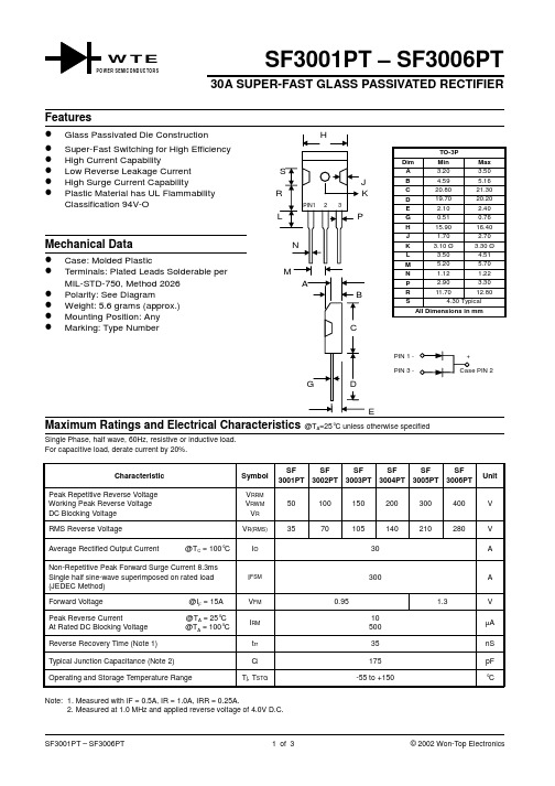
SF3001PT – SF3006PT30A SUPER-FAST GLASS PASSIVATED RECTIFIERSingle Phase, half wave, 60Hz, resistive or inductive load.For capacitive load, derate current by 20%.CharacteristicSymbol SF 3001PT SF 3002PT SF 3003PT SF 3004PT SF 3005PT SF 3006PT UnitPeak Repetitive Reverse Voltage Working Peak Reverse Voltage DC Blocking Voltage V RRMV RWM V R 50100150200300400V RMS Reverse VoltageV R(RMS)3570105140210280V Average Rectified Output Current @T C = 100°C I O30ANon-Repetitive Peak Forward Surge Current 8.3ms Single half sine-wave superimposed on rated load (JEDEC Method)I FSM 300A Forward Voltage @I F = 15A V FM 0.951.3V Peak Reverse Current @T A = 25°C At Rated DC Blocking Voltage @T A = 100°C I RM 10500µA Reverse Recovery Time (Note 1)t rr 35nS Typical Junction Capacitance (Note 2)C j 175pF Operating and Storage Temperature RangeT j , T STG-55 to +150°CNote: 1. Measured with IF = 0.5A, IR = 1.0A, IRR = 0.25A.2. Measured at 1.0 MHz and applied reverse voltage of 4.0V D.C.W T EWER SEMICONDUCTORS601201800240300360110100I ,P E A K F O R W A R D S U R G E C U R R E N T (A )F S M NUMBER OF CYCLES AT 60HzFig.3Max Non-Repetitive10100400V ,REVERSE VOLTAGE (V)Junction CapacitanceR C ,C A P A C I T A N C E (p F )j 0.010.11.0101004080120I ,I N S T A N T A N E O U S R E V E R S E C U R R E N T (m A )R PERCENT OF RATED PEAK REVERSE VOLTAGE (%)Fig.5Typical Reverse Characteristics0612182430050100150I ,A V E R A G E F O R W A R D C U R R E N T (A )(A V )T ,CASE TEMPERATURE (C)Fig.1Forward Current Derating CurveC °0.11.0101000.20.61.01.4I ,I N S T A N T A N E O U S F O R W A R D C U R R E N T (A )F V ,INSTANTANEOUS FORWARD VOLTAGE (V)Fig.2Typical Forward CharacteristicsFORDERING INFORMATIONProduct No.Package TypeShipping QuantitySF3001PT TO-3P 30 Units/Tube SF3002PT TO-3P 30 Units/Tube SF3003PT TO-3P 30 Units/Tube SF3004PT TO-3P 30 Units/Tube SF3005PT TO-3P 30 Units/Tube SF3006PTTO-3P30 Units/TubeShipping quantity given is for minimum packing quantity only. For minimum orderquantity, please consult the Sales Department.Won-Top Electronics Co., Ltd (WTE) has checked all information carefully and believes it to be correct and accurate. However, WTE cannot assume any responsibility for inaccuracies. Furthermore, this information does not give the purchaser of semiconductor devices any license under patent rights to manufacturer. WTE reserves the right to change any or all information herein without further notice.WARNING : DO NOT USE IN LIFE SUPPORT EQUIPMENT. WTE power semiconductor products are not authorized for use as critical components in life support devices or systems without the express written approval.We power your everyday.Won-Top Electronics Co., Ltd.No. 44 Yu Kang North 3rd Road, Chine Chen Dist., Kaohsiung, Taiwan Phone: 886-7-822-5408 or 886-7-822-5410Fax: 886-7-822-5417Email: sales@Internet: 。

thx202h工作原理
THX202H是一个数字音频放大器芯片,它的工作原理涉及到数
字信号处理和功率放大两个方面。
首先,THX202H通过数字信号处理部分接收来自音频源的数字
信号。
这些数字信号经过解码和处理,以确保音频信号的高保真度
和低失真度。
THX202H采用先进的数字信号处理技术,能够对音频
信号进行精确的调节和优化,以提供清晰、逼真的声音效果。
其次,经过数字信号处理的音频信号被送入功率放大器部分。
THX202H采用高效的功率放大技术,能够将低电压的数字信号转换
为足够驱动扬声器的高功率输出。
这种功率放大器设计能够确保音
频信号的高保真度的同时,提供足够的音量和动态范围。
除此之外,THX202H还可能包括一些保护电路,如过热保护、
短路保护等,以确保芯片和连接的设备在工作过程中不会受到损坏。
总的来说,THX202H的工作原理主要涉及到数字信号处理和功
率放大两个方面,通过先进的技术和设计,它能够提供高保真度、
低失真度的音频放大效果。

高速运算放大器——型号列表 制造商 产品类别 产品型号产品描述 ADI 公司 电压反馈高速运放AD812AR 低功耗电流反馈双运放 SN10501D 低失真,满幅输出高速运算放大器 SN10501DBVT低失真,满幅输出高速运算放大器 THS4120CD3.3V,100MHZ 全差分满幅度输出运放 THS4120ID3.3V,100MHz,43V/μs,全差分CMOS 运放(带关断功能) THS4121CD100MHZ 全差分满幅度输出运放 THS4130ID完全差分输入输出低噪声运放(带关断功能) THS4150ID完全差分输入输出高限斜率运放(带关断功能) THS4271D高速、高转换率、低失真差分运放 THS4275D高速、高转换率、低失真差分运放(关断功能) THS4500CD高速全差分运放 THS4501CD高速全差分运放 THS4505D宽带宽低失真全差分运放 TI 差分高速运放 THS7530PWP 高速全差分运放OPA2658U 双路,高速,低功耗,宽带,电流反馈型运放 OPA2677U 双路,宽带,高输出电流运放OPA2681U 双路,超高速,宽带,带关断功能,电流反馈型运放 OPA2684ID 双路,低功耗,电流反馈型运放OPA2691ID 双路,宽带,电流反馈运放带关断功能 OPA4658U 低功耗电流反馈运放OPA4684ID 四路,低功耗,电流反馈型运放OPA603AP 高速电流反馈放大器OPA658P 宽带,低功耗,电流反馈型运放OPA658U 宽带,低功耗,电流反馈型运放OPA685U 超带宽,电流反馈运放,带关断功能 OPA691ID 宽带,带关断功能,电流反馈型运放 THS3001CD 超高速,电流反馈运放THS3001ID 超高速,电流反馈运放THS3061D 单通道高速电流反馈运放THS3062D 双通道高速电流反馈运放THS3091D 单通道高速电流反馈运放THS3092D 双通道高速电流反馈运放THS3110CD 低噪声单通道高速运放THS3115ID 高输出电流运放电流反馈高速运放 THS3202D 2G 低失真电流反馈运放OPA2652U 双路,700MHZ,电压反馈运放TI 公司 电压反馈高速运放 OPA2690I-14D双路,高速,宽带,电压反馈型运放OPA2690ID双路,高速,宽带,电压反馈型运放 OPA2822U双路,低噪声,高速运放 OPA4650U四路, 高速,宽带,低功耗,电压反馈型运放 OPA642U高速运放 OPA650U高速,宽带,低功耗,电压反馈型运放 OPA657U1.6GHz,低噪音, FET 输入,高速,电压反馈型运放 OPA687U超高速,宽带,低功耗带关断功能电压反馈型运放 OPA690ID宽带,电压反馈运放带关断功能 OPA690IDBVT宽带,电压反馈运放带关断功能 SN10502D高速轨对轨视频运放 SN10503D低失真高速轨对轨运放 THS4001CD电压反馈放大器 THS4001ID电压反馈放大器 THS4011ID290MHz 低失真高速电压反馈单通道放大器 THS4021CD电压反馈放大器 THS4022ID电压反馈放大器 THS4052CD电压反馈放大器 THS4062CD180MHz 高速双放大器 THS4082CD175-MHz 双路低功耗电压反馈运放 THS4211D高速,极低失真电压反馈运放 THS4221D低噪声高速运放 THS4221DGN低噪声高速运放 THS4225D低噪声高速运放 THS4225DGN低噪声高速运放 EL4543IU 带共模同步译码功能的三通道差分双绞线驱动器 EL5171IS单通道,250MHz 差分双绞线驱动器 EL5172IS单通道,250MHz 差分线性接收器,单输出运算放大器 EL5172IY单通道,250MHz 差分线性接收器,单输出运算放大器 EL5410CS四路 30MHz 满幅输入输出运放 INTERSIL 公司 差分高速运放 EL9110IU差分接收器(5 pole),和均衡器 LT6230-10 LT1226LT1993-2LT1886LT6553LT6554LT1222LT1397LT1396LT1395LINEAR公司 高速放大器 LT1819LT1192LT1194LT1807LT1806LT1399LT1399HV LT6402-20 LT1398LT1254LT1253LT1252LT1815LT1817LT1816LT6231LT6232LT6230LT1739LT6211LT1794LT6300LT6210LT1809LT1810LT1203LT1225LT1205LT1221LT1227LT1259LT1260LT6551LT6550LT1814LT6206LT1813HV LT1229LT1228LT1230LT6205LT1223LT6207 LT1812 LT1204 LT1469 LT1191 LT1468 LT1805 LT1803 LT1193 LT1801 LT1800 LT1802 LT1804 LT1363 LT1994 LT1365 LT1206 LT1207 LT1126 LT1127 LT1795 LT1497 LT1360 LT1187 ,LT1364 LT1195 LT1362 LT1361 LT1190 LT1209 LT1632 LT1208 LT1633 LT1224 LT1220 LT1630 LT1631 LT1213 LT1214 LT1358LT1359 LT1216 LT1215 LTC6241 LTC6242 LT1355 LT1354 LT1356 LT1797。
PRODUCTION DATA information is current as of publication date. Products conform to specifications per the terms of Texas Instruments standard warranty. Production processing does not necessarily include testing of all parameters.元器件交易网IMPORTANT NOTICETexas Instruments and its subsidiaries (TI) reserve the right to make changes to their products or to discontinueany product or service without notice, and advise customers to obtain the latest version of relevant informationto verify, before placing orders, that information being relied on is current and complete. All products are soldsubject to the terms and conditions of sale supplied at the time of order acknowledgement, including thosepertaining to warranty, patent infringement, and limitation of liability.TI warrants performance of its semiconductor products to the specifications applicable at the time of sale inaccordance with TI’s standard warranty. Testing and other quality control techniques are utilized to the extentTI deems necessary to support this warranty. Specific testing of all parameters of each device is not necessarilyperformed, except those mandated by government requirements.CERTAIN APPLICATIONS USING SEMICONDUCTOR PRODUCTS MAY INVOLVE POTENTIAL RISKS OFDEATH, PERSONAL INJURY, OR SEVERE PROPERTY OR ENVIRONMENTAL DAMAGE (“CRITICALAPPLICATIONS”). TI SEMICONDUCTOR PRODUCTS ARE NOT DESIGNED, AUTHORIZED, ORWARRANTED TO BE SUITABLE FOR USE IN LIFE-SUPPORT DEVICES OR SYSTEMS OR OTHERCRITICAL APPLICATIONS. INCLUSION OF TI PRODUCTS IN SUCH APPLICATIONS IS UNDERSTOOD TOBE FULLY AT THE CUSTOMER’S RISK.In order to minimize risks associated with the customer’s applications, adequate design and operatingsafeguards must be provided by the customer to minimize inherent or procedural hazards.TI assumes no liability for applications assistance or customer product design. TI does not warrant or representthat any license, either express or implied, is granted under any patent right, copyright, mask work right, or otherintellectual property right of TI covering or relating to any combination, machine, or process in which suchsemiconductor products or services might be or are used. TI’s publication of information regarding any thirdparty’s products or services does not constitute TI’s approval, warranty or endorsement thereof.Copyright © 1999, Texas Instruments Incorporated。
概述:3001是一款非隔离线性LED恒流驱动芯片,可以实现高精度的LED恒流驱动。
3001可通过外置检流电阻调节输出电流。
3001因其特殊的恒流控制机制,芯片无需变压器,即可实现LED的恒流驱动,芯片本身具有过温保护功能,提高系统可靠性。
特性:◆内置高压启动供电◆±4%LED输出电流精度◆输出电流外置可调:5mA~60mA◆内部集成450V功率管◆无需变压器◆过温调节功能◆外围线路简单,元器件少◆产品可直接焊在铝基板上◆系统应用无EMI问题应用范围:◆LED吸顶灯◆LED球泡灯◆T5/T8系列LED日光灯管◆其他LED照明最大额定值:封装耗散等级(注1):注1:超出“最大额定值”可能损毁器件。
在极限条件下工作,器件特性将得不到保证,长期运行还可能会影响可靠性。
耗散功率(注2):注2:“耗散功率”是在25℃条件下,基于85mm*85mm厚度为1mm的铝基板测试;超出“最大额定值”不保证其特性。
电气特性(T TYP=25℃):项目符号测试条件最小值典型值最大值单位DN输入电压V DN_MIN IDN=30mA 6.5VDN耐压V DN450V静态电流I DD250uACS端口电压V CS VDN=10V300mV过温调节T REG140℃输出电流I OUT560mA典型应用:推荐工作范围:交流输入电压使用范围在200V至240V。
使用说明:3001作为一款LED恒流驱动控制芯片,芯片内部集成了LED恒流控制电路模块,温度调节模块。
芯片可通过外置的RCS检流电阻实现输出电流5mA~60mA 变化,DN端口的最低工作电压为6.5V。
通过外部的CS口电阻R CS来精确设定LED的电流,输出电流的计算公式如下:其中I LED是产品的输出电流,VCS是CS端口的检测电压,R CS是检流电阻。
3001具有过温调节功能。
在产品温度过高时,芯片内部将会逐渐减小检测电压VCS,进而减小输出电流,减小芯片的温升,保护芯片和系统的安全。
宽带直流放大器摘要:本系统以ADuC845单片机为控制核心,辅以前级放大电路,功率放大电路以及液晶显示、键盘输入等外围电路,实现了宽带直流放大功能。
本系统前级放大部分由OPA365、OPA695、THS3001芯片级联组成,通过调节电位器实现电压增益在0~60dB范围内连续可调;单片机数据处理、控制和显示模块实现可预置并显示电压增益;功率放大电路由两级三极管进行直流耦合和发射结直流负反馈构建,本设计采用高级压控增益器件,进行合理的级联和阻抗匹配高了稳定性与可控性。
关键字:宽带直流放大器;单片机;增益可调;THS3001;Abstract:Keywords:1.系统方案1.1系统总体设计思路根据设计要求,本系统由前级放大部分、单片机程控部分、功率放大部分和输入显示部分组成。
充分利用模拟的优点,发挥其优势,采用单片机预置和控制放大器增益的方法,大大提高了系统的精度和可控性。
首先由放大部分对输入的正弦信号进行电压增益连续可调的放大处理,然后经过程控部分,通过单片机完成对程控部分的电压衰减来实现电压增益的预置,再由液晶显示相关参数的设置。
系统结构框图如图1所示:图1 系统结构框图根据题目要求,分以下几个部分进行方案论证与选择1.2 可调增益放大部分方案一:可由三极管搭建的放大电路实现,为了满足增益大于60dB的要求必须采用多级放大,对电路输出用二极管检波产生反馈电压调节前级电路实现自动增益的调节。
本方案采用大量分离元件,电路比较复杂,工作点难于调整,,尤其增益的定量调节非常困难。
此外,由于采用多级放大,电路稳定性差,容易产生自激现象。
方案二:采用集成运放芯片,用集成运放芯片搭建放大电路可以很好的克服模拟电路的缺点。
本系统采用由OPA365、OPA695和THS3001三级级联组成的放大电路,可实现电压增益的连续调节。
OPA365检测微弱信号并作为精密运算放大器,在放大小信号时只有很小的输入失调电压,并能很好的抑制高频噪声。
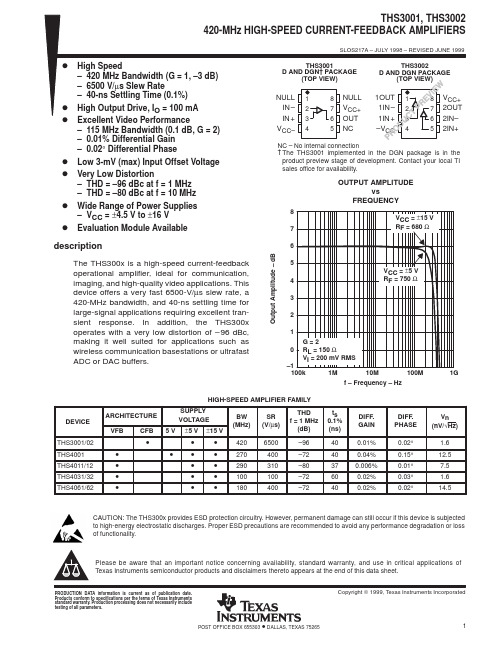
超高速运放THS3001
随着通信和多媒体技术的迅猛发展,对高速集成电路的要求不断提高,
TH3001 就是美国德州仪器公司为适就这种形势而生产的超高速运算放大器,
它采用电流模技术制造,是一种电流负反馈运算放大器,它以其独特的性能赢
得了电子工程师的极大关注。
THS3001 除了具有目前最高的转换速率外,还可使用±15V电源,其输出信号幅度可达±12V,它的推出为电子工程为员提供了
极大方便。
THS3001 具有高达6500V/μs的转换速率,420MHz 的-3dB 带度和良好的带内平坦度,在110MHz 时,增益仅下降0.1dB;大信号应用时具有40ns 的建立时间;差分增益误差小于0.01%,差分相位误差小于0.02%;非线性失真小于- 96dB;电源电压可在±4.5~±15V之间选择,单电源工作时可在9~30V 之间使用;输出电压最大可达±12V。
THS3001 的最大共模输入电压可接近±Vcc,最
大差模输入电压可达±6V,最大输出电源达100mA。
THS3001 以其上述优异的技术指标被广泛应用于图象处理系统、通信系统、高清晰电视电路、高速ADC 或DAC 缓冲器、高频脉冲放大和高质量的视频放
大等方面。
它的超高速特性和大信号输出范围是一般高速运放不能比拟的。
THS3001 采用表面安装8 引脚封装形式,各引脚排列如图1 所示。
图2 所示是THS3001 的频响曲线。
HTS3001 在脉冲大信号输入时的响应曲线如图3
所示。
在使用THS3001 时有以下几点需要特别指出:
(1)THS3001 的最大闭环增益为5 时能表现出最好的性能。
(2)THS3001 工作在反相放大状态时的频响比同相放大状态时好。
(3)负反馈电阻RF 对频响和波形失真有较大影响,因此应使用表1 所推存的值。
表1 最佳频响的RF 选择。