蓝牙F天线PCB设计 Pattern_Antenna
- 格式:pdf
- 大小:23.94 KB
- 文档页数:1

2.4GHZ 2.4GHZ倒F及弯曲线 及弯曲线PCB蓝牙 PCB蓝牙天线 蓝牙天线设计指导 设计指导1Contents1 2 3 4 5 6 7 8 9 Introduction .................................................................................................................................................... 3 Inverted-F Antenna ........................................................................................................................................ 4 Meander Line Antenna................................................................................................................................... 5 Real Designs .................................................................................................................................................. 6 Proximity to Metal Objects ............................................................................................................................ 7 Proximity to Dielectric Materials................................................................................................................... 8 Network Analyser........................................................................................................................................... 9 Final Tuning.................................................................................................................................................. 10 Conclusion ................................................................................................................................................... 12Terms and Definitions ........................................................................................................................................ 13 Document History ............................................................................................................................................... 14List of Figures Figure 2.1: Inv erted-F Antenna ............................................................................................................................... 4 Figure 3.1: Meander Line Antenna .......................................................................................................................... 5 Figure 3.2: Input Impedance of Two Meander Line Antennas................................................................................. 5 Figure 4.1: Approximate Dimensions of Inverted-F Antenna................................................................................... 6 Figure 4.2: Approximate Dimensions of Meander Line Antenna ............................................................................. 6 Figure 7.1: Preparation Before Measurement ......................................................................................................... 9 Figure 7.2: Assembled System Ready to Measure ................................................................................................. 9 Figure 8.1: Locating Product in Far Field of Antenna............................................................................................ 10 Figure 8.2: Final Tuning Procedure....................................................................................................................... 11第 2 页 共 13 页1IntroductionThis document outlines two ty pes of Printed Circuit Board (PCB) antennas used by CSR, which can be used with 2.4GHz radios. ■ Inverted-F ■ Meander Line In addition, this document discusses the effect of placing metallic or dielectric materials near an antenna.第 3 页 共 13 页2Inverted-F AntennaQuarterwaveInput OutputFigure 2.1: Inverted-F Antenna The inv erted-F is a quarterwav e antenna. It is bent into an L-shape. The shorter side is connected to earth. The longer side is left open-circuit at the end. The f eed point is located somewhere between the earth end and the open end. The resulting structure resembles the letter F and possesses the properties of both a loop antenna due to the circulating current from the f eed point to ground and a whip antenna due to the open circuited straight section. In the PCB v ersion, the antenna is printed on the top layer and a ground plane is placed near the antenna on the top lay er. There must not be a ground plane underneath the antenna. The aim is to make the quarterwav e section resonate at the midband frequency (which is 2441MHz f or 2.4GHz ISM radios). The f eed point (which is the input/output connection) is connected to the L-Shape at the point corresponding to 50∧ . Experiment with measurement to determine the correct location for the feed point and length of this antenna.第 4 页 共 13 页3Meander Line AntennaS Ground Plane Input Output第 5 页 共 13 页Figure 3.1: Meander Line Antenna The length of the meander line antenna is difficult to predict. It is usually a bit longer than a quarterwav e but dependent on its exact geometry and proximity to the ground plane.Note:In Figure 3.1 the ground plane is shown in black. S is the distance from the ground plane. See Figure 4.2 for approximate dimensions. This ty pe of antenna is alway s a PCB version. The antenna is printed on the top lay er and a ground plane is placed near the antenna on the top lay er. There must be no ground plane underneath the radiating section of the antenna.Smith ChartABFigure 3.2: Input Impedance of Two Meander Line Antennas The real part of the impedance of this antenna is about 15∧ to 25∧ , depending on geometry and proximity to the ground plane. The impedance matching is done by adjusting the length of the antenna until the input impedance is at the unity conductance circle (when normalised to 50∧ ), in the top half of the Smith chart (Point A). A shunt capacitor is then connected between the antenna input and ground to match to 50∧ (Point B). Experimental measurement is used to determine the correct design.4Real Designs18.0mm13.5mm Width=0.8mm 6 .0mm 5 .0mm Not to scaleGround PlaneActual SizeFigure 4.1: Approximate Dimensions of Inverted-F Antenna第 6 页 共 13 页1.5mm1.0mm4.4mm Width=0.5mm 2.8mm 1.7mm Ground Plane Not to scale1.5pF CapacitorPlaced immediatel y after F eedpoint8 .0 mm FeedpointActual SizeFigure 4.2: Approximate Dimensions of Meander Line Antenna第 7 页 共 13 页5Proximity to Metal ObjectsCSR recommends keeping metal objects as far away f rom the antenna as possible. Keeping metallic objects out of the near field is usually adequate. Near Field = 2D / λ D is the largest dimension of the antenna. In the case of these antennas, this is approximately a quarterwav e (λ/4).Notes:2λ is the wav elength of the signal in f reespace. In the 2.4GHz ISM band, λ=122mm in freespace. Substituting D=λ/4 into the Near Field equation giv es Near Field = λ/8. Near Field = 122/8 mm = 15.25mm.第 8 页 共 13 页6Proximity to Dielectric MaterialsDielectric materials (like plastic or FR-4) detune an antenna by lowering its resonant frequency. The effect is not as serious as placing an antenna next to metal objects and can be corrected by reducing the length of the antenna. Theref ore, it is important to tune the antenna when it is in the product. This is done during the dev elopment of the product.第 9 页 共 13 页71. 2.Network AnalyserCut the PCB track (trace) just before the antenna matching network to isolate the f ilter and previous stages f rom the measurement. Connect a coaxial cable between the VNA and the PCB of the product. The coaxial cable must hav e f errite beads fitted over its outer sleeve. The f errite beads help to prev ent RF currents from f lowing on the outer sleeve, which would disturb the measurement. Solder the outer sleeve of the coaxial cable to the ground plane of the PCB as close as possible to the input of the antenna-matching network. Perf orm a One-Port calibration on the VNA with Open, Short, Loads connected at the end of the coaxial cable inside the product. Solder the inner conductor of the coaxial cable to the input of the antenna-matching network. Tune the antenna by adjusting the values of any “matching network” components, the feed point of the antenna or the length of the antenna until the S11 trace (display ed on the VNA) is at the centre of the Smith chart at the midband f requency 2441MHz. Repair the cut track by putting a small amount of solder over the cut.Use a v ector network analyser (VNA) to perform the initial tuning of the antenna:3. 4. 5.6.Figure 7.1: Preparation Before MeasurementVNAFerrite BeadsAntenna 2.4GHz RadioFigure 7.2: Assembled System Ready to Measure第 10 页 共 13 页8Final TuningAfter tuning the antenna using the VNA procedure, it is necessary to perf orm fine-tuning. This y ields a small improv ement and is the f inal optimisation of the antenna. It is best to perf orm this procedure in an anechoic chamber, but when this is not possible, an indoor or outdoor test range can be used. It is important to minimise radio signal reflections. Avoid metallic objects such as lab-benches, filing cabinets, lampposts and cars.Approximately 2m RX Antenna2.4GHz RadioSpectrum Analy serFigure 8.1: Locating Product in Far Field of Antenna第 11 页 共 13 页Connect omni directional receive antenna to a spectrum analyser Place fully assembled product approximatel y 2m away from receive antenna Put product into continuous transmitWatch power level of received signal on the specturm anal yser while moving receive antenna ±10cm in each of x,y,z planes to ensure it is not located in a null point. A sudden dip in received power indicates a null pointYesIs antenna located in a null point?No Rotate product around in the x,y,z planes until the maximum power level is observed on the spectrum anal yser. This ensures that the dominant polarisation mode of the antenna is measured.NoHas the maximum possible power level been observed on the spectrum anal yser?Yes Record power level observed on the spectrum analyser. Turn off product, disassemble it and make adjustments to length of antenna, feed point or matching componentsReassemble product and place it in the same location and orientation as beforeNoHas the maximum receive power been obtained?Yes End of procedure Repeat process on multiple devices to ensure results are repeatableFigure 8.2: Final Tuning Procedure第 12 页 共 13 页9ConclusionMetal objects should be kept at least 15.25mm away from the Inverted-F and Meander Line types of antennas in the 2.4GHz ISM band f or the antenna to work efficiently. If that is not possible, experiment to determine an acceptable trade-off between antenna performance and product size. Ev en by f ollowing these rules, antenna detuning can occur. This usually results in lowering the resonant frequency of the antenna. Correct this by reducing the length of the antennaTerms and DefinitionsISM PCB RF VNA Industrial, Scientific and Medical Printed Circuit Board Radio Frequency Vector Network Analyser第 13 页 共 13 页。

1. 简介
该文档是上海慧翰信息技术有限公司推出的蓝牙模块的硬件设计经验总结,适用于本公司的各个型号模块的硬件设计参考,敬请按型号区分要点。
如有何问题,请直接与本公司的工程师联系,您将会得到更详细的说明。
2. 天线设计
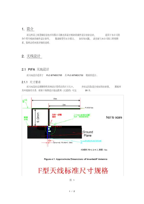
2.1 PIFA天线设计
该天线设计适用于FLC-BTMDC705及FLC-BTMDC732模块的设计。
2.1.1 尺寸要求
该天线是经过调频特性的理论计算得出的尺寸大小,并经过实际设计验证的经验值,跟板材及环境都有关系。
按如下规格设计最远距离(无遮挡)可达20米。
图 1
2.1.2 布线要求
首先,建议将天线按尺寸设计成元件封装,方便摆放及后续项目设计,并可以防止拖动造成尺寸大小变化,而来回修改。
其次,该天线是与地线连接的,天线有效部分的周围及其下层(即
背面)不应用有元器、布线,更不应该铺铜,否则影响信号发射和接收,甚至无法正常工作。
第
三,该天线的接地点要求大面积接地,并多打过孔。
第四,该天线要求设计在PCB板的板边,尽量朝前面板,并要求周围避开铁质结构件。
2.1.3 板材要求
板材请选用:FR4,介电常数为 4.2
2.2 外引天线设计
请断开PIFA天线的连接电路,并用10pF的电容连接外引天线。
外引天线的线材要求采用
50欧高频屏敝电缆,并在尾部去掉3CM长的屏敝层。
线头的中间信号线焊接在天线输出端,而
屏敝铁线也应该焊在就近地线位置,该天线尾部应放置于前面板靠前位置或者引至铁壳之外。
Freescale Semiconductor Application Note AN2731Rev. 1.2, 11/20041Introduction Good antenna design is the most critical factor in obtaining good range and stable throughput in a wireless application. This is especially true in low power and compact designs, where antenna space is less than optimal. However, several compact, cost efficient, and very effective options exist for implementing integrated antennas.To obtain the desired performance, it is required thatusers have at least a basic knowledge about howantennas function, and the design parameters involved.These parameters include selecting the correct antenna,antenna tuning, matching, gain/loss, and knowing therequired radiation pattern.This note will help users understand antenna basics, andaid in selecting the right antenna solution for theirapplication.Compact Integrated Antennas Designs and Applications for the MC13191/92/93Contents1Introduction . . . . . . . . . . . . . . . . . . . . . . . . . . 12Antenna Terms . . . . . . . . . . . . . . . . . . . . . . . . 23Basic Antenna Theory . . . . . . . . . . . . . . . . . . 24Impedance Matching . . . . . . . . . . . . . . . . . . . 65Miniaturization Trade-offs . . . . . . . . . . . . . . 136Potential Issues . . . . . . . . . . . . . . . . . . . . . . 147Recommended Antenna Designs . . . . . . . . 148Design Examples . . . . . . . . . . . . . . . . . . . . . 16Antenna Terms2Antenna TermsAntenna Gain A measure of how well the antenna radiates the RF power in a given direction, compared to a reference antenna, such as a dipole or an isotropic radiator. The gainis usually measured in dB’s. A negative number means that the antenna in questionradiates less than the reference antenna, a positive number means that the antennaradiates more.Decibel (dB) A logarithmic scale used to represent power gain or loss in an RF circuit. 3 dB isa doubling of the power, -3 dB is half the power. -6 dB represents half the voltageor current, and quarter the power.Radiation Resistance The part of antenna’s impedance which produces radiated power. The measured impedance of an antenna is comprised of radiation resistance and loss.3Basic Antenna TheoryEvery structure carrying RF current generates an electromagnetic field and can radiate RF power to some extent and likewise an external RF field can introduce currents in the structure. This means that theoretically any metallic structure can be used as an antenna. However, some structures are more efficient in radiating and receiving RF power than others. The following set of examples explains this concept. Transmission lines (striplines, coaxial lines etc.) are designed to transport RF power with as little radiation loss as possible because these structures are designed to contain the electromagnetic fields. To obtain any appreciable radiation from such a structure, requires excessively high RF currents which causes low efficiency due to high losses. Likewise, the ability to introduce RF currents into the structure is of importance, described by the feed point impedance. If the feed point impedance is very high, low, and/or highly complex, it is difficult to introduce RF current with good efficiency.The antenna structure should be of reasonable size compared to the wavelength of the RF field. A natural size is half a wavelength, which corresponds to approximately 6 cm at the 2.4 GHz ISM band. This size is effective because when fed with RF power at the center point, the structure is resonant at the half wave frequency. Reducing the size below 6cm tends to make the antenna less visible to the RF field and not resonant which causes low efficiency. Not all structures make an efficient antenna.Numerous structures have been devised that provide good efficiency and impedance match, but most of these are derived from a few basic structures. A short description of these basic antennas, and some good advice on how to implement these with success is provided later in this note.This note does not include complicated formulas concerning antenna theory because it is beyond the scope of this note. The intention of this note is to provide basic information about how antennas work, which should allow users to achieve reasonable performance with a minimum number of attempts.If users are interested in performing complex calculations and antenna simulations, they should consult the abundant and widely available literature concerning antenna theory and design. Note that simply copying an existing design does not necessarily ensure reasonable performance. A lot of external factors affect antenna tuning, gain, radiation patterns, etc. An antenna tuned for one set of environmental factors may not perform at all if put into a new environment, and may require a lot of tuning to achieve even reasonable performance.Basic Antenna Theory 3.1Basic Antenna Variations3.1.1 3.1.1 Dipole AntennaThe dipole is one of the most basic antennas. The dipole is a straight piece of wire cut in the center and fed with a balanced generator or transmission line. As previously stated, this structure is resonant, ornon-reactive, at the frequency where the conductor length is 1/2 wavelength. For the ISM band, this length is approximately 6 cm or about 2 ½ inches. At this length, the dipole shows resonance, the feed impedance is resistive, and is close to 73 Ohms. This also holds true for a very thin wire in free space.Figure1. Basic DipoleA practical dipole of some thickness, loaded with different dielectric materials (PCB etc.), and perhaps relatively close to ground, shows resonance at a slightly shorter length than calculated, and the radiation resistance drops somewhat. For dipoles not too close to ground, the shorting factor is typically in the range of 5-20%, the shorter being more heavily dielectric loaded, and radiation resistance is in the range of 35-65 Ohms.This dipole setup exhibits a relatively good match to a 50 Ohm generator, but the feed is differential. A small ceramic balun can be used for single-ended feed. The bandwidth is typically 2-5%, depending on the return loss required. The radiation pattern in free space is doughnut-shaped, with pronounced dips along the direction of the wires.To fill out these dips, the outer ends of the antenna can be bent at a 45 degree angle. Several configurations are possible, including the “broken arrow” shape. Any materials close to the antenna can distort the radiation pattern.Basic Antenna TheoryFigure2. Dipole Shapes to Improve Omnidirectional CharacteristicsTo reduce the size of the dipole, several options exist:•Replacing some of the wire length with loading coils•Bending the dipole ends back on the dipole•Folding the dipole into a meander pattern•Hairpin or coil loading of the center•Capacitive loading of the dipole endsBasic Antenna TheoryFigure3. Dipole Loading ExamplesIn general, the smaller the antenna, the lower the radiation resistance and the lower the efficiency. The antenna should also be removed somewhat from the ground plane, preferably at least ¼ wavelength (3 cm) but not less than 1 cm. Sometimes a loading technique is employed where the dipole ends are bent close to the ground plane, or even loaded with small capacitors to ground. This technique shorts the dipole considerably but causes heavy RF currents to flow in the ground plane, resulting in low efficiency. Often some of the other loading techniques result in better performance.Impedance Matching4Impedance MatchingFor heavily loaded antennas and antennas close to ground, the radiation resistance may deviate considerably from 50 Ohms which causes a poor match. An Inductive/Capacitive (LC) matching network may be employed, but better efficiency is possible by raising the feed impedance.These techniques may also be employed if an impedance higher than 50 Ohm is required.The current and voltage distribution on a dipole is such that the impedance is low in the center and raises towards the ends. By tapering the dipole at some distance from the center, an appropriate match can be found. The tapering may take the form of Gamma, Delta or Capacitive tapping as shown in Figure 4. This allows for matching impedances from 2 up to 300 Ohms. Some loading may be required to take out the reactance introduced by the tapering, or the antenna could be slightly offset tuned to compensate for the added reactive component.Another approach is using the folded dipole. This is where two parallel wires are placed closely together. Due to the tight coupling, the current distribution is approximately proportional to the surface area of each wire. This means that in two equal wires, the current in the feeding wire is approximately half the value of the wires together. Half the current at the same power means twice the voltage, or four times the impedance of 73 Ohms (292 Ohms). In practice, the impedance is somewhat lower, as in the normal dipole case. however, by changing the relative wire diameter, or even introducing several wires, it is possible to tune the impedance from less than 100 Ohms to several hundred Ohms.Impedance MatchingFigure5. The Folded DipoleAll the different dipole types, loading techniques, and feeding networks total up to an enormous amount of possible combinations, each with its own advantages and disadvantages. Selection of the correct design for your application is best found using case-by-case assessment.4.1Monopole AntennasIf one part of a dipole antenna is removed and replaced by an infinite ground plane, the remaining half of the dipole “mirrors” itself in the ground plane, much in the same way that one sees their own reflection in water.For all practical purposes, the monopole behaves as a “half” dipole. That is, it has the same doughnut shaped radiation pattern, the radiation resistance is half that of the dipole (37 Ohm), it can be bend and be folded like the dipole, and the same loading and feeding techniques can be applied.However, one very important difference remains in that the antenna feed point is not balanced, but single ended. Because of this and because most RF circuits are of the unbalanced type, this antenna type has been immensely popular and a lot of variations of the monopole theme exist, most designed to match 50 Ohms.FigureIt is important to note that the “whip” is only half the antenna and that the remainder is made up of the ground plane, or counter weight, as it is sometimes called. In a practical application, the ground plane is often made up of the remainder of the PCB (ground and supply planes, traces, and components).Impedance MatchingThe ground plane should be a reasonably sized area compared to the antenna, and should be reasonably continuous. If a monopole is used on a very small PCB, perhaps even with only a small area of copper, efficiency suffers, and the antenna is difficult to tune. Components and tracks introduce additional losses and affect the feed point impedance.As for the dipole, resonance is obtained at a length slightly shorter than one quarter wavelength, typically 5-15% shorter. Typical lengths are slightly more than an inch or two or 3 to 5 cm. The radiation resistance is caused by bending the antenna, and like the dipole, the marked dip in the radiation pattern can be eliminated. By bending the antenna closer to ground, the radiation resistance and efficiency drops, so the antenna should not be placed too close to ground. Like the dipole, the monopole can also be folded and bent around corners, if board space requires this, or it can be loaded with series coils.Of the many variations that exist, the following sections highlight the most common.4.1.1PCB Whip, Quarter Wave Monopole, or Quarter WaveIf board space allows, a full-size quarter wave antenna is quite efficient and often provides a reasonable match to a 50 Ohm system. Slight folding or bending of the ends has negligible impact on performance.4.1.2Open Stub, Tilted WhipIf the monopole is bent and traced along the ground plane, it will be more compact and the null in the radiation pattern is partly eliminated. The antenna should not bee too close to ground, preferably not closer than 1/10 wavelength (1 cm), or efficiency suffers too much. At this close spacing, the radiation resistance is so low (in the order of 10 Ohms) that a matching network is usually needed. If the monopole is very close to ground, it resembles a transmission line, with little or no radiation at all.4.1.3The F-AntennaThe F-antenna can be thought of as a tilted whip, where impedance matching is done by tapping the antenna at the appropriate impedance point. Because this antenna is reasonably compact, has an omnidirectional radiation pattern, good efficiency, and is very simple, it is used extensively in applications, including the mobile communications business. It should be noted that the currents in the ground leg are high, and that a good sized ground plane is necessary to provide good efficiency.Impedance Matching 4.1.4The HelixIf a quarter wavelength is coiled up, a very compact antenna can be made which still has reasonable efficiency. Some experimentation may be required to find resonance, because the length of the wire is not exactly related to a quarter wavelength. This type of antenna is very popular at lower frequencies.4.1.5The SpiralA spiral antenna, with the windings in one plane like a pancake, is well suited to be implemented on a PCB. Performance is similar to the helix.4.1.6The Meander AntennaThe meander antenna or meander pattern, is an antenna with the wire folded back and forth where resonance is found in a much more compact structure than can otherwise be obtained.The meander, spiral, and helix antennas are similar in that resonance is obtained in a compact space by compressing the wire in different ways. In all three cases, the radiation resistance, bandwidth, and efficiency drops off as size is decreased, and tuning becomes increasingly critical. Impedance matching can be implemented by tapping, as in the F-antenna. The meander and helix antenna, or a combination of these two, are easily implemented in a PCB, and many chip antennas are based on these types of antenna.Figure8. Meander Pattern (Tapped for Impedance Match)Impedance Matching4.2Loop AntennasLoop antennas can be divided in two groups:1.Half-wave antennas2.Full-wave antennasThe term wave refers to the approximate circumference of the loop.4.2.1Half-wave LoopThe half wave loop consists of a loop approximately half a wavelength in circumference, with a gap cut in the ring. It is very similar to a half-wave dipole that has been folded into a ring and much of the statements about the dipole apply to the half-wave loop. Because the ends are very close together, there exists some capacitive loading, and resonance is obtained at a somewhat smaller circumference than expected. The feedpoint impedance is also somewhat lower than the usual dipole, but all the usual feeding techniques can be applied to the half-wave loop. By increasing the capacitive loading across the gap, the loop can be made much smaller than a half wavelength. At heavy loading, the loop closely resembles a single winding LC tuned circuit. The actual shape of the loop is not critical. It can be shown that the efficiency is determined by the area enclosed by the loop. The half-wave loop is popular at lower frequencies. However, at higher frequencies, the tuning capacitance across the gap becomes very small and critical.4.2.2Full-wave LoopAs the name implies, the full wave loop is approximately one wavelength in circumference. Resonance is obtained when the loop is slightly longer than one wavelength, typically 10-15% longer. The full wave loop can be thought of as two end-connected dipoles. As is with the half-wave loop, the shape of the full wave loop is not critical, but efficiency is determined mainly by the enclosed area. The feed impedance is somewhat higher than the half-wave loop, typically around 120 Ohms.Loading can be done by inserting small coils or hairpins in the loop, thereby reducing the size. As is with the dipole and half-wave loop, there exists numerous ways for impedance matching, including gamma match and tapering across a loading coil or hairpin. The main advantage of the full-wave loop is that it does not have the air gap in the loop, which is very sensitive to load and PCB capacitance spread.Impedance Matching4.2.3Slot AntennasSlot antennas are used extensively in aircraft and radar applications. The basic slot antenna is a half wave slot cut in a conducting sheet of metal. The feed point is across the center of the slot and balanced. The feed impedance is high, typically several hundred Ohms. Because the slot antenna is the opposite of a dipole, that is, a non-conducting slot in a sheet of metal, as opposed to a conducting rod in free air, the slot antenna shows similarities to a dipole but also exhibits interesting differences as well.•The feed point is across the center, instead of in series, so the feed point impedance is high instead of low• E and H fields are switched, so that the polarity is opposite• A horizontal slot is equivalent to a vertical dipole•The slot antenna may be of interest, if the RF unit has to be placed in a metal enclosure, where the slot antenna could be made in the enclosure itself•If the slot antenna is cut in the center, a quarter wave slot antenna is created, which is equivalent to the monopole•Impedance matching can be done by tapping across the slot close to the shorted endThe slot antenna could be used if a metal enclosure is required, or if considerable board area is available. If the slot antennas are implemented in FR4 PCB, considerable dielectric loading occurs which causes the physical length to be shorter than expected.Impedance MatchingFigure10. Half-wave and Quarter-wave Slot Antennas4.2.4Patch AntennasPatch antennas are a group of antennas with a very low profile and are capable of working very close to a ground plane. However, they require a fair amount of board space. The radiation pattern may be omnidirectional or unidirectional. A few examples are shown, but design and tuning is not straightforward and is best left to an experienced antenna engineer. Some types of chip antennas that show unidirectional characteristics are of this design.4.2.5Chip AntennasMany different chip antennas are available commercially. To many, these antennas seem to work for no apparent reason, but careful investigation reveals that most of these antennas are based on a helix, meander, or patch design. To ensure proper operation it is very important to follow the manufacturer’s recommendations regarding footprint, ground areas, and mounting of the chip antenna. The “keep out” area around the antenna is especially important. Even following the recommendations does not always guarantee good performance due to de-tuning by nearby objects. It is to be expected that fine tuning of the antenna and/or a matching network is required to ensure satisfactory performance. Because chip antennas normally, but not always, use a ceramic material with higher dielectric constant and lower loss than the usual FR4, it is possible to make smaller antennas with reasonable efficiency.The efficiency is not exceptionally high, typically in the range of 10-50%, which corresponds to 3-10 dB loss (-3 to –10 dBi). The lower number being inferior products with high inherent losses. As already stated, buying a chip antenna does not guarantee good performance. However, they do provide the smallest antenna solution possible but the size reduction comes at a cost both in performance and pricing.If a slightly larger PCB area is available than is required by the chip antenna, and the “keep out” area can be allocated to a PCB antenna, it is possible to implement a PCB antenna with the same or better performance than a chip antenna but at a much reduced cost.4.2.6BalunsMany of the above antennas mentioned are single-ended and designed to have a feed point impedance close to 50 Ohms. To interface these antennas to a balanced output/input, a device called a balun is required. The balun converts a single ended input to a balanced output together with an optional impedance transformation. The output is differential. That is, the output voltage on each pin is of equal magnitude, but off opposite phase. The output impedance is normally stated differential. That is, measured betweenMiniaturization Trade-offs the two output pins. Because the balun is a discrete device, it is bidirectional. The balanced port can be both input or output.Several discrete circuits are available that perform as baluns. Most of them are sensitive to input and output loading and PCB layout which requires cumbersome fine tuning. And all of these require at least two chip inductors. In the 2.4 GHz band, small ceramic baluns exist which are easy to use and are less sensitive to the PCB layout. Standard output impedances are 50, 100 and 200 Ohms.The cost of a discrete balun is comparable to, or higher than, the ceramic balun, and the ceramic balun requires less board space. Therefore, the ceramic balun is recommended for most designs.To interface with the MC13192/92/93, the standard component 50–200 Ohm balun is recommended. A 50–400 Ohm device provides slightly better performance, but it is not an off-the-shelf device.5Miniaturization Trade-offsAs previously stated, reducing antenna size results in reduced performance. Some of the parameters that suffer are:•Reduced efficiency (or gain)•Shorter range•Smaller useful bandwidth•More critical tuning•Increased sensitivity to component and PCB spread•Increased sensitivity to external factorsAs stated, several performance factors deteriorate with miniaturization, but some antenna types tolerate miniaturization better than others. How much a given antenna can be reduced in size depends on the actual requirements for range, bandwidth, and repeatability. In general, an antenna can be reduced to half its natural size without much impact on performance. However, after a one half reduction, performance gets progressively worse as the radiation resistance drops off rapidly. As a rule, one half the antenna size equals one quarter the radiation resistance. As loading and antenna losses often increase with reduced size, it is clear that efficiency drops off quite rapidly.The amount of loss that can be tolerated depends on the range requirements. Bandwidth also decreases, which causes additional mismatch losses at the band ends. The bandwidth can be increased by resistive loading, but this often introduces even more loss than the mismatch loss. The low bandwidth combined with heavy loading requires a spread analysis to ensure adequate performance with variations in component values and PCB parameters. As shown by these facts, it is often better not to reduce antenna size too much, if board space allows. Even if range requirements do not require optimum antenna performance, production problems and spread are minimized. It is also best to keep some clearance between the antenna and nearby objects. Although the antenna may be retuned to compensate for the loading introduced by the surroundings, tuning becomes more critical, and the radiation pattern can be heavily distorted.Potential Issues6Potential IssuesNumerous things can go wrong with an antenna design. The following list provides a few do’s and don’t’s which may server as a good checklist in a final design. Many of these items seem obvious to the experienced antenna designer, but many of these issues are routinely encountered in practice. This is obviously not a complete list.•Never place ground plane or tracks underneath the antenna•Never place the antenna very close to metallic objects•Be careful about the wiring in the finalized product, not too close to the antenna• A monopole antenna should have a reasonable ground plane to be efficient•Do the final tuning in the end product, not in free air•Never install a chip antenna in a vastly different layout than the reference design, and expect it to work without tuning•Do not use a metallic enclosure or metallized plastic for the antenna•Test the plastic casing for high RF losses, preferably before production•Never do a cut and paste antenna design and expect it to work without testing•Never use low-Q loading components, or change manufacturer without retesting•Do not use very thin PCB tracks, the tracks should be fairly wide7Recommended Antenna DesignsTwo antenna designs are employed for the MC13192/93 hardware.1.Dipole (lowest cost implementation)2.F-antennaHowever, most antenna designs are intended to interface with the usual 50 Ohm industrial standard. This is certainly true for all chip antennas. For interfacing the MC13191/92/93 to a single-ended 50 Ohm antenna, it has been shown that the smallest and most cost-effective solution are two ceramic baluns and an RX/TX switch.The MC13192-EVB, which is included in the MC13193EVK-A00, provides an example of this setup. Users can omit the RX/TX switch and add two chip antennas, but in most cases the switch is less costly than another antenna. Any other 50 Ohm, single ended antenna design can be added if required. This includes among others the F-antenna, monopole, helical, and the usual commercially available chip antennas. The single-port, 50 Ohm solution has the added advantage that by adding a ceramic bandpass filter for improved performance is easy. For a very low cost, low bill of materials (BOM) count solution, users should consider interfacing the antenna(s) directly to MC13191/92/93, and integrate both antennas and matching components into the PCB.This setup does have some unique requirements, due to the input/output requirements of theMC13191/92/93. To achieve a good match to the MC13192/92/93, the antenna should include the following properties:•Balanced designRecommended Antenna Designs•Feedpoint impedance of 2-300 Ohm•Easily loaded to smaller size, with PCB or lumped loading•Provide a DC feed to the TX port•Easy to implement in FR-4 PCBOf the different antenna types, the following are especially suited to interface with the MC13191/MC13192:•Dipoles with gamma match, or folded dipoles•Half or quarter wave loops•The slot antenna may also prove useful in some casesBecause the MC13192/92/93 has separate RX and TX ports, two antennas will eliminate RX/TX switching. The two antennas should ideally be placed at least ¼ wavelength apart to reduce coupling, but due to the low power requirements, closer spacing can be allowed. The following list shows the results from testing with dipole antennas and shows the typical isolation. The values are empirical, and depend somewhat on the surrounding layout etc., but they should provide a reasonable indication of the isolation obtainable.•On each side of a PCB, on top of each other: – 3 to – 4 dB•Very close, on the same side of the PCB: – 6 dB•15 mm apart: – 10 dB•25 mm apart: – 13 dBFor the MC13192/92/93 to show optimum performance, at least 6 dB of TX to RX isolation is required or the ESD protection diodes in the RX input cause some TX power loss and perhaps also increased 3rd harmonic output. However, placing the RX and TX dipoles on top of each other, with only 3 dB of isolation results in the smallest design possible, and only reduces TX power a few dB, which is entirely acceptable in most cases. The RX side works well with any isolation available. When the antennas are very close, the coupling results in some interaction in the tuning of the two antennas. With just a few attempts, users should be able to optimize performance.。
电子产品世界设计应用无线技术esign & Application用于蓝牙和超宽带融合定位的倒F阵列天线设计*Design of the Inverted-F Array Antenna Used for Bluetooth and UWB Fusion Positioning林 斌 (厦门大学嘉庚学院,福建漳州363105)摘 要:本文针对高精度低功耗室内定位系统对天线的性能要求,将倒F天线结构、感应辐射阵列结构、渐变缝隙结构、分形光子晶体结构相结合,设计制作了用于蓝牙和超宽带融合定位的天线阵列。
这款天线在测试中具有蓝牙和UWB双频段工作能力,辐射性能和带宽性能优异,兼具全向天线和定向辐射能力。
使用本天线的室内定位系统,在进行米级定位时使用蓝牙频段,在进行厘米级高精度定位时使用超宽带频段,同时使用蓝牙频段低功耗地实时传输定位数据,可以兼具蓝牙室内定位系统和超宽带室内定位系统优点。
关键词:倒F天线结构;感应辐射阵列结构;渐变缝隙结构;分形光子晶体结构;室内定位天线室内定位系统是由多组定位信标依靠室内无线通信连接而成的新型高精度定位系统。
近年来,随着物联网技术和大数据技术的发展,室内定位的应用领域日益广泛。
蓝牙和超宽带(UWB )是目前最成熟的室内定位频段,他们各自有着自己的优缺点。
蓝牙室内定位系统成本低、功耗小、易于部署,但是有较大的传输延时,定位实时性不够好,定位精度只能达到米级。
超宽带室内定位系统探测距离远、传输速率高、定位实时性好,具有较高的多径分辨率,可以穿透各种材料,包括墙、木板、玻璃等,在室内复杂环境下可以实现厘米级的定位精度,但是功耗较大,单独使用会对定位信标的供电系统造成较大压力[1-5]。
将两种室内定位系统相结合,笔者团队设计出蓝牙和超宽带融合室内定位系统,使用超宽带通信频段进行定位信标探测,使用蓝牙通信频段进行定位数据传输,可以兼具蓝牙室内定位系统低成本、低功耗和超宽带室内定位系统探测距离远、传输速率高、定位实时性好、定位精度高的优点。
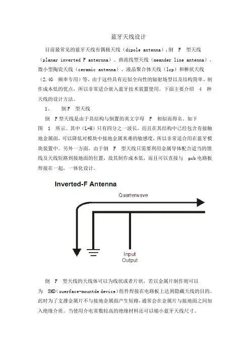
蓝牙天线设计目前最常见的蓝牙天线有偶极天线(dipole antenna),倒 F 型天线(planar inverted F anternna)、曲流线型天线(meander line antenna)、微小型陶瓷天线(ceramic antenna)、液晶聚合体天线(lcp)和棒状天线(2.4G 频率专用)等。
由于这些具有近似全向性的辐射场型以及结构简单、制作成本低的优点,所以非常适合嵌入蓝牙技术装置使用。
下面主要介绍 4 种天线的设计方法。
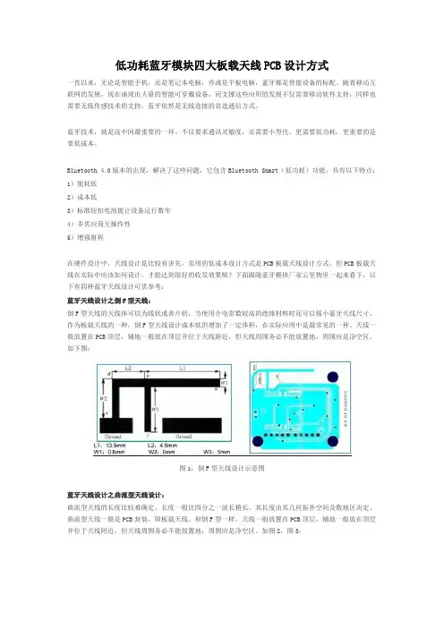
1、倒F 型天线倒F型天线是由于其结构与倒置的英文字母 F 相似而得名。
如下图 1 所示。
其中(L+H)只有四分之一波长,而且在其结构中已经包含有接触地金属面,可以降低对模块中接地金属米难的敏感度,所以非常适合用在蓝牙模块装置中。
另外一方面,由于倒 F 型天线只需要利用金属导体配合适当的馈线及天线短路到接地面的位置,故其制作成本低,而且可以直接与pcb电路板焊接在一起,一体化设计。
倒 F 型天线的天线体可以为线状或者片状,若以金属片制作则可以为SMD(suerface-mountde device)组件焊接在电路板上达到隐藏天线的目的。
此时为了支撑金属片不与接地金属面产生短路,通常会在金属片与接地面之间加入绝缘介质。
当使用介电常数较高的绝缘材料还可以缩小蓝牙天线尺寸。
图 2 给出了倒 F 型天线的pcb设计封装参数。
作为板载天线的一种,倒 F 型天线设计成本低但是增加了一定的体积,但是实际应用中是最长见一的一种。
倒 F 型天线是1/4 波长天线,除去其天线接入点外,其外轮廓为L 形状。
图 2 中蓝牙天线接入点与蓝牙芯片的天线引脚相连接,外轮廓L 型短边接地,天线接入点介于地和天线开放端之间。
板载F型天线一般放在pcb 顶层,铺地一般放在顶层并位于天线附近,但天线周围务必不能放置地,周围应是净空区。
图 3 给出了倒 F 型天线在PROTEL 中制作成板载天线的应用示范:2、曲流型天线曲流型天线的长度比较难确定。

蓝牙天线设计————————————————————————————————作者:————————————————————————————————日期:ﻩ蓝牙天线设计目前最常见的蓝牙天线有偶极天线(dipole antenna),倒F型天线(planar inverted F anternna)、曲流线型天线(meander line antenna)、微小型陶瓷天线(ceramic antenna)、液晶聚合体天线(lcp)和棒状天线(2.4G频率专用)等。
由于这些具有近似全向性的辐射场型以及结构简单、制作成本低的优点,所以非常适合嵌入蓝牙技术装置使用。
下面主要介绍 4 种天线的设计方法。
1、倒F 型天线倒F型天线是由于其结构与倒置的英文字母 F 相似而得名。
如下图 1 所示。
其中(L+H)只有四分之一波长,而且在其结构中已经包含有接触地金属面,可以降低对模块中接地金属米难的敏感度,所以非常适合用在蓝牙模块装置中。
另外一方面,由于倒 F 型天线只需要利用金属导体配合适当的馈线及天线短路到接地面的位置,故其制作成本低,而且可以直接与pcb电路板焊接在一起,一体化设计。
倒 F 型天线的天线体可以为线状或者片状,若以金属片制作则可以为SMD(suerface-mountde device)组件焊接在电路板上达到隐藏天线的目的。
此时为了支撑金属片不与接地金属面产生短路,通常会在金属片与接地面之间加入绝缘介质。
当使用介电常数较高的绝缘材料还可以缩小蓝牙天线尺寸。
图 2 给出了倒 F 型天线的pcb设计封装参数。
作为板载天线的一种,倒 F 型天线设计成本低但是增加了一定的体积,但是实际应用中是最长见一的一种。
倒F型天线是1/4 波长天线,除去其天线接入点外,其外轮廓为L 形状。
图 2 中蓝牙天线接入点与蓝牙芯片的天线引脚相连接,外轮廓L型短边接地,天线接入点介于地和天线开放端之间。
板载F型天线一般放在pcb 顶层,铺地一般放在顶层并位于天线附近,但天线周围务必不能放置地,周围应是净空区。
2.4 GHz Inverted F AntennaBy Audun AndersenKeywords• CC2400 • CC2420 • CC2430 • CC2431 • CC2500 • CC2510 • CC2511• CC2550 • CC2520 • CCZACC06 • PCB Antenna • 2.4 GHz• Inverted F Antenna1 IntroductionThis document describes a PCB antenna design that can be used with all 2.4 GHz transceivers and transmitters from Texas Instruments. Maximum gain is measured to be +3.3 dB and overall size requirements for this antenna are 25.7 x 7.5 mm. Thus, this is a compact, low cost and high performance antenna.Table of Contents KEYWORDS (1)1INTRODUCTION (1)2ABBREVIATIONS (2)3DESCRIPTION OF THE INVERTED F ANTENNA DESIGN (3)3.1I MPLEMENTATION OF THE I NVERTED F A NTENNA (3)4RESULTS (4)4.1R ADIATION P ATTERN (4)4.2R EFLECTION (11)4.3B ANDWIDTH (11)5CONCLUSION (12)6REFERENCES (13)7GENERAL INFORMATION (14)7.1D OCUMENT H ISTORY (14)2 AbbreviationsCCZACC06 Z-Accel ZigBee ProcessorEMModuleEvaluationAntennaFInvertedIFAMedicalScientific,ISMIndustrial,BoardCircuitPrintedPCB3 Description of the Inverted F Antenna DesignSince the impedance of the Inverted F Antenna is matched directly to 50 ohm no external matching components are needed.3.1 Implementation of the Inverted F AntennaIt is important to make an exact copy of the antenna dimensions to obtain optimum performance. The easiest approach to implement the antenna in a PCB CAD tool is to import the antenna layout from either a gerber or DXF file. Such files are included in CC2430DB reference design [1]. The gerber file is called “Inverted_F_Antenna.spl” and the DXF file is called “Inverted_F_Antenna.dxf”. If the antenna is implemented on a PCB that is wider than the antenna it is important to avoid placing components or having a ground plane close to the end points of the antenna. If the CAD tool being used doesn’t support import of gerber or DXF files, Figure 1 and Table 1 can be used.Figure 1. IFA DimensionsH1 5.70 mm W2 0.46 mmH2 0.74 mm L1 25.58 mmH3 1.29 mm L2 16.40 mmH4 2.21 mm L3 2.18 mmH5 0.66 mm L4 4.80 mmH6 1.21 mm L5 1.00 mmH7 0.80 mm L6 1.00 mmH8 1.80 mm L7 3.20 mmH9 0.61 mm L8 0.45 mmmmW1 1.21Table 1. IFA DimensionsSince there is no ground plane beneath the antenna, PCB thickness will have little effect on the performance. The results presented in this design note are based on an antenna implemented on a PCB with 1 mm thickness.4 ResultsAll results presented in this chapter are based on measurements performed with CC2430DB [1].Pattern4.1 RadiationFigure 2 shows how to relate all the radiation patterns to the orientation of the antenna. The radiation patterns were measured with CC2430 programmed to 0 dBm output power.XZ planeFigure 2. How to Relate the Antenna to the Radiation PatternsFigure 3. XY Plane Vertical PolarizationFigure 4. XY Plane Horizontal PolarizationFigure 5. XZ Plane Vertical PolarizationFigure 6. XZ Plane Horizontal PolarizationFigure 7. YZ Plane Vertical PolarizationFigure 8. YZ Plane Horizontal Polarization4.2 ReflectionFigure 9. Measured Reflection at the Feed Point of the AntennaFigure 9 show that the IFA ensures less than 10 % reflection of the available power for a bandwidth of more than 300 MHz. A large bandwidth makes the antenna less sensitive to detuning due to plastic encapsulation or other objects in the vicinity of the antenna.4.3 BandwidthAnother way of measuring the bandwidth after the antenna is implemented on a PCB and connected to a transmitter is to write test software that steps a carrier across the frequency band of interest. By using the “Max hold” function on a spectrum analyzer the variation in output power across frequency can easily be measured. Figure 10 shows how the output power varies on the IFA when the PCB is horizontally oriented and the receiving antenna has horizontal polarization. This measurement was not performed in an anechoic chamber thus the graph shows only the relative variation for the given frequency band.Figure 10. Bandwidth of IFA5 ConclusionThe PCB antenna presented in this document performs well for all frequencies in the 2.4 GHz ISM band. Except for two narrow dips, the antenna has an omni directional radiation pattern in the plane of the PCB. These properties will ensure stable performance regardless of operating frequency and positioning of the antenna. Table 2 lists the most important properties for the inverted F antenna.Gain in XY Plane 1.1 dBGain in XZ Plane 3.3 dBGain in YZ Plane 1.6 dBReflection < -15 dBAntenna Size 25.7 x 7.5 mmTable 2. Summery of the Properties of the IFA6 References[1] CC2430DB Reference Design (swrr034.zip)7 GeneralInformationHistory7.1 DocumentRevision Date Description/ChangesSWRU120A 2008-02-28 Added reference to CCZACC06 and CC2520release.SWRU120 2007-04-16InitialIMPORTANT NOTICETexas Instruments Incorporated and its subsidiaries(TI)reserve the right to make corrections,modifications,enhancements,improvements, and other changes to its products and services at any time and to discontinue any product or service without notice.Customers should obtain the latest relevant information before placing orders and should verify that such information is current and complete.All products are sold subject to TI’s terms and conditions of sale supplied at the time of order acknowledgment.TI warrants performance of its hardware products to the specifications applicable at the time of sale in accordance with TI’s standard warranty.Testing and other quality control techniques are used to the extent TI deems necessary to support this warranty.Except where mandated by government requirements,testing of all parameters of each product is not necessarily performed.TI assumes no liability for applications assistance or customer product design.Customers are responsible for their products and applications using TI components.To minimize the risks associated with customer products and applications,customers should provide adequate design and operating safeguards.TI does not warrant or represent that any license,either express or implied,is granted under any TI patent right,copyright,mask work right, or other TI intellectual property right relating to any combination,machine,or process in which TI products or services are rmation published by TI regarding third-party products or services does not constitute a license from TI to use such products or services or a warranty or endorsement e of such information may require a license from a third party under the patents or other intellectual property of the third party,or a license from TI under the patents or other intellectual property of TI.Reproduction of TI information in TI data books or data sheets is permissible only if reproduction is without alteration and is accompanied by all associated warranties,conditions,limitations,and notices.Reproduction of this information with alteration is an unfair and deceptive business practice.TI is not responsible or liable for such altered rmation of third parties may be subject to additional restrictions.Resale of TI products or services with statements different from or beyond the parameters stated by TI for that product or service voids all express and any implied warranties for the associated TI product or service and is an unfair and deceptive business practice.TI is not responsible or liable for any such statements.TI products are not authorized for use in safety-critical applications(such as life support)where a failure of the TI product would reasonably be expected to cause severe personal injury or death,unless officers of the parties have executed an agreement specifically governing such use.Buyers represent that they have all necessary expertise in the safety and regulatory ramifications of their applications,and acknowledge and agree that they are solely responsible for all legal,regulatory and safety-related requirements concerning their products and any use of TI products in such safety-critical applications,notwithstanding any applications-related information or support that may be provided by TI.Further,Buyers must fully indemnify TI and its representatives against any damages arising out of the use of TI products in such safety-critical applications.TI products are neither designed nor intended for use in military/aerospace applications or environments unless the TI products are specifically designated by TI as military-grade or"enhanced plastic."Only products designated by TI as military-grade meet military specifications.Buyers acknowledge and agree that any such use of TI products which TI has not designated as military-grade is solely at the Buyer's risk,and that they are solely responsible for compliance with all legal and regulatory requirements in connection with such use. TI products are neither designed nor intended for use in automotive applications or environments unless the specific TI products are designated by TI as compliant with ISO/TS16949requirements.Buyers acknowledge and agree that,if they use any non-designated products in automotive applications,TI will not be responsible for any failure to meet such requirements.Following are URLs where you can obtain information on other Texas Instruments products and application solutions:Products ApplicationsAmplifiers AudioData Converters AutomotiveDSP BroadbandClocks and Timers Digital ControlInterface MedicalLogic MilitaryPower Mgmt Optical NetworkingMicrocontrollers SecurityRFID TelephonyRF/IF and ZigBee®Solutions Video&ImagingWirelessMailing Address:Texas Instruments,Post Office Box655303,Dallas,Texas75265Copyright©2008,Texas Instruments Incorporated。
引言蓝牙是一种支持设备短距离通信(一般是1Om之内)的无线电技术,能在设备之间进行无线信息交换,其工作频段是2.4~2.483 GHz的全球通信自由频段,目前已广泛应用在移动通信设备中。
天线是蓝牙无线系统中用来传送与接收电磁波能量的重要必备组件。
由于目前技术尚无法将天线整合至半导体芯片中,故在蓝牙模块里除了核心的系统芯片外,天线是另一个影响蓝牙模块传输特性的关键性组件。
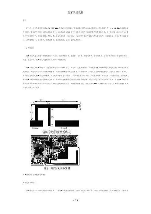
本文给出了一款倒F型天线的设计,该天线尺寸小,设计简约,制造成本低,工作效率高,适用于蓝牙系统应用。
1 天线设计倒F型天线是上世纪末发展起来的一种天线,具有结构简单、重量轻、可共形、制造成本低、辐射效率高、容易实现多频段工作等独特优点,因此,近几年来,倒F型天线得到了广泛的应用研究和发展。
倒F天线是在倒L天线abc的垂直元末端加上一个倒L结构edb构成。
它使用附加的edb结构来调整天线和馈电同轴线的匹配。
该天线具有低轮廓结构,辐射场具有水平和垂直两种极化,另外由于结构紧凑而且具有等方向辐射特性,同时其良好的接地设计可以有效提高天线的工作效率。
图1所示是典型的倒F型天线结构图,该天线可以看作是e端短路,a端开路的谐振器,所以,a端电压最大,电流为零,e端电压为零,电流最大。
由于倒F天线的结构中包含了接地的金属面,可以降低对射频模块中接地金属面的敏感度,因此非常适合用于片上系统。
另外,由于倒F天线只需利用金属导体配合适当的馈线来调整天线短路端到接地面的位置,因而制作成本较低,可以直接与PCB电路板焊接在一起。
图2所示为倒F型天线在电路板上的布置图。
倒F型天线在电路板上的布置图2 测量基本原理图3所示是一个网络分析仪的原理框图。
在对倒F天线进行测量时,先由仪器发出扫频信号,并将该信号通过输出口送到被测设备,当信号通过设备后,再送回网络分析仪。
网络分析仪的原理框图由于待测设备的输入阻抗与网络分析仪的输出阻抗不可能理想匹配,因而必然会发射一部分信号。
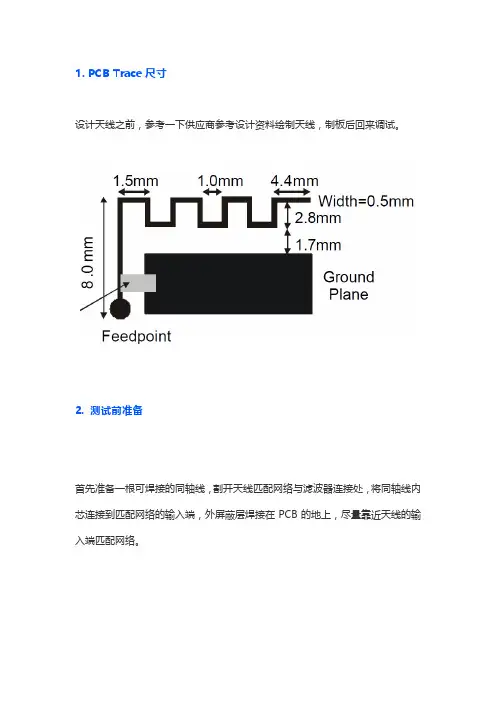
1. PCB Trace尺寸
设计天线之前,参考一下供应商参考设计资料绘制天线,制板后回来调试。
2. 测试前准备
首先准备一根可焊接的同轴线,割开天线匹配网络与滤波器连接处,将同轴线内芯连接到匹配网络的输入端,外屏蔽层焊接在PCB的地上,尽量靠近天线的输入端匹配网络。
3. VNA校准与调谐
VNA通过同轴电缆连接到产品上,可在同轴电缆外套上铁氧体磁环,铁氧体磁环有助于防止射频电流在同轴电缆外面流动(会干扰测量)。
对VNA Port1(单端口)使用电子校准件或者机械校准进行开路、短路、负载校准。
校准完毕后,将PCB和VNA连接,使用S11/Smith Chart测量输入端阻抗(注意调试时去嵌),可借助Smith Chart2.0 阻抗匹配软件调整匹配网络的LC电容电感的值来调谐,同时也可以切割Trace天线的长度,直到S11轨迹(显示在VNA)在中心频点2441MHz处的史密斯图,此时天线大致调谐完成。
4. 远场测试
使用VNA网络分析仪Smith Chart进行天线调谐后,还有必要进行微调,结合蓝牙产品的发射功能,从而使天线性能得到优化并最终定稿。
对于性能测试,最好是在半电波暗室中进行,能得到天线全部的指标。
但是往往现实不尽如人意,大多数工程师并不从事射频工作,从供应商直接采购蓝牙模组产品进行集成,对于天线更是一无所知。
因此,对于硬件工程师,我们可以使用简单的测试方法,在室内或室外距离产品2米处使用频谱仪接收功率(X,Y,Z三个方向进行评测),从频谱上的功率显示来判断天线性能。
测试过程中注意避免金属物体,如实验室金属桌、文件柜、灯柱和汽车等。
REVISED: 03.28.2018MSL = MSL-1RoHS/RoHS II Compliant3.2 x 1.6 x 1.2 mmPb FEATURESAPPLICATIONSItem Spec Frequency 2450MHz Bandwidth ≥90MHz Peak Gain 0.5 dBi typ.Average Gain -1 dBi typ VSWR <2:1Impedance 50 Ohm Power Capability3W max Operating Temperature Range-40ºC to + 85ºC • 2450MHz, bandwidth ≥90MHz• Small size - 3.2 x 1.6 x 1.2mm (0.125 x 0.62 x 0.047 inch)• Gain 0.5dBi (Peak) / -1dBi (Average)• VSWR <2:1• Non ground mounting type • Power handling 3W max • Matched to 50 Ohm• Suitable for RoHS compliant reflow • Wireless application - Bluetooth / WiFi (2.445GHz)• IoT devices• Bluetooth headsets or ear pieces • Industrial automation•Alternative to larger PCB solutionELECTRICAL CHARACTERISTICSAMCA31-101-2R450G-S1F-T3PackagingBlank: Bulk or Cut Tape T3 : T/R 3000pcs per reelPART IDENTIFICATIONREVISED: 03.28.2018MSL = MSL-1RoHS/RoHS II Compliant3.2 x 1.6 x 1.2 mmPb APPLICATION TEST CIRCUIT & PCB LAYOUTS – DEFAULT LAYOUTSEvaluation Board PCB LayoutShows the PCB layout highlighting the Ground and No Ground areas and trace feed line to the chip antenna.REVISED: 03.28.2018MSL = MSL-1RoHS/RoHS II Compliant3.2 x 1.6 x 1.2 mmPb MATCHING CIRCUIT AND REFERENCE VALUESChip antenna should be matched with the environment of final products. Normally this process can be done with capacitor or inductor.Range of Matching Component ValuesComponent DescriptionValue Antenna AMCA31-101-2R450G-S1F-T3----Capacitor *Series C 0.5 ~ 10 pF *Shunt C 33pF, 100 pF InductorSeries L 1.0 ~ 6nH Shunt L1.0 ~ 6nH*Series: Connected between antenna and feeding line in series. *Shunt: Connected between antenna and feeding line in parallelNote: Recommendation is to pre-place the π-type circuit layout circuit which will offer full flexibility to match the an -tenna to 50 Ohm in the final product layout with one of the match configurations below. Depending on matching, NC will apply to certain components.Range of Matching ConfigurationsNetwork AnalyzerElectrical Performance with matching circuit:Passive Test with Network AnalyzerREVISED: 03.28.2018MSL = MSL-1RoHS/RoHS II Compliant3.2 x 1.6 x 1.2 mmPb ANTENNA RESPONSE – SMITH CHART OF MATCH AND RETURN LOSS S11REVISED: 03.28.2018MSL = MSL-1RoHS/RoHS II Compliant3.2 x 1.6 x 1.2 mmPb OUTSIDE DIMENSIONS AND PCB LAND DRAWINGTERMINAL CONFIGURATIONTerminal identificationsTable (7.1) - Terminal ConfigurationNo Terminal Name NoTerminal NamePad 1Feed PointPad 2NCSeries A B C D E F G H I AMCA31 3.2±0.21.6±0.21.2±0.20.5±0.2 1.6±0.20.8±0.20.8±0.22.6±0.23.5±0.2This is the feed-line to the Antenna and should be matched to 50 Ohms based uponthe PCB dielectric parameters.(Dimensions in mm)REVISED: 03.28.2018MSL = MSL-1RoHS/RoHS II Compliant3.2 x 1.6 x 1.2 mmPb REFLOW PROFILE :• Preheat condition: 150 ~200 /60~120ºC sec. • Allowed time above 217ºC: 60~90sec. • Max temp: 260ºC• Max time at max temp: 10sec. • Solder paste: Sn/3.0Ag/0.5Cu • Allowed Reflow time: 2x max[Note: The reflow profile in the above table is only for qualification and is not meant to specify board assem -bly profiles. Actual board assembly profiles must be based on the customer’s specific board design, solder paste and process, and should not exceed the parameters as the Reflow profile shows.]REVISED: 03.28.2018MSL = MSL-1RoHS/RoHS II Compliant3.2 x 1.6 x 1.2 mmPb MANUAL SOLDERINGPre-heating Temperature: 120ºC, 60 ~ 300 sec.• Iron soldering power: Max.30W. • Pre-heating: 150 / 60 sec. ºC.• Soldering Tip temperature: 350 Max. ºC.• Soldering time: 3 sec Max. • Solder paste: Sn/3.0Ag/0.5Cu. • Max 1 times for iron soldering.• Soldering Temperature: 340ºC±5ºC, 5sec max per each terminal.[Note: Take care not to apply the tip of the soldering iron to the terminal electrodes.]PACKAGING: T3=3000 UNITS PER REELPackage Handling and Storage Precautions• The solderability of the external electrode may be deteriorated if packages are stored where they are exposed to high humidity. Package must be stored at 40 ºCor less and 70% RH or less.• The solderability of the external electrode may be deteriorated if packages are stored where they are exposed to dust of harmful gas (e.g. HCl, sulfurous gas of H2S).• Packaging material may be deformed if package are stored where they are exposed to heat of direct sunlight. • Solderability specified in Para 9.4 shall be guaranteed for 6 months from the date of delivery on condition that they are stored at the environment specified in Para 1.1. For those parts, which passed more than 6 months shall be checked solder-ability before use.REVISED: 03.28.2018MSL = MSL-1RoHS/RoHS II Compliant3.2 x 1.6 x 1.2 mmPb TAPE DIMENSIONS:REEL DIMENSIONS:W 8.0±0.10D0 1.50 +0.10 / -0.0P1 4.0±0.10P04.0±0.10E 1.75±0.10K01.50±0.10F 3.50±0.15A01.80±0.10B03.50±0.10t0.22±0.10Dimensions: mmDimensions: mmREVISED: 03.28.2018MSL =MSL-1RoHS/RoHS II Compliant3.2 x 1.6 x 1.2 mmPb CAUTIONSMounting Direction of Tape on ReelNote: The sprocket holes are to the right as the tape is pulled toward the user Ultrasonic cleaningUltrasonic vibration may cause deterioration & destruction of the component. Please avoid ultrasonic clean-ing.SolderingOnly leads of the component may be soldered. Please avoid soldering to any other part of the component, such as the Ag patterning as this will change the performance of the antenna.Handling & PackagingSee “Package Handling” for further details。
蓝牙倒F型天线的设计与测量蓝牙倒F型天线的设计与测量类别:通信网络0 引言蓝牙是一种支持设备短距离通信(一般是1Om之内)的无线电技术,能在设备之间进行无线信息交换,其工作频段是2.4~2.483 GHz的全球通信自由频段,目前已广泛应用在移动通信设备中。
天线是蓝牙无线系统中用来传送与接收电磁波能量的重要必备组件。
由于目前技术尚无法将天线整合至半导体芯片中,故在蓝牙模块里除了核心的系统芯片外,天线是另一个影响蓝牙模块传输特性的关键性组件。
本文给出了一款倒F型天线的设计,该天线尺寸小,设计简约,制造成本低,工作效率高,适用于蓝牙系统应用。
1 天线设计倒F型天线是上世纪末发展起来的一种天线,具有结构简单、重量轻、可共形、制造成本低、辐射效率高、容易实现多频段工作等独特优点,因此,近几年来,倒F型天线得到了广泛的应用研究和发展。
倒F天线是在倒L天线abc的垂直元末端加上一个倒L结构edb构成。
它使用附加的edb结构来调整天线和馈电同轴线的匹配。
该天线具有低轮廓结构,辐射场具有水平和垂直两种极化,另外由于结构紧凑而且具有等方向辐射特性,同时其良好的接地设计可以有效提高天线的工作效率。
图1所示是典型的倒F 型天线结构图,该天线可以看作是e端短路,a端开路的谐振器,所以,a端电压最大,电流为零,e端电压为零,电流最大。
由于倒F天线的结构中包含了接地的金属面,可以降低对射频模块中接地金属面的敏感度,因此非常适合用于片上系统。
另外,由于倒F天线只需利用金属导体配合适当的馈线来调整天线短路端到接地面的位置,因而制作成本较低,可以直接与PCB电路板焊接在一起。
图2所示为倒F型天线在电路板上的布置图。
2 测量基本原理图3所示是一个网络分析仪的原理框图。
在对倒F天线进行测量时,先由仪器发出扫频信号,并将该信号通过输出口送到被测设备,当信号通过设备后,再送回网络分析仪。
由于待测设备的输入阻抗与网络分析仪的输出阻抗不可能理想匹配,因而必然会发射一部分信号。
蓝牙模块的天线类别及特点
蓝牙模块天线是一种用来发射或者接收电磁波的元器件。
发射天线的作用主要是将发射机的高频电流能量有效地转换成空间的电磁能量;而接收天线的作用则恰恰相反,因此天线本质上可以说是一个能量转换器。
蓝牙模块常见的三种天线:陶瓷天线、PCB天线和IPEX外接天线来对比一下。
陶瓷天线是一种适合于蓝牙装置使用的小型化天线。
陶瓷天线又分为块状陶瓷天线和多层陶瓷天线。
块状天线是使用高温将整块陶瓷体一次烧结完成后再将天线的金属部分印在陶瓷块的表面上。
而多层天线烧制采用低温共烧的方式讲多层陶瓷迭压对位后再以高温烧结,所以天线的金属导体可以根据设计需要印在每一层陶瓷介质层上,如此一来可以有效缩小天线尺寸,并能达到隐藏天线目的。
由于陶瓷本身介电常数比pcb电路板的要高,所以使用陶瓷天线能有效缩小天线尺寸。
PCB天线是指无线接收和发射用的PCB上的部分。
发射时,它把发射机的高频电流转化为空间电磁波;接收时,它又把从空间截获的电磁波转换为高频电流送入接收机。
它的优点是:空间占用少,成本低,不需要单独组装天线,不易触碰损坏,整机组装方便,但有得必有失---牺牲性能。
缺点是:单个天线场型很难做到圆整,插损高,效率相对较低,容易受到主板上的干扰。
IPEX天线是一种作为射频电路和天线的接口,被广泛应用于无线局域网(WLAN)相关产品单板上。
它的优点是:场型能控制更好,插损低,信号的方向指向性好,效率高,抗干扰能力强,能远离主板上的干扰,而且不用过多的进行调试匹配,作为终端厂家,只需要外面接一个IPEX 的天线即可;
当然也有缺点:成本高,组装麻烦。